A Design Configuration of an FPGA-Based Coincident
Spectrometry System
Pham Dinh Khang1, Nguyen Nhi Dien2, Dang Lanh2, Nguyen Xuan Hai2, Pham Ngoc Tuan2, Nguyen Duc Hoa3, Nguyen An Son3
1Nuclear Training Center, Hanoi, Vietnam; 2Nuclear Research Institute, Dalat, Vietnam; 3University of Dalat, Dalat, Vietnam.
Email: [email protected]
Received July 8th, 2013; revised August 9th, 2013; accepted August 16th, 2013
Copyright © 2013 Pham Dinh Khang et al. This is an open access article distributed under the Creative Commons Attribution Li-cense, which permits unrestricted use, distribution, and reproduction in any medium, provided the original work is properly cited.
ABSTRACT
In the past, most of popular coincidence spectrometers were normally based on traditional electronics techniques such as time to amplitude conversion or logic selecting coincidence unit. They were complicated and it is not convenient for us to use them. This paper deals with a new design of a contemporary coincidence spectrometer which is based on Field Programmable Gate Arrays (FPGA) devices via Digital Signal Processing (DSP) techniques with Hardware Description Language (VHDL). The outstanding advantage of DSP techniques and FPGA technology is capable of enhancement of the quality of the experimental measurements for nuclear radiation. The designed configuration of the traditional system was tested on the PCI 7811R board of National Instruments while the digital systems were establishing with FPGA de-vices. The purpose of this work is referring to the principle for construction of an FPGA-based system capable of re-placing a conventional system. Therefore, a novel approach for in-house development of digital techniques is presented. The method for designing the system is utilization of slow-fast coincidence configurations with two HPGe detectors obtaining a pair of coincidence events, processing data in DSP algorithms. The significant and noticeable results are the operating frequency of 80 MHz and system timestamp window of approximately 10 ns.
Keywords: Digital Signal Processing; FPGA; VHDL
1. Introduction
A spectrometry system is used to measure nuclear radia- tion including X-rays, gamma rays, alpha and beta rays, neutrons and other heavy charged particles. Most of these applications require the identification of radiation sour- ces and relative concentration of each source. The ex-perimental measurements in nuclear physics may include counting events, getting information about energy-timing, and their combinations. Typically, these main parameters are changed in the measurement of radiation energy range and speed of the whole event. Decay scheme and lifetime studies, coincidence experiments, single-photon counting, and position annihilation studies are some of the experimental areas that require good timing capabili- ties [1]. As well-known, all of the traditional spectrome- try systems were not much convenient because of com- bining properly functional electronics modules in the Nuclear Instrumentation Modules (NIM) or the Com- puter Automated Measurement and Control (CAMAC) standards [2,3]. In the two-past decades, at Nuclear Re-
electronics modules as well as the economic investment [7,8]. Besides, an important element of the system based on DSP and FPGA is low power consumption to save energy that has a special meaning in large equipments. With these advantages, the applied research via FPGA, DSP in design and fabrication of radiation measurement instruments for fundamental research in nuclear physics, especially about the study of nuclear structure and data on neutron beams at the Dalat reactor and on the charged particle beam accelerators for domestic needs is essential.
2. The Basis and Method for the Design
2.1. The Basis for Operation of an
“Event-Event” Recording Coincidence Spectrometer Using TAC
An “event-event” recording coincidence spectrometer for processing data under a combination of the traditional analog electronics and interfacing unit is shown in Fig- ure 1. The standalone spectrometer is capable of linking to PC through a Peripheral Component Interconnect (PCI) slot. The system consists of two channels: the upper channel and the lower one. All of the functional elec- tronics modules are as follows:
Spectroscopy amplifier (AMP), model 572A, Can- berra;
Fast peak sensing Analog to Digital Converter-(ADC) 8 k, model 7072, FAST CompTec;
High Voltage (HV) bias supply, model 660, Ortec; Timing Filter Amplifier (TFA), model 474, Ortec; Constant Fraction Discriminator (CFD), model 584,
Ortec;
Delay unit, model 2058, Canberra;
Time to Amplitude Converter (TAC), model 566, Ortec;
Peak sensing ADC 16 k, model 8713, Canberra. The principal operation of the system is as follows (refer to Figure 1): The signals appearing on the energy (E) outputs from two HPGe detectors are fed to both the inputs of two AMPs belonging to the upper and lower channels. In addition, two timing (T) outputs are also coming to the inputs of two TFAs. Next, the two-TFA outputs are fed to the inputs of CFDs. The upper CFD output will then strobe the “Start” input TAC, and the other CFD output plays a role of stopping the TAC in one converting cycle for changing signal amplitude. When the interfacing unit 7811R receives “Valid conver- sion” signal from TAC, it will soon send back three “Gate” signals for gating all of ADCs; and at that time, ADCs are allowed to convert amplitude into BCD code numbers. After ADCs finish conversion cycles, the in- terfacing unit will read the code and write these values into memory.
After finishing write operation, ADCs return to an idle status and wait for another gate signal under the control of the next valid conversion signal. ADCs have no opera- tion if there is no strobe signal at the gate regardless of incoming signals at their inputs. In a data file, the data will be arranged into three columns E1(n), E2(n) and
E3(n). The values of E1(n) and E2(n) are in turn the am-
plitude code numbers of the two coincidence pulses coming from detector 1 and detector 2 respectively, E3(n)
[image:2.595.121.475.491.721.2]is a value corresponding to the differential time between two events, n is the ordinal number of pairs of coinci- dence events from the beginning of measurement. After finishing the measurement, data is handled by the multi-
variable statistics processing program to obtain informa- tion about energy, transition intensity and decay scheme of nuclei on research. Dead time (DT) of the system will be calculated as the shortest interval between two pairs of consecutive amplitude codes recorded via spectrometer. Total DT of the system depends on the sampling rate of ADC and data-transfer speed of interfacing unit. The slower they work, the longer dead time, and vice versa. Because DT is one of the causes affecting the system’s efficiency, therefore it should be ensured that the shorter the DT, the higher the data.
min 1 2 3 4
where τ1: delay of spectroscopy amplifier, τ2: shaping
time, τ3: ADC’s conversion time, and τ4: time for data
transfer operation of the interfacing unit.
2.2. The Principle for Design of an “Event-Event” Recording Digital Coincidence Spectrometer
Figure 2 shows the block diagram of an “event-event” recording digital coincidence spectrometer. Its operation principle is as follows: when the radiation signals are recorded from detector 1 or detector 2, DSPs analyze the amplitude of the pulses and then give the corresponding values of (A1, A2). At the same time, when the signals
exceed the lower thresholds, DSPs will read more the values corresponding to the moments of (t1, t2) at those
the pulses exceed the aforementioned thresholds. The timing tester will determine the time difference between
the two events Δt = |t1 – t2|. If ΔW is called coincidence
time window of the system, there are a number of cases occurred as follows:
Δt ≤ΔW: coincidence occurred. The programmer will write pair of events into memory with contents of A1, A2
and Δt.
Δt > ΔW: non-coincidence occurs. The program will remove pair of events.
In the second case, assuming that there was an event appeared beforehand on the first channel, the program will remove the values of A1 and Δt out of temporary
memories and wait for the next event occurring on it. Value of t1 will be compared to that of t2 so as to deter-
mine the next pair of coincidence events. Thus, the proc- ess keeps on until the measurement finishes.
3. Analysis and Assessment of the Design
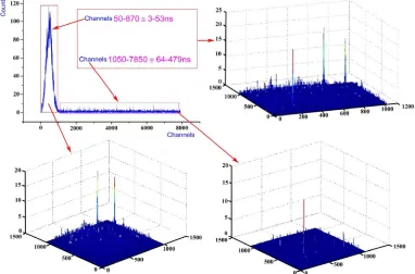
[image:3.595.334.515.355.420.2] [image:3.595.107.489.466.718.2]As physical side, test results for the block diagram in Figure 1 are presented in Figure 3. The test measure- ment was carried out with 60Co, activity ~20 kBq and 137Cs, activity ~100 kBq, measurement range of TAC
Figure 2. The block diagram of an “event by event” re- cording digital coincidence spectrometer.
was 500 ns. The obtained results showed that on the basis of the time difference of pairs of coincidence events be- tween the two detectors, the spectra corresponding to
60Co and 137Cs could properly be separated with high
precision. Drawback of the configuration was that the performance of the system reduced because of fixed time interval during the inputs of Start and Stop of TAC; therefore, a modification of circuit design which can re- place the role of traditional start and stop signals had to be established. The modified circuit is called time-stamp one. In the second configuration, the flexibility of vary- ing timestamp at which a triggering event occurred will allow us to overcome the aforementioned drawback. For the semiconductor detector when the incoming radiation interacts with the positions at the edge of crystal, the charge collecting time will tend increasing. This leads the rising edges of the pulses at the preamplifier’s outputs pulled longer. If the operation frequency of the signal processing circuit is not high enough, or algorithm for determination of threshold-crossing time is not so good (due to jitter or walk), the timing resolution of the system will become worse significantly. If the frequency of the circuit is called f0, error for determining time stamp will
be ±1/f0 (sec). For instance, if f0 is equal to 40 MHz, the
time error will be ±25 ns. To test this, PCI interfacing unit has been programmed for running at 80 MHz, the signals at the inputs (Start, Stop) of TAC were postponed with a number of different time intervals owning to nanosecond-delay module, Canberra. The final results showed that error in determining the threshold crossing time is 12.5 ns.
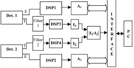
To overcome the above-mentioned restrictions as us- ing HPGe detectors, it is better to add an algorithm capa- ble of removing the pulses that have the slow rising edges into DSPs. However, the additional algorithms can make processing speed to become slow, especially for determining the height of peak. Therefore, in this case the third configuration should be used in order to over- come this drawback (see Figure 4). This design allows separating and processing properly timing signals. As a result, the pulses having the slow rising edges are re-
Figure 4. The principal design of digital “event-event” coin-cidence system with addition of filtering time circuit.
moved via filtering circuits before coming to the digital processing parts will play a role in determining the threshold crossing time. In the case of having no coinci- dence signal, data reading algorithms have to be modi- fied in order to remove amplitude value A1 or A2 because
the filtering circuit rejected almost of the non-suitable pulses.
4. Conclusions
This work presents the two-different radiation measure- ment systems for detecting pairs of coincidence events. They are the traditional coincidence spectrometer and the DSP-based one, respectively. Obvious drawback of the first system is cumbersome in size, adjusting operation and synchronizing signals among electronics stages. On the contrary, both of the two digital systems can over- come the above-mentioned drawback owing to the flexi- bility of varying time-stamp window, and of the con- figurations inside FPGA entities. In addition, the design of system based on DSP techniques using FPGA allows constructing a compact and impact coincidence spec- trometer in which all of parameters are selected and con- trolled by the application software. In the reality, DSP algorithms are completely digitized by the Very high speed integrated circuit VHDL, therefore, the digital system is truly faster than the traditional system.
The significance and the importance of this work are that it contributes partly into the application and devel- opment of some radiation measurement systems based on DSP techniques using FPGA. So far, the diagrams in both of Figures 2 and 4 have been studying and fabric- cating at the Department of Nuclear Physics and Elec- tronics, NRI, Dalat. From the point of nuclear electronics instruments, the design of system ought to be the basis for development and application of coincidence meas- urement techniques in the field of physics research and radiation detection. Moreover, in the case of modifying the structure of its hardware, it can also be used in con- struction of a part of a Compton suppression spectrome- try system—one of the most important gamma-ray spec- trometers applied in experimental nuclear physics.
REFERENCES
[1] EG&G ORTEC Catalog, “Nuclear Instruments and Systems Catalogue,” 1987.
[2] A. M. Hoogenboom, “A New Method in Gamma-Ray Spectroscopy: A Two Crystal Scintillation Spectrometer with Improved Resolution,” Nuclear Instruments, Vol. 3, No. 2, 1958, pp. 57-68.
doi:10.1016/0369-643X(58)90092-6
[image:4.595.59.288.593.710.2]Gamma Coincidence Spectrometer for Research on Nu- clear Structure at DNRI,” Proceedings of International Symposium on Instrumentation of Small and Medium Ac-celerators, Tsukuba, 1996, pp. 128-131.
[5] P. D. Khang, N. X. Hai, V. H. Tan and N. N. Dien, “Ga- mma-Gamma Coincidence Spectrometer Setup for Neu- tron Activation Analysis and Nuclear Structure Studies,” Nuclear Instruments and Methods in Physics Research, Vol. 634, No. 1, 2011, pp. 47-51.
[6] A. Kimura, Y. Toh, et al., “Development of a Data Ac- quisition System for a Multiple Gamma-Ray Detection Method,” AIP Conference Proceedings, Vol. 769, Mel-
ville, New York, 2005.
[7] M. J. Koskelo, I. J. Koskelo and B. Sielaff, “Comparison of Analog and Digital Signal Processing Systems Using Pulse,” Nuclear Instruments and Methods in Physics Re-search, Vol. 422, No. 1-3, 1999, pp. 373-378.
![Figure 1. The block diagram of TAC-based coincidence spectrometer used at NRI [5].](https://thumb-us.123doks.com/thumbv2/123dok_us/7855896.736268/2.595.121.475.491.721/figure-block-diagram-tac-based-coincidence-spectrometer-used.webp)