http://www.scirp.org/journal/cs ISSN Online: 2153-1293
ISSN Print: 2153-1285
Data Intelligent Low Power High Performance
TCAM for IP-Address Lookup Table
K. Mathan
1, T. Ravichandran
21Department of Electrical and Electronics Engineering, Hindusthan College of Engineering and Technology, Coimbatore, India 2Dean and HoD, SNS College of Tecnology, Coimbatore, India
Abstract
This paper represents current research in low-power Very Large Scale Integration (VLSI) domain. Nowadays low power has become more sought research topic in electronic industry. Power dissipation is the most important area while designing the VLSI chip. Today almost all of the high speed switching devices include the Ternary Content Addressable Memory (TCAM) as one of the most important features. When a device consumes less power that becomes reliable and it would work with more ef-ficiency. Complementary Metal Oxide Semiconductor (CMOS) technology is best known for low power consumption devices. This paper aims at designing a router application device which consumes less power and works more efficiently. Various strategies, methodologies and power management techniques for low power circuits and systems are discussed in this research. From this research the challenges could be developed that might be met while designing low power high performance circuit. This work aims at developing Data Aware AND-type match line architecture for TCAM. A TCAM macro of 256 × 128 was designed using Cadence Advanced Devel-opment Environment (ADE) with 90 nm technology file from Taiwan Semiconduc-tor Manufacturing Company (TSMC). The result shows that the proposed Data Aware architecture provides around 35% speed and 45% power improvement over existing architecture.
Keywords
Low Power, TCAM, Switching Power, Match Line, Searchline, Data Aware and Speech Processing
1. Introduction
Power consumption is a major problem while designing VLSI circuit. Few technologies How to cite this paper: Mathan, K. and
Ravichandran, T. (2016) Data Intelligent Low Power High Performance TCAM for IP-Address Lookup Table. Circuits and Sys- tems, 7, 3734-3745.
http://dx.doi.org/10.4236/cs.2016.711313
Received: March 31, 2016 Accepted: April 15, 2016 Published: September 16, 2016
Copyright © 2016 by authors and Scientific Research Publishing Inc. This work is licensed under the Creative Commons Attribution International License (CC BY 4.0).
http://creativecommons.org/licenses/by/4.0/
were adapted to reduce the power consumption while designing VLSI circuit. One of the technologies is CMOS. Network routers which are used for the packet data trans-mission, go through the process of IP address matching technique. The matching tech-nique requires the lookup table which has the problem of multiple data access. The new idea of content addressable memory (CAM) is the most popular hardware solution to support the high lookup table speed. The CAM is address by data rather than by ad-dress. Since search can be done in parallel, it leads to faster data search than the soft-ware lookup. The CAM is widely used in Translation Look aside Buffer (TLB), high as-sociative cache, image processing, database and network routers, etc.; all require fast ta-ble lookup.
The routers used in the network applications demand a high speed TCAMs for pack-et filtering. The TCAM provides the fast look-up table for data and address routing. The network router uses the TCAM and SRAM cell which is used to provide the high speed searching and data storage capacity. However on the fabricating side of TCAM it occupies a large silicon area space. It also creates the problem of stability. Since it occu-pies a huge area comparatively the power consumption of the TCAM increases drasti-cally. There is a huge power-dissipation problem because of the search operation which is carried out parallel in a chip which is of large size. Just because of the large power dissipation the reliability of the chip is questioned and this again leads to the problem of increase in the package cost of the IC. There were many works reported on the at-tempt of reducing the power dissipation but that failed to solve the problem of area overhead and noise immunity. Another important problem is the reduction in the yield.
Because of these problems, it attributes to the following shortcomings: 1) increase in chip size, 2) increase in power dissipation, and 3) reduction in the yield, which lead to a production cost overhead. They have to be solved to realize cost-efficient large-scale TCAM chips.
For power consumption, a TCAM consumes power mainly in 3 parts: clock and con-trol, match line, and search line (SL). Thanks to the advancement of match-line design techniques, the power consumption of the former has been greatly reduced. This can be seen from the works of the past three years [1]-[3], where the power consumption for search lines occupies about 54%, 71%, and 82% of the total power, respectively. To tackle the power consumption problem on search lines, pipelining and hierarchical search lines are used in [4]. However, the area and power overhead caused by the pipe-line flip-flops and the clock driver diminish the usefulness of the approach.
In contrast, this paper introduces a low-power TCAM design that consists of two newly developed schemes, i.e., the refined search enable (RSE) and “don’t care” gating (DCG) schemes. Without any performance penalty and complex control circuitry, our design can largely reduce the TCAM power dissipated in the SLs by minimizing both the SL switching activity and the average power consumption per SL switch.
In this paper, we propose a novel Data Aware TCAM (DATCAM) cell which consists of improved Search Enable Line (SEL) and Data Aware Intelligent “Don’t Care” Gating (DAIDCG) to solve the problems of power consumptions. The proposed architectures are attractive for realizing small chip size, low-power and high-throughput operation. In addition the architecture has a great impact on the yield improvement. A 4.5-Mb DATCAM design verifies these advances quantitatively.
2. Proposed Designs
2.1. Proposed Data Aware TCAM (DATCAM)
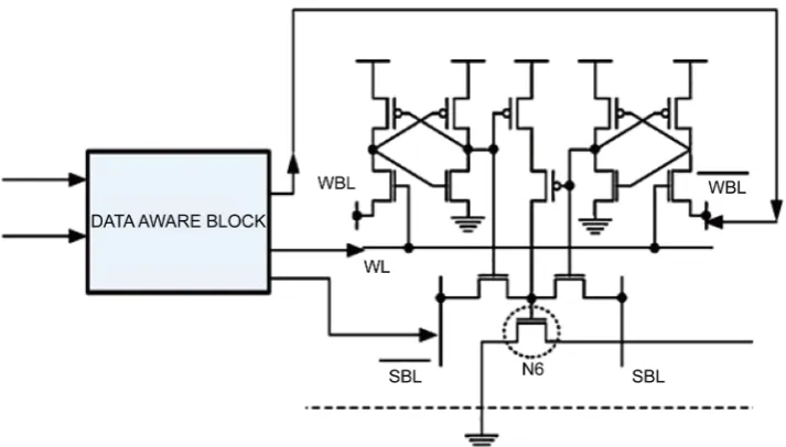
Data aware proposed TCAM cell is shown in Figure 1, which consists of a data aware block to reduce the redundant computation word bit line WBL and its complement address select line SBL and a discharge transistor N6 [12] [13].
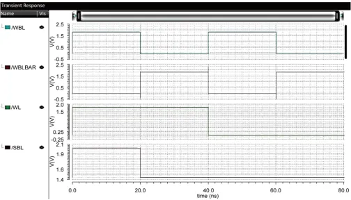
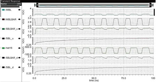
[image:3.595.194.551.479.682.2]The back to back connected inverted store the value. The simulated lines for different signal are shown in Figure 2. Figure 3 shows the simulated results of the write opera-tion in the TCAM cell. The signal in Figure 2 shows the write bit line (WBL) and its complement (WBLBAR), word line (WL) and select Bit line (SBL). The timing diagram show the storing/write operation being performed for every word line with the select bit line giving the signal for selection.
Figure 3 shows the signals write bit line (WBL), its complement (WBLBAR), word line (WL) and Select Bit line (SBL). The timing diagram show the write “1” operation being carried out in the DATCAM cells.
Figure 2. Simulated output of the TCAM cell.
[image:4.595.46.551.403.691.2]2.2. Gating Nodes (GN) Module Design
In order to gate the search data from being broadcast over the entire SL, our design in-serts the GNs to break the entire SL into several segments. As shown in Figure 4, the GN can be easily implemented as a controllable inverter whose function is enabled/ disabled by the corresponding mask bit. For example, if the GN is located on the ih cell, the mask value of the ih cell M
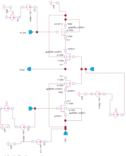
i will determine whether the search data can be propa-gated forward or not. When the th cell is in “X” state, it will cut off both the power and ground sources to deactivate the inverter to further transmit the search data. Otherwise, the inverter will take effect in case of Mi = 0. i.e., “0” or “1” state. The number of cells between two Gns is the definition ot the granularity (G) of DCG scheme. It is critical to optimize both search performance and power saving. If G is too large, the probability that the first cell of segment is “X” is low, such that the amount of effective capacitance reduction is insignificant. In contrast, small GN can largely reduce the effective capa-citance, but its defect point is the serious propagation delay. In this case, since the number of GNs is too large, the large total inverter delay is detrimental to the data propagation from the first segment to the last segment, such that the degradation in search performance is inevitable. Therefore, an adequate G that benefits both power saving and search performance is very critical to our design. The detailed analysis will be provided in the experimental results. Figure 5 shows the simulated results of the GN module. In Figure 5 the gating operation is done in the read/write operation for the CAM cell the time period of the gating operation is decided by the critical path timing of the DATCAM cell designed which is around 5 ps. The transient response shows the timing diagram of the write operation which is being gate by a clock select signal s and its complement s’.
2.3. Data Aware Intelligent Don’t Care Gating (DAIDCG)
Figure 5. Simulated results of GN output.
Table 1. Search data example of five consecutive 0. Case A/B is the TCAM design without/with SE scheme.
Search Data Case A: Without SC Case B: With SC
S S Bar S S Bar
0 0 1 0 1
0 0
0 0 1 0 1
0 0
0 0 1 0 1
0 0
0 0 1 0 1
0 0
0 0 1 0 1
N0→1 = 4 N0→1 = 0
SE scheme can be observed from the case B shown in the Table 1. Compared to the conventional TCAM without ISEL scheme [16], the unnecessary transitions are all eliminated.
[image:8.595.192.553.434.684.2]In the traditional TCAM if the cell is matched in the evaluation phase, then the pull-down path is conducted, whose length is three transistors, i.e., N1, N2, and N3. The number of transistor in the critical path is high for A in the worst case, in which only one TCAM cell is matched, the increased path would lengthen the time to dis-charge the ML to 0. Thus, the search performance degradation is inevitable. In order to eliminate the aforementioned performance penalty, the pull-down logic of TCAM cell is refined, as illustrated in Figure 7. During the evaluation phase, i.e., N3 is conducting, there are two possible cases. 1) If the TCAM0 cell is in “X” state, N4 controlled by M is turned off to block the transmission of the XOR result. At the same time, M = 1 will conduct N2 to discharge node Z. Thus, N1 is turned off to disconnect the pull-down path, such that the ML is still high. This is a wild match. 2) In the other case, M = 0 will
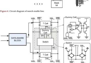
Figure 6. Circuit diagram of search enable line.
result in such that N2 is OFF, and N4 is ON. Thus, node Z follows the XOR result to control N1. The ML is discharged to 0 only when S is not equal to D. Since the length of the conducted pull-down path (P1) is 2, the proposed design can achieve the same search performances the conventional TCAM design without the SE scheme. Figure 8 shows the segmented cell simulated output results [17].
2.4. Segmented Cell Architecture
In Figure 7 the cells marked as “x” is used to represent the mask (don’t care) bits and the example in IP ADDRESS lookup in a progressive pattern. This is used to save the energy because these x cells need not be used with the search line. But can be used just to pass the signals [18].This becomes the foundation for the segmented search line de-sign as shown in Figure 7. Energy is saved by writing a “x” in the upper T cell. While doing so the bit and the bit bar are raised high [19]. Out put of the dummy cell q be-comes low so that the search path would be cut off and the upper segment of the search line pulled to ground. This inturn would save the energy.
3. Analysis and Observations
[image:9.595.45.552.419.685.2]The circuits are designed with an intention of making the circuit intelligent enough to detect the computation based on the signal correlation and also it tries to reduce the unnecessary switching in the circuits. This subsequently reduces the power consump-tion of the circuits. The circuits are constructed using virtuoso of cadence and simu-lated using the spectre. The circuits were simusimu-lated using the model file of 90 nm from
Table 2. Comparison of the proposed design with the existing works.
Work Technology (nm) Voltage (v) Search time (ns) Energy (fJ)/search/bit
Jinn Shyan et al. 130 1.2 1.10 0.35
Igor Arsovski et al. 130 1.2 1.40 2
Conventional 180 1.8 3.04 3.7
This work 90 1 0.82 0.16
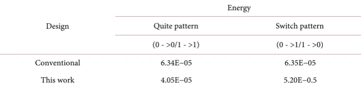
Table 3. Energy comparisons with input pattern.
Design
Energy
Quite pattern Switch pattern
(0 - >0/1 - >1) (0 - >1/1 - >0)
Conventional 6.34E−05 6.35E−05
This work 4.05E−05 5.20E−0.5
TSMC library. The Verilog simulated in the Modelsim is used in the digital porion of the study design. The results are compared with the previous work in this domain. Ta-ble 2 and TaTa-ble 3 show the comparison of the simulated results.
For accurate evaluation, we use the TSMC 0.18-CMOS technology to layout three IPv4 routing tables, and all data are obtained from the post layout simulation. The table size is fixed at 128 * 32, i.e., 128 entries by 32 bits, for all tables.
4. Conclusion
This paper tries to develop a data aware AND-type match line architecture and com-plexity less improved search line architecture for TCAM. The proposed architecture in search line tries to explore the feasibility of power reduction in the search line by ex-ploiting the inter- and intra-data dependencies. A TCAM Marco of 256 × 128 b was de-signed using Cadence ADE with 90 nm technology file from TSMC. The simulated re-sults show that the proposed data aware architecture provides around 40% reduction in search time and 55% reduction in the energy consumption over the existing architec-ture.
References
[1] Arsovski, I., Chandler, T. and Sheikholeslami, A. (2003) A Ternary Content Addressable Memory (TCAM) Based on 4T Static Storage and including a Current-Race Sensing Scheme. IEEE Journal of Solid-State Circuits, 38, 155-158.
http://dx.doi.org/10.1109/JSSC.2002.806264
[2] Arsovski, I. and Sheikholeslami, A. (2003) A Mismatch-Dependent Power Allocation Tech-nique for Match-Line Sensing in Content-Addressable Memories. IEEE Journal of Solid- State Circuits, 38, 1958-1966. http://dx.doi.org/10.1109/JSSC.2003.818139
[image:10.595.193.551.209.295.2]Integrated Circuits Conference, September 2003, 383-386.
http://dx.doi.org/10.1109/cicc.2003.1249423
[4] Choi, S., Sohn, K., Lee, M.-W., Kim, S., Choi, H.-M., Kim, D., Cho, U.-R., Byun, H.-G., Shin, Y.-S. and Yoo, H.-J. (2004) A 0.7 fJ/Bit/Search, 2.2 ns Search-Time, Hybrid Type TCAM Architecture. IEEE International Solid-State Circuits Conference Digest of Technic-al Papers, February 2004, 498-499.
[5] Noda, H., Inoue, K., Kuroiwa, M., Igaue, F., Yamamoto, K. and Mattausch, H. (2005) A Cost-Efficient High-Performance Dynamic TCAM with Pipelined Hierarchical Searching and Shift Redundancy Architecture. IEEE Journal of Solid-State Circuits, 40, 245-253.
http://dx.doi.org/10.1109/JSSC.2004.838016
[6] Agrawal, B. and Sherwood, T. (2008) Ternary CAM Power and Delay Model: Extensions and Uses. IEEE Transactions on Very Large Scale Integration (VLSI) Systems, 16, 554-564.
http://dx.doi.org/10.1109/TVLSI.2008.917538
[7] Wang, J.S., Wang, C.C. and Yeh, C. (2006) TCAM for IP-Address Lookup Using Tree-Style AND-Type Match Lines and Segmented Search Lines. International Solid State Circuits Conference, 577-586.
[8] Huang, P.T., Chang, S.W., Liu, W.Y. and Hwang, W. (2007) A 256 × 128 Energy-Efficient TCAM with Novel Low Power Schemes. Proceedings of the International Symposium on VSLI Design, Automation and Test (VLSI-DAT), 1-4.
http://dx.doi.org/10.1109/vdat.2007.373204
[9] Yang, B.D. and Kim, L.S. (2005) A Low-Power CAM Using Pulsed NAND-NOR Match- Line and Charge-Recycling SL Driver. IEEE Journal of Solid-State Circuits, 40, 1736-1744.
http://dx.doi.org/10.1109/JSSC.2005.852028
[10] Wang, J.-S., et al. (2005) An AND-Type Match-Line Scheme for Energy-Efficient Content Addressable Memories. ISSCC Digest of Technical Papers, February 2005, 464-467.
[11] Arsovski, I., et al. (2003) A Current-Saving Match-Line Sensing Scheme for Content- Addressable Memories. ISSCC Digest of Technical Papers, February 2003, 304-305.
http://dx.doi.org/10.1109/isscc.2003.1234309
[12] Noda, H., Inoue, K., Kuroiwa, M., Amo, A., Hachisuka, A., Mattausch, H.J., Koide, K., Soe-da, S., Dosaka, K. and Arimoto, K. (2004) A 143 MHz, 1.1 W, 4.5 Mb Dynamic TCAM with Hierarchical Searching and Shift Redundancy Architecture. IEEE International Solid-State Circuits Conference Digest of Technical Papers, February 2004, 208-209.
[13] Yamagata, T., Mihara, M., Hamamoto, T., Murai, Y., Kobayashi, T., Yamada, M. and Ozaki, H. (1992) A 288-kb Fully Parallel Content Addressable Memory Using a Stacked-Capacitor Cell Structure. IEEE Journal of Solid-State Circuits, 27, 1927-1933.
http://dx.doi.org/10.1109/4.173123
[14] Choi, S., et al. (2004) A 0.7 fJ/Bit/Search, 2.2 ns Search Time, Hybrid Type TCAM Archi-tecture. ISSCC Digest of Technical Papers, February 2004, 498-507.
[15] National Chung Hsing University, Taichung [Online]. http://www.nchu.edu.tw
[16] Shah, D. and Gupta, P. (2001) Fast Updating Algorithms for TCAMs. IEEE Micro, 21, 36- 47. http://dx.doi.org/10.1109/40.903060
[17] Lin, C.S., Chang, J.C. and Liu, B.D. (2003) A Low-Power Precomputation-Based Fully Pa-rallel Content Addressable Memory. IEEE Journal of Solid-State Circuits, 38, 654-662.
http://dx.doi.org/10.1109/JSSC.2003.809515
http://dx.doi.org/10.1109/TVLSI.2006.871760
[19] Baeg, S. (2008) Low Power Ternary Content-Addressable Memory Design Using a Seg-mented Match Line. IEEE Transactions on Circuits and Systems I: Regular Papers, 55, 1485-1494. http://dx.doi.org/10.1109/TCSI.2008.916624
Submit or recommend next manuscript to SCIRP and we will provide best service for you:
Accepting pre-submission inquiries through Email, Facebook, LinkedIn, Twitter, etc. A wide selection of journals (inclusive of 9 subjects, more than 200 journals)
Providing 24-hour high-quality service User-friendly online submission system Fair and swift peer-review system
Efficient typesetting and proofreading procedure
Display of the result of downloads and visits, as well as the number of cited articles Maximum dissemination of your research work