DEVICE DESIGN, AND TESTING
by
Mahesh Satyanarayana Ailavajhala
A dissertation
submitted in partial fulfillment of the requirements for the degree of
Doctor of Philosophy in Electrical and Computer Engineering Boise State University
© 2014
DEFENSE COMMITTEE AND FINAL READING APPROVALS
of the dissertation submitted by
Mahesh Satyanarayana Ailavajhala
Dissertation Title: Nano-Ionic Radiation Sensor: Materials Engineering, Device Design, and Testing
Date of Final Oral Examination: 13 March 2014
The following individuals read and discussed the dissertation submitted by student Mahesh Satyanarayana Ailavajhala, and they evaluated his presentation and response to questions during the final oral examination. They found that the student passed the final oral examination.
Maria I. Mitkova, Ph.D. Chair, Supervisory Committee
Darryl Butt, Ph.D. Member, Supervisory Committee
Dmitri Tenne, Ph.D. Member, Supervisory Committee Vishal Saxena, Ph.D. Member, Supervisory Committee Carlo G. Pantano, Ph.D. External Examiner
iv DEDICATION
To My Parents and
v
ACKNOWLEDGEMENTS
I would like to thank my advisor, Dr. Maria Mitkova, for her guidance, patience, and continued encouragement throughout my time at Boise State University.
Dr. Mitkova’s guidance was vital for my understanding of chalcogenide glasses, and amorphous material. The conversations with her always included fruitful advice about research, and life, and it is a great pleasure to be her student during my tenure.
vi
This research has been made possible with financial support from: Boise State University Department of Electrical and Computer Engineering, Department of Energy – Nuclear Engineering in University Program (DOE-NEUP), NASA EPSCOR, and
vii ABSTRACT
For decades, various radiation-detecting materials have been extensively researched, to find a better material or mechanism. Recently, there has been a growing need for smaller, and more effective materials or devices that are Integrated Circuits (IC) compatible, and can perform similar functions as bulkier Geiger counters, and other measurement options, which fail the requirement for easy, cheap, and accurate radiation dose measurements. Here arises the use of thin films of chalcogenide glasses, which have unique properties of high thermal stability along with high sensitivity towards short wavelength radiation.
In this work, the effect of γ-rays, generated from a 60Co source, on the properties of thin films chalcogenide glasses was studied. Various film compositions from different germanium containing chalcogenide glass systems, i.e., Ge-S, Ge-Se, and Ge-Te, were investigated. These materials are the most thermally stable among the chalcogenide glasses, therefore they were studied to get a broad perspective of the development of structures, and the effect of chemical bonding under different radiation doses.
viii
within the specific films. Additionally, X-ray Photoelectron spectroscopy (XPS), and Atomic Force Microscopy (AFM) provided insight into the topological transformation associated with the underlying structural changes. Along with the bare films, radiation-induced silver diffusion was studied to understand the role, and effect of silver during a radiation event. The introduction of silver creates different silver containing products that aid or hinder the increase in the film conductivity. These silver containing films were investigated using X-ray diffraction, and elemental mapping to determine the silver containing products, crystal sizes, rate of silver diffusion, and the oxidation rate due to radiation dose. These results were discussed based on the particular structures of the glasses, and the existing models. This information was also used as inputs in order to model, and simulate the real time diffusion of silver using COMSOL multiphysics
software. Combined, these results provided a partial view of the mechanisms contributing to the device performance.
After careful considerations of the various effects on the conductivity of the films, several device designs were fabricated, and their electrical performances are presented as a function of radiation dose. Three distinct generations of devices were created, each of which has offered a different methodology for amplifying the effects determined in the film analysis. Two generations of devices (Gen. 1, and Gen. 2) were fabricated using a laterally diffusing silver source while Gen. 3 devices were created with a specific
ix
x
TABLE OF CONTENTS
DEDICATION ... iv
ACKNOWLEDGEMENTS ... v
ABSTRACT ... vii
LIST OF TABLES ... xiv
LIST OF FIGURES ... xvi
LIST OF ABBREVIATIONS ... xxvii
INTERACTION OF MATTER WITH LIGHT ... 1
Wave Particle Duality ... 1
Radiation ... 2
The Origin of γ-rays ... 4
Characteristic of Nuclear Decay ... 5
Sources of Gamma Radiation ... 6
Gamma Ray Interaction with Matter ... 7
Compton Effect ... 10
Photoelectric Effect ... 13
Pair Production... 14
TYPES OF DETECTORS ... 16
Gas-Filled Detectors ... 16
xi
Semiconductor Detectors ... 19
Ge Crystals ... 20
Cadmium Zinc Telluride (CZT)... 22
CHALCOGENIDE GLASSES, AND RADIATION-INDUCED EFFECTS ... 27
Basics of Glasses... 27
Sub-Bandgap Light ... 35
Structural Changes ... 35
Optical Properties ... 39
Gamma Radiation ... 44
Structural Changes ... 44
Optical Properties ... 50
Chalcogenide Glasses as Dosimeters ... 52
Silver Containing Chalcogenide Glasses ... 57
Silver Diffusion Properties ... 57
Cluster Bypass Model ... 62
Diffusion Products ... 64
Germanium Containing Glasses ... 70
FILM CHARACTERIZATION METHODS ... 75
Methods of FILM ANALYSIS ... 75
Spectrophotometer ... 75
X-ray Photoelectron Spectroscopy (XPS) ... 76
Energy Dispersive X-ray Spectroscopy (EDS) ... 76
xii
FILM ANALYSIS ... 83
Film Fabrication ... 83
Bare Films ... 83
Silver Covered Films ... 86
Results, and Discussion ... 89
Bare Film Results ... 89
Discussion ... 104
Silver-Containing Film Results... 113
Discussion ... 119
Silver Diffusion Simulations... 122
Conclusion ... 131
GENERATION 1 DEVICES ... 133
Device Fabrication ... 133
UV Characterization ... 137
Gamma Ray Characterization ... 139
Ge-S Based Devices ... 139
Ge-Se Based Devices ... 142
Ge-Te Based Devices ... 144
Conclusion ... 146
GENERATION 2 DEVICES ... 148
xiii
Simulation Outputs ... 152
Simulation Results ... 153
Mask Design ... 158
Process Flow ... 164
Al Deposition ... 165
Ag, and ChG Deposition ... 166
UV Characterization ... 168
Gamma Ray Characterization ... 170
Conclusion ... 176
GENERATION 3 DEVICES ... 177
Device Fabrication ... 177
Results ... 178
Discussion ... 186
Simulations ... 192
Conclusion ... 193
RADIATION SENSING CIRCUITRY ... 196
Background, and Circuit Requirements ... 196
Circuit Design, and Simulations ... 197
Fabricated Sensor Topology ... 208
Conclusion ... 210
CONCLUSIONS... 211
xiv
LIST OF TABLES
Table 1 Compounds, and types of materials suitable for radiation detection [9] .. 20
Table 2 Comparison between CdTe, and CZT (with 10% Zn) [14] ... 22
Table 3 Bond energies for common atomic bonds in Chalcogenide glasses [37] . 36
Table 4 Room temperature, and high temperature conductivities of Binary Ag2X
(X = S, Se, or Te) ... 66
Table 5 Standardized settings for compositional analysis using EDS method ... 77
Table 6 Silver dissolution settings for various chalcogenide glass compositions . 87
Table 7 Coefficients for silver diffusion simulations ... 124
Table 8 Silver diffusion coefficients for Ge-Se, and Ge-Te films ... 131
Table 9 Circular geometry simulation results for various sizes, and dimensions. 154
Table 10 Square geometry simulation results for various sizes, and dimensions. . 154
Table 11 Triangle geometry simulation results for various sizes, and dimensions. ... 155
Table 12 Triangle, and rectangle geometry simulation result for various sizes, and dimensions. ... 156
Table 13 Antenna geometry simulation results for various sizes, and dimensions. ... 157
Table 14 Four types of silver source geometries used in the mask design for device fabrication. ... 160
Table 15 Aluminum electrode, and Silver source spacing on the small device mask to fabricate devices with relatively small dimensions. ... 161
xv
Table 17 Device sizes, and location on the large device masks: Antenna geometry (A), No antenna (NA), Circle (C), and Square (S). ... 164
Table 18 Silver diffusion simulations captured at various radiation doses. ... 175
xvi
LIST OF FIGURES
Figure 1 60Co decay scheme: The decay of a neutron-activated Co atom, resulting in the emission of gamma ray photons. ... 7
Figure 2 Relates the photon energy to the atomic number of the material, showing the regions where each type of effect is prevalent [3]. The material used in this study resides in the Compton dominant effect, but the same material can also experience photoelectric effect depending on the photon energy. 9
Figure 3 Collision between a Gamma Ray, and an atom resulting in the Compton Effect. ... 11
Figure 4 Relationship between the photon’s scattering angle versus the electron scattering angle shown for different incident photon energies. The energies range from 0MeV to 500MeV [3]. ... 12
Figure 5 Gamma Ray interaction with an atom resulting in the photoelectric effect. ... 14
Figure 6 Photon incident near a nucleus resulting in the production of an electron, and a positron. The nucleus of the atom that is originally located in a specific region represented by the black circle has been moved to its new location. ... 15
Figure 7 Structure of the ionization chamber [5]. Gas filled scintillators have a chamber filled with gas with two electrodes (anode, and cathode), and an external sensing circuit. Radiation causes the formation of electrons, and positive ions which are collected by their respective electrodes, and sensed by the external circuit. ... 17
Figure 8 Change in voltage pulse due to collection of electron, and positive ion [5]. The effect of a generated ion, and electron on a DC voltage pulse is illustrated. Influx of a greater number of radiation photons creates large number of ions, resulting in a large RC, which correlates to longer pulse decay time. ... 18
xvii
separating, and collecting generated electron-hole pairs at the respective electrodes. ... 21
Figure 10 CdTe-ZnTe phase diagram [15]. The formation of these crystals with different molar fractions of ZnTe is illustrated in this figure. Increasing the molar quantity of ZnTe increases the liquidation temperature, but the incorporation of Zn enhances the crystal characteristics as shown in Table 2... 23
Figure 11 Pressure vs. Temperature curve for different compositions of CZT [17]. The large melting temperature for the formation of CZT crystals can be mitigated by increasing the pressure within the melt chamber, thus
effectively reducing the required temperature. Effective crystals have been formed at 769 K as shown in the graph above. ... 25
Figure 12 Pocket size CdZnTe detector [20] © 2005 IEEE. ... 26
Figure 13 Temperature vs. Viscosity for formation of glasses. The material that will be used to form glasses is placed in an ampoule, and the temperature of the ampoule is increased in stage 1. Once the melting temperature (Tm) of
the material is achieve at stage 2, the viscosity of the material greatly increases. The molten melt is set to achieve a quenching temperature (TQ),
which is followed by removing the molten material, and quenching in air or ice bath in step 4, transitioning into step 5 at the glass transition temperature (TG). At step 5, a glass is formed that has a higher viscosity
than the original material. ... 28
Figure 14 DSC measurements for various GexSe1-x, and SixSe1-x compositions
showing the transition from floppy-intermediate-rigid structure [31]. The application of Differential Scanning Calorimetry expounded that in addition to the floppy, and rigid phases, there is a transition region, which is classified as the intermediate phase. ... 31
Figure 15 Raman shift of CS units versus Pressure for various GexSe1-x [23]. Various
compositions from the Ge-Se systems were studied using Raman
spectroscopy, and close observation of location of CS peak on the Raman spectra revealed stressors within the glasses. Glasses classified as rigid or floppy have the highest internal stress. When the glass composition converges to the intermediate phase, the internal stress is minimal or nonexistent as illustrated in this figure. ... 32
Figure 16 Phase diagram of Ge containing chalcogenide glasses (a) Ge-S, (b) Ge-Se, and (c) Ge-Te [36]. ... 34
xviii
of the chains. ... 38
Figure 20 Tellurium chains a) configuration of the chains and b) top view of the chains. ... 38
Figure 21 Absorption edge of a-Selenium [48]. ... 40
Figure 22 Transmission of As2S3 film versus illumination time using a 514.5 nm
light source [56]. With increased illumination, new defects are formed that change the previously transparent light to partially or completely absorbed (photodarkening effect). ... 42
Figure 23 Photodarkening showing the maximum reversible shift in the absorption edge as a function of temperature [57]. After illuminating the glasses causing photodarkening effect within the glasses, this study shows that by heating the glasses to a temperatures near the glass transition temperature, the change in bandgap can be reversed. ... 43
Figure 24 Possible structural changes in As2S3 glasses ( As), and ( S) [22, 66]. 48
Figure 25 Bond-switching model depicting the change to the neighboring structure post destruction-polymerization transformation [22]. An As-S bond is broken due to radiation, and due to the vicinity of a neighboring arsenic atom, As-As bond is formed. This newly formed bond rotates this
molecule to accommodate the localized charges on the arsenic, and sulfur atom... 49
Figure 26 Bond-twisting model proposed by Tanaka in 1990 [68]. This model was presented by Tanaka, which reveals that an atom can transition between the cis to trans sites to satisfy localized charges. ... 50
Figure 27 Optical transmission spectra of v-As2S3 before (1), after 1Grad radiation
dose (2), annealed at various temperatures 330K, 370K, 380K, 395K, 420K, and 440K, shown in curves 3-8, respectively [71]. The
pre-irradiation spectrum reveals that As2S3 has 30% transmission at 600 nm,
exposure to 1Grad. 60Co gamma rays resulted in a shift of this absorption edge towards higher wavelengths. Post exposure annealing of the glasses at various temperatures gradually returned the glasses to the
pre-irradiation absorption spectrum. ... 51
Figure 28 In situ measurement of As40Se48Te12 glasses, irradiated with α-source [86].
xix
high sensitivity, and an instantenous change due to exposure to radiation © 2009 IEEE. ... 53
Figure 29 Resistivity of AsS3.5Te2.0 measured at dark, a) 1.3 krad, b) 5.2 krad, c) 24
krad, d) 110 krad, and e) 240 krad [87]. The trend that is observed from this study reveals that increasing the gamma dose causes a decrease in the resistivity. ... 54
Figure 30 a) AsS3.5Te2.0 exposed to 73.3 krad gamma dose and b) AsSe1.5Te1.5 36.6
krad gamma dose [87]. There are three stages: low conductivity pre exposure, high conductivity during exposure, and exponential decay of conductivity post exposure. The low conductivity is attributed to the bare glass conductivity. The high conductivity region is attributed to the formation of dynamic, and static changes, which enhance the conductivity of the material. Post exposure exponential decay is due to the
dissapearance of the dynamic changes. ... 55
Figure 31 Step-like diffusion profile of Ag in As30S70 [94]. Silver diffuses up to a
certain distance at which distance there is an abrupt change in the silver concentration. This abrupt change is evident in the above graph for 80, and 100 mins of exposure. ... 57
Figure 32 Temperature, and light intensity effect on silver diffusion in As30S70
glasses [101]... 59
Figure 33 Photodiffusion, and thermal diffusion of silver in Ge20Se80 [104]. In
comparison, photodiffusion introduces a greater amount of silver in a shorter time into the chalcogenide glasses than thermal diffusion. ... 59
Figure 34 Electric field enhanced lateral silver diffusion in Al modified As2Se3
glasses [95]. The two aluminum electrodes were biased at positive, and negative voltage biases while the Ag source was unbiased. There is an evident growth of a silver bridge between the Ag source, and the
negatively biased Al electrode illustrated in the figure. ... 60
Figure 35 Post induction period in lateral diffusion of silver [95]. ... 61
Figure 36 Illustration of the cluster bypass model: areas with diagonal lines represent the chalcogenide glass network, and the regions specified as doped salt are pathways within the glasses where silver can diffuse [111]. ... 64
xx
Figure 39 Change in conductivity as a function of silver concentration in Ge-Se glasses [117]. Various studies confirm the finding that 10 at.% of silver
results in 7 orders of magnitude change in conductivity. ... 68
Figure 40 Change in sheet resistance due to silver photodiffusion [95]. Chalcogenide glasses with a topological layer of silver films were fabricated, which were used to measure the sheet resistance during the exposure to light sources with different intensities. Results reveal a similar behavior in sheet resistance once an equivalent radiation dose has been achieved with different illumination sources. ... 69
Figure 41 Basic structural unit: (a) Bonding between Ge, and Chalcogen atom and (b) Single tetrahedral unit. ... 72
Figure 42 Corner-Shared Tetrahedral. ... 72
Figure 43 Edge-Shared Tetrahedral. ... 72
Figure 44 Ethane-like bonding. ... 73
Figure 45 Layered rocksalt-type structure a) molecular structure, b) formation of layered structure due to the existence of dative bonds [118], and c) origin of the dative bonding [118]. ... 73
Figure 46 Glass transition temperature for a) AsxS1-x [119], b) GexS1-x, and GexSe1-x [120]. ... 74
Figure 47 Sample spectrum achieved using EDS for Ge-S films on Si/SiO2 substrate. This spectrum reveals the presence of Ge, Si, and S as the prominent peaks along with the presence of C, N, and O2. ... 78
Figure 48 Semi-Knudsen cell structure. The chalcogenide glass material was placed into the crucible source, and covered with the crucible with extremely small openings, which have been exaggerated in the figure to present the concept. ... 85
xxi
Figure 50 Analyzed absorption spectra of films exposed to various exposure times of UV light using the Tauc procedure for a) Ge25Se75 in air, b) Ge25Se75 in
vacuum, c) Ge40Se60 in air, and d) Ge40Se60 in vacuum. ... 90
Figure 51 Analysis of the absorption spectra exhibited the changes in the optical bandgap of the films measured in air, and under vacuum for a) Ge25Se75
and b) Ge40Se60. ... 91
Figure 52 Fitted XPS spectra for Ge 3d, and S 2p core peaks in Ge-S films. ... 93
Figure 53 Analysis of the XPS spectra illustrating the change in % composition of Ge-O as a function of radiation dose. ... 94
Figure 54 EDS study quantifying the amount of oxidation in bare films for: a)
Ge25Se75, and Ge10Te90, and b) Ge40Se60, and Ge40Te60. ... 95
Figure 55 Fitted Raman spectra of virgin, and radiated Ge-S films for a) Ge20S80, b)
Ge30S70, c) Ge33S67, and d) Ge40S60. ... 97
Figure 56 Dependence of the ES/CS Raman modes ratio for the studied films at different doses. ... 97
Figure 57 Fitted Raman spectra of virgin, and radiated Ge-Se films for a) Ge20Se80,
b) Ge30Se70, and c) Ge40Se60. ... 99
Figure 58 Ge-Se Analysis of Raman Spectra: a) ES/CS Area ratio comparison and b) Se-Se band for GexSe1-x (x=20,30,40). ... 100
Figure 59 Fitted Raman spectra of virgin, and radiated Ge-Te films for a) Ge20Te80
and b) Ge50Te50. ... 101
Figure 60 Analysis of Raman spectra for Ge-Te system: a) ES/CS Area comparison and b) change in rocksalt structure. ... 102
Figure 61 AFM surface analysis of Ge20Se80 sample measured at a) Prerad Rq = 0.59
nm, b) 20 krad Rq = 0.90 nm, and c) 100 krad Rq = 1.34 nm ... 103
Figure 62 AFM surface roughness analysis for various composition in the a) Ge-S, b) Ge-Se, and c) Ge-Te systems. ... 103
xxii
Figure 65 XRD pattern of the Ge-S films measured at different radiation doses. .. 115
Figure 66 XRD spectra measured at different radiation doses for a) Ge20Se80 and b)
Ge40Se60... 116
Figure 67 XRD patterns measured at different doses for a) Ge10Te90 b) Ge40Te60. 117
Figure 68 Amount of Ag concentration as a function of radiation dose for Ge-S glass films. ... 118
Figure 69 Amount of Ag concentration incorporated into the chalcogenide film as a function of radiation dose in Ge-Se glass films. ... 118
Figure 70 Crystal size variation as a function of radiation dose for β-Ag2Se in
Ge20Se80, and Ge40Se60 films derived using the Debye-Scherrer equation
for cubic crystals. ... 121
Figure 71 Silver diffusion observed using films with silver source exposed to UV light after a) 0 hrs, b) 2.5 hrs, c) 3.5 hrs, and d) 6.5 hrs [143]. ... 123
Figure 72 Geometry of the simulated model used to resemble the films with lateral silver sources. ... 125
Figure 73 Result of the COMSOL simulation of silver diffusion, where red
represents that highest silver concentration, and blue represents the lowest silver concentration after a) 0hrs, b) 2.5hrs, c) 3.5 hrs, and d) 6.5 hrs. .. 125
Figure 74 Cut line concentration profile between two diagonal silver sources plotted at corresponding times to the observed images, and using the diffusion coefficient for 5.5x10⁻¹¹m2/sec. ... 126
Figure 75 Measured silver diffusion using EDS for a) Ge20Se80 and b) Ge40Se60. The
measurement was performed from one silver source to another. Silver concentration is the highest in regions where silver has diffused, and regions that represent 0 Ag counts are the undoped chalcogenide film. 128
xxiii
Figure 77 Experimental (black), and simulated (red) results of silver diffusion distance as a function of radiation dose for a) Ge20Se80, b) Ge40Se60, c)
Ge20Te80, and d) Ge50Te50. ... 130
Figure 78 Shadow mask used for making Gen. 1 devices. Black circles represent openings that have been blocked, preventing the deposition of metals in this region. The deposition of metal is restricted to the areas represented by white circles. ... 133
Figure 79 Microscope image of one of the sputtered tungsten electrode, which exhibited the lack of adhesion between the electrode, and chalcogenide film. This buckling phenomenon is attributed to the large size of the W atom in comparison to the atoms in the chalcogenide film. ... 135
Figure 80 Crucible used for Al evaporation with the application of two wire
thickness. ... 136
Figure 81 Resistance-Voltage device characteristics under UV exposure for a) Ge20Se80, b) Ge30Se70, and c) Ge40Se60.The black spectra (prior to UV
exposure), red spectra (post UV exposure), and blue spectra (after device reset). ... 138
Figure 82 Gamma ray device testing results for a) Ge34.7S65.3 and b) Ge45.5S54.6. ... 139
Figure 83 Post fabrication of Ge-S Gen. 1 devices prior to process optimization. . 140
Figure 84 Optimized Gen. 1 devices post fabrication. ... 141
Figure 85 Current vs. Voltage characteristics for Ge33S67 devices after optimization.
... 142
Figure 86 Device testing results for a) Ge20Se80, b) Ge30Se70, and c) Ge40Se60. ... 143
Figure 87 Device testing results for a) Ge20Te80 and b) Ge50Te50. ... 145
Figure 88 Wire bonded Gen. 1 device final product a) Measurement scheme for testing, and identifying devices, b) Final DIP packaged Ge40Se60 devices,
and c) Final DIP packaged Ge20Se80 devices ... 147
Figure 89 Comsol simulation of the distribution of electric field during the
measurement for the Gen. 1 devices. ... 148
Figure 90 Electric field distribution, when silver electrodes biased at 0V instead of a floating voltage in Gen. 1 devices. ... 150
xxiv
Figure 94 Mask for creating Al electrodes for large devices. ... 162
Figure 95 Mask for creating Ag electrodes for large devices. ... 163
Figure 96 Mask for depositing Chalcogenide films for small devices. ... 163
Figure 97 Gen 2. device fabrication process flow. ... 167
Figure 98 Microscope image of Gen. 2 devices post fabrication. ... 168
Figure 99 Reset procedure using a probe station to return the diffused silver to the silver source, and reuse the sensor. ... 169
Figure 100 Current vs. Voltage plot for UV irradiated Gen. 2 device Prerad (black), 5 min rad (red), and post reset (green) characteristics. ... 169
Figure 101 Radiation dose vs. current characteristics for a) Ge20Se80, b) Ge40Se60, c)
Ge20Te80, and d) Ge50Te50 ... 170
Figure 102 Geometry of the simulated device to study the silver diffusion using COMSOL multiphysics software. ... 173
Figure 103 Simulated Silver diffusion compared to the change in conductivity of the Gen. 2 devices as a function of radiation dose. The blue graph corresponds to the normalized silver concentration, and the black graph represents the change in conductivity of the device at discrete radiation doses. ... 174
Figure 104 Final product of the wire bonded Gen. 2 devices. ... 176
Figure 105 Gen. 3 device cross section with film labels, and corresponding
thicknesses. ... 178
Figure 106 Fitted Raman spectra of films at various radiation doses. ... 179
Figure 107 Analysis of the Raman spectra a) ES/CS Area ratio and b) ETH Area change ... 180
Figure 108 XRD pattern revealing the formation of various silver phases at different radiation dose exposures. ... 181
xxv
correspond to silver surface deposition due to radiation-induced silver diffusion. ... 182
Figure 110 SEM analysis of the silver clusters on the film surface; the black graph corresponds to the mean radius of the clusters, and the blue graph
represents the number of deposits per unit area. ... 182
Figure 111 AFM analysis of the surface of the films representing the film surface roughness (black), and the height of the silver clusters (blue). ... 183
Figure 112 EDS analysis confirming the oxidation in the studied system. Inset shows the development of the oxygen concentration with radiation dose. ... 184
Figure 113 UV characterization of Gen. 3 devices measured at different exposure times. ... 185
Figure 114 a) Current vs. Radiation dose measurements illustrating the development of the current and b) Current vs. Voltage curves of one of the radiated devices, measured at discrete radiation doses. ... 186
Figure 115 Insitu measurement of current vs illumination time of Gen. 3 devices in vacuum, and in ambient using a UV light source. ... 191
Figure 116 a) Magnitude of impedance vs. frequency, and b) Phase of impedance vs. frequency for analytical model (Zmod, theta mod), device simulations (Zsim; Theta sim), and experimental data (Zdat; theta dat) for prerad impedance characteristics of one of the investigated devices. ... 193
Figure 117 Final product of the wire bonded Gen. 3 device. ... 195
Figure 118 Large voltage external sensing differentiating circuit [154] ... 197
Figure 119 Device measurement setup using a semiconductor parameter analyzer. 198
Figure 120 Analogous circuit element substitution for radiation sensor. ... 198
Figure 121 Circuit schemes for a) charging, and b) discharging a capacitor. ... 200
Figure 122 Circuit concept design for measuring low currents. ... 201
Figure 123 Voltage reference Circuit block ... 204
Figure 124 Radiation Sensing Circuit block ... 204
xxvi
Figure 128 Simulation results for (a) Iinput=33pA, (b) Iinput=250pA, (c) Iinput=250pA
with tlow closed, (d)Iinput=700pA with tlow closed, (e) Iinput=700pA with tlow,
and ts closed, and (f) Iinput=920pA with tlow, and ts closed ... 206
Figure 129 Concept of the cross section of final fabricated device. ... 208
xxvii
LIST OF ABBREVIATIONS
BSU Boise State University
GC Graduate College
TDC Thesis, and Dissertation Coordinator
GM Geiger-Müller counters
ChG Chalcogenide Glass
DSC Differential Scanning Calorimetry
Tg Glass Transition Temperature
EDS Energy Dispersive X-ray Spectroscopy
XRD X-ray Diffraction
XPS X-ray Photoelectron Spectroscopy
INTERACTION OF MATTER WITH LIGHT
Understanding the effects of electromagnetic radiation requires a brief
introduction into electromagnetic waves, and photons. Albert Einstein described the dual nature of light, as containing wave, and particle characteristics. Light can diffract, and interfere with other light sources similar to electromagnetic waves. On the other hand, light can have similar properties that are possessed by particles. Particles obey the law of conservation of energy, which means that when a particle interacts with a material, the particle can transfer all or some of the initial energy to the material; similarly, light follows the same law.
Wave Particle Duality
Max Plank stated in the early 1900s the relationship between the frequency of a radiation to the energy possessed by the radiation quanta [1]. In 1924, de Broglie confirmed the existence of the wave-particle duality that stated that the momentum of a photon is inversely proportional to the wavelength, which combined with the Plank’s relationship gives rise to the equation that can be used to calculate the energy of a photon [1]. The wave particle duality, equation 1, states that the frequency (ν) of the light is proportional to the energy (E) of the photon, and is inversely proportional to the wavelength (λ) [1].
From this equation, Plank’s constant (h), and speed of light (c) are both constants that do not vary, therefore as wavelength (λ) increases, the energy of the photon (E) decreases, and vice versa. For example, a photon with a wavelength of 100 μm has energy of 1.989x10⁻²¹ J, which is significantly less than that of a photon with a wavelength of 100 nm with 1.989x10⁻¹⁸ J of energy. Interaction of a photon with a material can be quantified using this equation.
Radiation
A source of radiation is classified as ionizing radiation if the energy is sufficient to remove at least the valence electron of an atom thereby ionizing the atom. The radiation source must contain energy greater than 4-25 eV to be considered as ionizing radiation [2]. Ionizing radiation is segmented into two parts, and depend on whether the radiation source consists of charged or uncharged particles [2]. The first type of radiation, known as directly ionizing radiation, consists of the interaction of charged particles with matter. The second type radiation is called indirectly ionizing radiation sources where uncharged particles or photons interact with the material.
electron. A few types of directly ionized radiation are fast moving electrons, ions, α, and
β particles [2, 3]. In some situations, the result of the interaction between the charged particle, and the material could result in the creation of another indirectly ionized radiation. This is the case for the generation of x-rays through the Bremsstrahlung process [2].
The second type of radiation is known as indirectly ionized radiation where neutrally charged particles such as x, and γ rays, and neutrons interact with material [2]. In this case, the radiation source will transfer energy to a bonded electron. For example, photons are absorbed by bonded electrons, the effect of this absorption results in the energy transfer from the photon to electron. This type of radiation has a larger range of incident energies compared to directly ionized radiation, therefore these particles can penetrate deeper, and have a larger effect on the material [2]. Similar to where directly ionizing radiation can generate indirectly ionizing radiation, indirectly ionized radiation can also result in the production of Directly Ionized radiation. For example, when a photon with gamma ray characteristics interacts with an electron, it will transfer its energy to the electron, this causes the previously stationary electron to become excited, and scatter throughout the material creating other interactions characteristic to Directly Ionizing radiation. The result of most Indirectly Ionized Radiation is a highly excited electron, which can participate in Directly Ionized radiation.
compares different types of radiation. The dose is determined by the amount of energy deposited into a volume of material with a specific density thus arriving at the units J/kg. The factors that determine the dose are distance from the source, exposure time, dose rate, and density of the exposed material. There are two methods for achieving higher radiation doses, either by increasing the exposure time or by reducing the distance from the radiation source. Radiation dose is measured in various different units besides J/kg such as ergs, Gry, and rad. Conversions between these types of units are: 1J/kg = 104 erg/g = 1Gry = 102 rad. To avoid confusion, the unit rad will be used in this dissertation as a standard unit of dose for gamma radiation, and J/cm2 for ultraviolet radiation.
The Origin of γ-rays
considered as a high energy photons classified as electromagnetic waves such as radio waves, microwaves, and ultraviolet waves. Energy of these photons ranges from “few kilo electron volts to few Mega electron volts” [4].
Characteristic of Nuclear Decay
The process of nuclear decay of a radioactive material “does not depend on the state of chemical combination, the temperature, pressure or the presence of other atoms or nuclei” [4]. It is difficult to predict when a specific nucleus will decay but the
collective decay rate of the material can be predicted by calculating the half-life of the material. This equation can be derived by understanding that the decay is a first order reaction. It can be shown that if N is the number of nuclei within a specific material, then the rate of decay can be stated as , and using a constant λ the following equation can be written to express the decay rate.
( 2 )
∗ ∗
( 3 )
( 4 )
At time t=0, the number of nuclei within the material is going to be , and using this fact, the value for C (integration constant) can be calculated.
( 6 ) ( 7 )
( 8 )
In this manner, the number of remaining nuclei can be calculated if the initial number of nucleus , and the decay constant λ are given for any material.
( 9 )
.
( 10 )
In the above equation, is called the half-life of the nuclear species, which is defined as the time required for half of the unstable nuclei to decay [5]. Materials with short life are considered highly unstable when compared to material with long half-life.
Sources of Gamma Radiation
59
Co
32+
1n
160
Co
33+
γ
( 11 )Figure 1 60Co decay scheme: The decay of a neutron-activated Co atom,
resulting in the emission of gamma ray photons.
From the figure above, 60Co decays to two levels emitting two distinct photons depending on the energy of the β-particle. When 60Co decays to 60Ni, 99.88% of the time, the 60Co emits 0.31 MeV β particles that results in the generation of a 1.1732 MeV γ-ray followed by another gamma ray with 1.3325 MeV energy. With 0.12% of the time, a 1.1732 MeV gamma ray is bypassed, and only a 1.3325 MeV photon is emitted in addition to a 1.48MeV β particle.
Gamma Ray Interaction with Matter
In this section, the discussion will focus more on the behavior of gamma rays after the interaction with material. There are two outcomes when gamma rays interact
60
Co
0.12% 1.48 MeV β-particle
99.88% 0.31 MeV β-particle
60
Ni
1.1732 MeV γ-ray
with a material, gamma ray can diminish after interaction with a bonding site within the material or the energy of the gamma ray is attenuated, which then interacts with another bonding site. Whether the gamma ray diminishes or becomes attenuated is determined by the energy of the photon, and the type of interaction. Interactions between gamma rays, and material can be simply thought of as a transfer of energy between two masses. The following list describes the different types of effects that could occur [7].
1. Compton effect 2. Photoelectric effect 3. Pair production 4. Rayleigh Scattering 5. Photonuclear interactions
From this list of possible effects, the Compton Effect, Photoelectric effect, and Pair productions are the main types of outcomes that affect the atomic structure. These three types of effects defer on the quantum energy of the photon, energy transferred to an electron, and the neighboring conditions. Each of these three circumstances determines the type of interaction between a photon, and electron. In the case of the two other types of effects, a photon becomes redirected without the loss of energy known as photonuclear interactions [7]. The outcome of a Rayleigh scattering is an elastic scattering, which leaves the photon at a similar energy level but does not affect the atoms except to leave the nucleus at an excited state [4].
Figure 2 Relates the photon energy to the atomic number of the material,
showing the regions where each type of effect is prevalent [3]. The material used in this study resides in the Compton dominant effect, but the same material can also experience photoelectric effect depending on the photon energy.
The photon energy that corresponds to a specific effect changes as a function of the atomic number (Z) of the material. These effects are dominant in the specific regions due to the energy of the photon, but other effects can also occur in these regions with the exception of pair production. Pair production requires a threshold energy of the photon. For this reason, pair production is only plausible at higher photon energies. In the case of the Compton Effect, the remnants of the original photon can create other types of
interactions in a chain until the photon is diminished. In all three cases, if the photon is diminished or less energetic than its original state, the result of the interaction causes an electron to become ejected from an atom.
to the electrons in the valence shell, then at least one X-ray is generated. For example, if an electron located in the K-shell is ejected from the bonding site, and there are electrons occupying the L, and M shells, which are located farther from the nucleus than the K-shell electrons. Then one electron will drop from the L-K-shell to occupy the newly vacated spot in the K-shell, and coincidentally an electron from M-shell will drop into the L-shell. In this manner, two characteristic X-rays are generated from the electron shifting into locations in the K, and L shells [5]. In the scope of this research, this type of interaction can be considered as minimal or non-existent.
When considering the interaction between energetic photons, such as γ-rays, with electrons, it is insufficient to only consider the loosely bound valence electrons. The bond energies between atoms is significantly less than the photon energy, therefore any
electron within the material can interact with the photon, and can be freed from the atom. Hence, it is more appropriate to consider the interaction between a photon, and a free electron at rest, which can be determined by the following equation.
.
∗
.
.
( 12 )
The photons generated by 60Co have energies of 1.1732 MeV, and 1.3325 MeV, which is significantly greater than the energy of an electron at rest shown in the previous equation.
Compton Effect
than the required energy for photoelectric effect but lower than the required energy for pair production. A real world example of the Compton Effect is the “billiard ball” example, which shows the incident ball transfers some of its kinetic energy to the
stationary target, but the incident ball contains more energy than that is required to move the stationary ball, and thus both ball travel at different directions after the collision [1]. The angle that both of the balls travel is the same because the two objects have a similar mass, but when considering a photon, and an electron, the two masses need to be taken into consideration. Therefore, the photon angle, and the electron angle are completely different. Obeying the law of conservation of momentum, remnant photon energy scatters at an angle (Φ), while the electron scatters at a different angle (θ), as shown in Figure 3.
Figure 3 Collision between a Gamma Ray, and an atom resulting in the
Compton Effect.
From the Law of Conservation of Energy, and Law of Conservation of Momentum, it is known that the incident energy has to equal the resultant energy.
In the above equation, energy of the incident photon (E) is equal to the energy of the resultant photon (hν’) plus the kinetic energy of the electron (T). Converting every segment into momentum is valid since the momentum cannot be created or destroyed according to the law of conservation of momentum.
( 14 )
( 15 ) Equation 14 is a manipulation of equation 13 where the kinetic energy term has been replaced with its equivalent momentum term, and equation 15 is the simplest form to calculate the deflection angles of the electron, and the photon [2]. Various deflection angles, and energies were calculated, and are shown below in Figure 4.
Figure 4 Relationship between the photon’s scattering angle versus the electron
scattering angle shown for different incident photon energies. The energies range from 0MeV to 500MeV [3].
emits two photons of 1.17, and 1.33MeV, maximum energy transferred to the electron through Compton Effect can be calculated using equation 16.
,
.
..
( 16 ) Photoelectric Effect
In 1887, Hertz discovered a phenomenon, where a light photon can liberate a bounded electron from a metal causing a current flow in the metal. This phenomenon is known as the Photoelectric Effect, which occurs when a photon completely transfers the energy to an electron. Unlike in the case of Compton Effect, the photon completely transfers its energy to the electron, thus resulting in a free electron or an electron that is at a higher energy state, and the photon energy is exhausted. This effect is dominant for photon energies less than 0.511MeV [2]. When the energy of the photon is less than the binding energy, the electron absorbs the entire photon, and rises to a higher energy level. A combination of multiple photons adding together can free the electron. The other case that occurs in the photoelectric effect is evident when the photon energy is as large as the binding energy or slightly greater. The photon disappears after the interaction because the entire photon energy is transferred to the electron, causing the electron to become
Figure 5 Gamma Ray interaction with an atom resulting in the photoelectric effect.
Pair Production
This type of interaction occurs when the gamma ray passes in proximity to the nucleus of an atom, where there is Columbic field, which causes the atom to eject an electron, and a positron from the atom in addition to changing the location of the nucleus. Incident photon disappears because of this reaction, and the energy is transferred to the electron, and positron. Another type of pair production occurs when the interaction of photon energy, and material results in the production of two electrons, and a positron [2]. This process is called Triplet production, and only occurs when the incident photon energy is greater than the required energy for pair production [2]. Pair Production can only happen if the “minimum photon energy is at least 2m0c2 = 1.022 MeV” [2]. The
resultant positron can combine with another electron generating two gamma rays with 0.511MeV of energy. This energy is less than the energy required for another Pair
Production reaction, but it is sufficient for a Compton Effect, and/or Photoelectric Effect. To calculate the required photon energy for pair production is shown using the following equations.
, ( 17 )
of the particles. According to conservation of energy, the kinetic energy of the two particles as well as the energy required to overcome the Columbic force that binds the electron to the atom must be equal to the photon energy. An assumption can be made that equal energy is transferred to the electron, and positron. The values for T+, and T- can be estimated using equation 20.
, . ( 19 )
,
, . .
( 20 ) Triplet production on the other hand is similar to the same equations as the pair production but with the addition of another term for the kinetic energy of the extra electron.
Figure 6 Photon incident near a nucleus resulting in the production of an
TYPES OF DETECTORS
There are different methods to measure radiation exposure, which can be either differentiated by the type of radiation or the mechanisms that govern the performance of the detector. A majority of the detectors work under the properties of ionization where the radiation ionizes a material, and the generated charged particles are used to measure the exposure. “Ionization chambers, proportional counters, Geiger-Müller counters, semiconductor radiation detectors, cloud chambers, and spark chambers” are types of detectors that detect charge particle generation [8]. Of these types of detectors, Ionization chambers, proportional counters, and Geiger-Müller counters are the oldest, and these detectors are still used.
Gas-Filled Detectors
Figure 7 Structure of the ionization chamber [5]. Gas filled scintillators have a chamber filled with gas with two electrodes (anode, and cathode), and an external sensing circuit. Radiation causes the formation of electrons, and positive ions which are collected by their respective electrodes, and sensed by the external circuit.
Figure 8 Change in voltage pulse due to collection of electron, and positive ion [5]. The effect of a generated ion, and electron on a DC voltage pulse is illustrated. Influx of a greater number of radiation photons creates large number of ions, resulting in a large RC, which correlates to longer pulse decay time.
Geiger-Müller Counter
Geiger-Müller (GM) counters are a type of gas scintillators that operate using high voltage bias (600V for halogen-quenched, and 1000V for organically quenched counters), which can sense single ionization events using the avalanche mechanism [5]. When an electron is generated under a large electric field, the electron collides with other atoms generating multiple carriers. Due to the large voltage, a problem arises if the gas inside the chamber has a high ionization potential. Sometimes, in the presence of
compounds have created a new type of detecting materials. Semiconductors offer advantages in reducing the voltage required to sense singly occurring ionization events when compared to gas-filled detectors or Geiger Müller counters. This segment of detecting material has the capability to create smaller, effective, and inexpensive radiation detectors. Armantrout et al. generated a list of promising materials, and requirements for creating radiation detectors using semiconductors [9]. There are three main obstacles that a suitable material should surpass to become as a promising detector [9].
1. Material must have very high resistivities (>1MΩ) 2. Limited number of charge traps
3. Should not have polarizing effects
The first requirement addresses the issue of photodark currents where the material should have a high order of difference between on, and off current for viable sensor application. Second requirement is necessary because all radiation sensors are charge-collecting materials, either as PN diodes or as PIN diodes. The presence of traps greatly diminishes the ability of generated charges to reach the contact. This is the main reason that the novel materials are all defect free crystals, which try to avoid this issue. To enhance the performance of semiconductors, direct, and wideband gap material are preferred.
Compounds [9]. The following table presents a few examples of compounds of these types of materials that have shown response to radiation.
Table 1 Compounds, and types of materials suitable for radiation detection [9]
Group IVB Sn Ge
Binary IV-VI SiGe SiC
Binary III-V InP GaAs
Binary III-VI GaTe GaSe
Binary II-VI CdTe CdSe
Binary IV-VI PbS PbSe(Te) Binary n-VIIB HgI2 PbI2
Pseudo Ternary/
Ternary Compounds CdZnTe CdMnTe
Of these various groups of materials, SiC of the group Binary IV-IV, and CdZnTe from the group Binary II-VI are the most novel, and thoroughly researched materials.
Ge Crystals
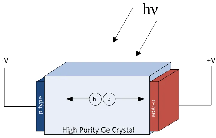
When radiation is incident on the Ge crystal, electron-hole pair is produced. Since the detector is biased in depletion mode, the large electric field will attract the generated charged particles to their respective electrodes, where the particles are collected, and registered by the external circuitry.
Main disadvantage of this type of detector is that lithium can easily diffuse into the crystal at room temperature, which degrades the contact. To prevent the degradation of the electrode, the detector must be operated at 77K, which limits the “lifetime, operating, storing, and transporting detectors” [10].
Figure 9 Depiction of the functionality of Ge crystal-based sensor. A p-type
Cadmium Zinc Telluride (CZT)
The cooling of Germanium crystals has proved to be a difficult obstacle to overcome for applications outside of laboratory, and accelerator settings. This led the researchers to look for new materials with the capability to measure radiation at room temperature. For these purposes, Cadmium Telluride (CdTe), and Cadmium Zinc
Telluride (CZT) are viable materials because they are direct band gap material with very high resistivity to reduce the leakage currents, which are among the primary requirements for a suitable semiconductor for radiation sensing [13]. Fabrication of either CdTe or CZT begins with the creation of CdTe crystals, and uses dopants to achieve the required properties. Chlorine is used as the dopant in CdTe, and Zinc in the fabrication of CZT. The addition of Zinc increases the bandgap of the material [14]. The following table summarizes the comparison between CdTe, and CZT.
Table 2 Comparison between CdTe, and CZT (with 10% Zn) [14]
Characteristics CdTe (Cl) CZT
Bandgap (eV) 1.47 1.65
Mobility ( e: 1000-1100
h: 80
e: 1000-1100 h: 50 Resistivity (Ω•cm) 1-3 x10⁹ 0.5-1 x10¹¹ Operating Electric Fields
Figure 10 CdTe-ZnTe phase diagram [15]. The formation of these crystals with different molar fractions of ZnTe is illustrated in this figure. Increasing the molar quantity of ZnTe increases the liquidation temperature, but the incorporation of Zn enhances the crystal characteristics as shown in Table 2.
Figure 10 represents the liquidus, and solidus curve for a melt containing various compositions of CdTe, and ZnTe. The upper curve in the figure corresponds to the melting temperature of the material, while the bottom curve represents the temperature of crystallization for different mole fractions of ZnTe within the CdTe. There are different methods to create CZT crystals, of which high pressure (HP), low pressure (LP)
these two melts are reacted together at the melting temperature. At this point of the growth process, dopants such as Zinc, and Chlorine are introduced into the melt [17]. To generate crystals, the liquid alloy is slowly cooled, which produces the final crystals. Growth of crystals requires either the temperature to be greater than 1100 ºC or a high pressure as described in the pressure vs. temperature graph shown by Su, and Lehoczky [18]. The crystals must be crack free, defect free, and highly homogenous; otherwise, the process must be restarted until high-quality crystals are achieved. The entire process is highly expensive, and has a very low yield, therefore this reflects the cost, and the availability of such crystals.
The fabricated crystals can either be p-type or n-type conductive material depending on the growth process of the crystals [19]. Detector properties can be optimized by engineering the Fermi level to make the material have n-type conductive properties since the lifetime of the carriers is greater, but this in turn reduces the
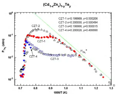
Figure 11 Pressure vs. Temperature curve for different compositions of CZT [17]. The large melting temperature for the formation of CZT crystals can be mitigated by increasing the pressure within the melt chamber, thus effectively reducing the required temperature. Effective crystals have been formed at 769 K as shown in the graph above.
electron is invisible. This would not be a big problem for p-type material with the capability to capture the electron, and affect the conductivity of the material.
Recent developments in the field of radiation sensors have allowed the creation of an easily transportable CZT detector. The group of Luke et al. have created a small “Pocket-size” detector with a 2 cm3 volume CZT sensor with all self-enclosed
components to detect radiation [20]. Package consists of a high voltage source, power converters, and a separate segment of the circuit board dedicated to the digital, and analog circuit components [20].
CHALCOGENIDE GLASSES, AND RADIATION-INDUCED EFFECTS
Chalcogenide Glasses (ChG) are a segment of materials that are considered as amorphous semiconductors. These materials have been researched for various
applications such as memory, photolithography, chemical sensing, as well as radiation sensing [21, 22]. Compared to the other possible applications for ChG, radiation sensing is a very novel, and promising research area because of the range of structural changes that are possible, and the lack of research in this aspect.
Basics of Glasses
All materials are classified in one of four forms based on entropy, and structural order. The materials with the highest entropy are either gasses or plasma while the lowest entropy characteristic for solids. Solids consist of three main groups of materials, which are single crystalline, poly crystalline, and amorphous. Single crystalline materials have high range order with the exception of very few defects. The atoms are arranged in a distinct pattern of periodically repeated unit cells, for example, single crystalline Si. Poly crystalline materials on the other hand have the benefits derived from the single
crystalline structure with the addition of grain boundaries. These types of materials have multiple crystalline structures separated by boundaries, which has specific benefits, for example, the use of poly crystalline Si as a gate electrode in CMOS technology.
are an example of materials with such characteristics that are direct result of the production of glasses. Glasses are conventionally produced using the melt quench technique, which begins by taking measured amounts of pure elements in pellets or powder form, corresponding to a specific composition, sealed inside evacuated ampoules. The next procedure is to place the sealed ampoule into a specialized furnace, which raises the temperature until all the materials are in molten liquid form. At this point, the furnace is rocked to ensure complete mixture of all the elements. This step is followed by a quick quench to solidify the mixture but also maintaining the amorphous nature of the glasses by freezing the equilibrium characteristic of the liquid mixture. This process is
summarized in the following figure, which shows the temperature as a function of viscosity.
Figure 13 Temperature vs. Viscosity for formation of glasses. The material that
will be used to form glasses is placed in an ampoule, and the temperature of the
ampoule is increased in stage 1. Once the melting temperature (Tm) of the material
is achieve at stage 2, the viscosity of the material greatly increases. The molten melt
is set to achieve a quenching temperature (TQ), which is followed by removing the
molten material, and quenching in air or ice bath in step 4, transitioning into step 5
at the glass transition temperature (TG). At step 5, a glass is formed that has a
becomes a liquid. After reaching the molten state, in step 3, the molten liquid is removed from the furnace, and is immediately quenched in air, water, or ice bath, depending on the required quench rate. When the molten alloy is quenched at a fast rate (step 4), then the resultant material is in glass form, and the viscosity of the material is higher than the viscosity of the initial material. The characteristic temperature for the transition from liquid to solid state is called glass transition temperature (TG). Slow cooling rate will
follow the dotted line in Figure 13, and reach a similar viscosity of the original material, therefore achieving a crystalline structure by which the material will reach its equilibrium state. Crystalline material has the lowest entropy, therefore if the system is allowed to slowly cool, the atoms can form a structured order, but a fast cooling rate prevents the material from achieving this molecular organization. The primary concern for glasses is to ensure the temperature of the glass is sufficiently lower than the glass transition temperature. When the temperature of the glass begins to approach the glass transition temperature, the glass will begin to liquefy, and without the proper cooling rate, material could become semi crystalline, which has completely different properties than the amorphous glass.
theorized by Phillips [23]. According to this theory, ideally the compositions with mean coordination number of 2.4 can easily form glasses. This ideal mean coordination number creates a situation where the number of constraints per atom is equal to the degrees of freedom for each atom. Mean coordination number can be calculated using the following equation for an arbitrary alloy with elements A, and B, in a compound AxB100-x.
( 21 )
Where ZA is the coordination number or the number of additional valance
electrons that are required to satisfy the 8-N rule for element A, and similarly ZB is the
coordination number of element B. For example, the mean coordination number for Ge20Se80 is 2.4. Further research into the relationship between the glass formation
regions, and the mean coordination number revealed that structural properties are also correlated to the coordination number. It was shown by M. Thorpe that r =2.4 is the transition point from floppy (r < 2.4) to rigid (r > 2.4) structure of the glasses [24-28]. When a structure is floppy, it means that there is greater degree of flexibility between bonds, resulting in an overall flexible glass, while rigid structure have considerably less freedom. Floppy structures are primarily chalcogen-rich glasses. Recently, P. Boolchand has stated that in addition to the floppy, and rigid glass phases, there exists an
intermediate phase where the glasses are non-stressed rigid, and they do not age [29-32]. Hence, using the bond constraint theory, information about glass formation region, and structural properties of glasses, compositions can be used to determine the purpose, and application of said glasses.
the structural is minimal at this composition [29, 33-35]. This transition is shown in the figure below for various chalcogenide glasses, which is a comparison between the coordination numbers to the non-reversing heat-flow parameter.
Figure 14 DSC measurements for various GexSe1-x, and SixSe1-x compositions
showing the transition from floppy-intermediate-rigid structure [31]. The application of Differential Scanning Calorimetry expounded that in addition to the floppy, and rigid phases, there is a transition region, which is classified as the intermediate phase.
It was also mentioned that the glasses described as floppy, and rigid are known as “fragile liquids” while the glasses in the intermediate phase are shown to have
characteristics described as “strong liquids” [29, 33]. These classifications are derived from the connectivity within the system.
Figure 15 Raman shift of CS units versus Pressure for various GexSe1-x [23].
glasses to other glassy material is the inclusion of group VI elements such as Sulfur (S), Selenium (Se), or Tellurium (Te) within the composition of the glass alloy. These three elements are also known as chalcogen elements, and thus glasses created from these elements are known as chalcogenide glasses. Chalcogenide glasses range from glasses created with only S, Se, or Te to binary compounds, which consist of other elements in combination with the chalcogen elements to more complex alloys, with the only requirement being the presence of at least one of the chalcogen atoms in the glass composition. There is no end to the possible compounds that can be created, and each combination is used for a specific purpose because of the structure, the bonding between the elements, and properties of each unique combination.
Glass formation, and phase diagrams are an important method of studying the properties of chalcogenide glass. The formation of glasses using chalcogen elements has been researched, and a specific trend has been determined between the different
chalcogen atoms. Elemental Sulfur can be alloyed into a glass when heated to a
temperature greater than 160ºC, and then quenched at -27ºC [36]. Selenium has a TG of
40ºC, but tellurium cannot form a glass [36]. This data follows the general trend for glass formation capability of chalcogenide glasses, where selenium has the largest ability followed by sulfur, and tellurium has the smallest ability. The glass formation capability of chalcogenide glasses is highly dependent on their connectivity. For example,
Figure 16 Phase diagram of Ge containing chalcogenide glasses (a) S, (b) Ge-Se, and (c) Ge-Te [36].
Study of phase diagrams reveal an abundance of information from melting temperature, and glass formation region for various compositions of a specific binary glass compound. The phase diagrams for Germanium (Ge) containing glasses show GexS1-x (10 at.%≤ x ≤ 47.6 at.%), GexSe1-x (0 at.% ≤ x ≤ 40 at.%), and GexTe1-x (12at.%≤
The availability of lone pair electrons, and the mixture between the covalent, and van der Waals bonding between the elements in the chalcogenide glasses gives rise to the photoinduced effects within these materials. In the following sections, chalcogenide glasses have been characterized using two types of photons (sub-bandgap light, and gamma rays), which will be discussed in detail, and their structural changes, as well as the photon effects on the optical properties of chalcogenide glasses.
Sub-Bandgap Light
Structural Changes
Prior to discussing the structural changes induced by sub-bandgap light, it is important to discuss the properties of the chalcogen atoms since these atoms determine the unique properties of these types of glasses. Sulfur, Selenium, and Tellurium as a group have specific properties that are characteristically unique in the world of glasses, but each of these elements vary in their own unique manner. The sizes of the atoms increase from Sulfur to Selenium to Tellurium, and this is inversely proportional to the bond strengths of atoms. For example, Te-Te bonding is weaker than Se-Se bonding, and in turn weaker bonding energy than S-S. This pattern is similar for the bonding energy of some combinations of chalcogen atom with other elements for the prominent
Table 3 Bond energies for common atomic bonds in Chalcogenide glasses [37]
Another pattern that arises from the bonding energies is the thermal stability of the glasses. Glasses containing Te have the lowest Tg, and this transition temperature
increases to sulfur containing glasses in the following manner: S > Se > Te.
Chalcogen atoms have two electrons in the s shell, and four in the p shell. Two of the s-shell electrons, which have opposite spins, will bond with each other. The p-shell electrons are the reason chalcogenide glasses are highly researched because the electrical, and optical capabilities are derived from these electrons. Two of the p-shell electrons will become lone pair electrons forming an electron pair, and the other two electrons will covalently bond with other atoms. When glasses are created with only chalcogen atoms, the following unique properties were discovered, which will be explained individually.
Figure 17 Two location for sulfur atoms within a sulfur chain a) cis and b) trans.
Crystalline sulfur forms orthorhombic chains with 8 sulfurs with a trans configuration at bond angles of 105º. This orthorhombic structure is shown below.
Figure 18 Orthorhombic sulfur rings S8 a) side view and b) front view.
In sulfur-rich glasses, the sulfur rings can phase separate from the remainder of the glass network, which is the main reason for the smaller glass formation region in comparison to the selenium atoms. Additionally, sulfur has as significantly higher partial pressure, which is an attribute that is unique to sulfur containing glass in contrast to the other two chalcogen-containing glasses.
Figure 19 Hexagonal Selenium chains a) configuration of the chains and b) top view of the chains.
Similar to Selenium, Tellurium also forms long spiraling hexagonal chains held together with Van der Waals forces [39]. These chains are shown in the figure below.
Figure 20 Tellurium chains a) configuration of the chains and b) top view of the
chains.
Telluriums is considered as a semi-metal, and has characteristics similar to metals, such as having a very narrow bandgap, high conductivity, and are lustrous in appearance.
transition between the VB, and occupy a state in the CB, the electron must acquire sufficient energy to overcome the band gap energy. Ideally, in these materials, the Fermi level, which provides information on whether there is an abundance of holes or electrons within the material, is situated in the middle of the band gap, suggesting similar number of electrons, and holes at 0 K or ideally intrinsic (undoped) semiconductors.
Chalcogenide glasses on the other hand, have band tail states, and localized states along with the two band states [40-42]. These extra states are attributed to the presence of lone pair electrons as well as the amorphous structure of the glasses. The localized states between the CB, and VB are primarily due to the presence of the lone pair electrons, while the band tail states are attributed to the Van der Waal’s forces between layers of atoms [43]. Localized states are trap locations within the band gap where electrons from the valence band can hop into, on their path towards the conduction band. Tail states on the other hand are locations near the band gap, and are known as Urbach tail states. These states are occupied with many electrons that can participate in the various changes due to interaction with photons. The investigation by Utsugi and Mizushima stated that electron-phonon interactions are responsible for the generation of the Urbach tails [44-46]. The Urbach tail states are responsible for setting the absorption edge for glasses, and photons with energy near the band gap affect these states.
Optical Properties

![Figure 2 Relates the photon energy to the atomic number of the material, showing the regions where each type of effect is prevalent [3]](https://thumb-us.123doks.com/thumbv2/123dok_us/8921937.1842371/36.612.132.495.70.317/figure-relates-photon-energy-material-showing-regions-prevalent.webp)

![Figure 8 Change in voltage pulse due to collection of electron, and positive ion Influx of a greater number of radiation photons creates large number of ions, [5]](https://thumb-us.123doks.com/thumbv2/123dok_us/8921937.1842371/45.612.213.436.76.277/figure-change-collection-electron-positive-radiation-photons-creates.webp)
![Figure 10 CdTe-ZnTe phase diagram [15]. The formation of these crystals with different molar fractions of ZnTe is illustrated in this figure](https://thumb-us.123doks.com/thumbv2/123dok_us/8921937.1842371/50.612.146.500.70.351/figure-diagram-formation-crystals-different-fractions-illustrated-figure.webp)


![Figure 21 Absorption edge of a-Selenium [48].](https://thumb-us.123doks.com/thumbv2/123dok_us/8921937.1842371/67.612.203.450.362.665/figure-absorption-edge-of-a-selenium.webp)
