University of New Orleans University of New Orleans
ScholarWorks@UNO
ScholarWorks@UNO
University of New Orleans Theses and
Dissertations Dissertations and Theses
12-17-2010
Highly Sensitive and Selective Gas Sensors Based on Vertically
Highly Sensitive and Selective Gas Sensors Based on Vertically
Aligned Metal Oxide Nanowire Arrays
Aligned Metal Oxide Nanowire Arrays
Jiajun Chen
University of New Orleans
Follow this and additional works at: https://scholarworks.uno.edu/td
Recommended Citation Recommended Citation
Chen, Jiajun, "Highly Sensitive and Selective Gas Sensors Based on Vertically Aligned Metal Oxide Nanowire Arrays" (2010). University of New Orleans Theses and Dissertations. 106.
https://scholarworks.uno.edu/td/106
This Dissertation-Restricted is protected by copyright and/or related rights. It has been brought to you by ScholarWorks@UNO with permission from the rights-holder(s). You are free to use this Dissertation-Restricted in any way that is permitted by the copyright and related rights legislation that applies to your use. For other uses you need to obtain permission from the rights-holder(s) directly, unless additional rights are indicated by a Creative Commons license in the record and/or on the work itself.
This Dissertation-Restricted has been accepted for inclusion in University of New Orleans Theses and Dissertations by an authorized administrator of ScholarWorks@UNO. For more information, please contact
Highly Sensitive and Selective Gas Sensors Based on Vertically Aligned Metal Oxide Nanowire Arrays
A Dissertation
Submitted to the Graduate Faculty of the University of New Orleans in partial fulfillment of the requirements for the degree of
Doctor of Philosophy in
Engineering and Applied Science Physics
by
Jiajun Chen
M.S. University of Electronic Science and Technology of China, 2004 B.S. University of Electronic Science and Technology of China, 2001
c
Dedication
Acknowledgments
The research of this dissertation was conducted during my Ph. D program at Advanced
Ma-terials Research Institue (AMRI), University of New Orleans (UNO). Without the enormous help
from the colleagues of AMRI, UNO and other institutes, this research is impossible.
I would like to express my greatest gratitudes to my advisor, Prof. Weilie Zhou, for his expertise
in this field, and his continuous support and insightful advice in my Ph. D research and as well my
life.
I want to thank the academic committee members: Prof. Kevin Stokes, Prof. Leszek Malkinski,
Prof. Ashok Puri, and Prof. Paul Schilling for their helpful suggestions on this dissertation.
I would like to thank Dr. Baobao Cao, Mr. Kai Wang for their important support of materials
syntheses; I would like to thank Drs. Zhongming Zeng, Zengxing Zhang, Kun Yao, and Mr. Renhai
Long for the valuable discussion in electrical measurements and nanolithography.
I am greatly thankful to Dr. Yanfa Yan in National Renewable Energy Laboratory for allowing
us to use their advanced field emission electron microscopes and providing precious technical
supports on nanostructure study.
I am deeply indebted to Prof. Zhonglin Wang’s group in Department of Materials Science
and Engineering, Georgia Institute of Technology for hosting me as a transient student during
distraction aftermath of Hurricane Katrina. Without their help, it is impossible for me to continue
my research and study.
I would like to thank AMRI for continuous support of graduate assistantship during my Ph.D
program. I gratefully acknowledge the financial supports from the DARPA Grant Nos.
HR0011-07-1-0032 and HR0011-04-1-0029 and the Louisiana Board of Regents Contract No. LEQSF
Contents
Abstract viii
1 Introduction 1
1.1 The Momentum of Nanotechnology . . . 1
1.2 Modern Electronic Gas Detection . . . 4
1.2.1 Electronic Gas Detection Methods . . . 5
1.2.2 Metal Oxide Conductometric Gas Sensors . . . 9
1.2.3 Factors Affecting the Sensing Performance . . . 14
1.2.3.1 Effects of Crystalline Size . . . 14
1.2.3.2 Effects of Catalytic Noble Metals . . . 15
1.2.3.3 Other Factors . . . 17
1.2.4 Metal Oxide Nanowire Gas Sensors . . . 19
1.3 Biological Olfactory System and Electronic Noses . . . 19
1.4 3D Metal Oxide Nanowire Arrays for Gas Detection . . . 23
1.4.1 Vapor-phase Growth of Metal Oxide Nanowire Arrays . . . 24
1.4.2 Solution Synthesis of Metal Oxide Nanowire Arrays . . . 28
1.5 Objectives of the Dissertation . . . 32
2.1.1 Background . . . 34
2.1.2 Growth of Monoclinic WO3Nanowire Arrays and Gas Senor Fabrication . 35 2.1.3 Sensing Performance of Gas Sensors Based on Monoclinic WO3Nanowire Arrays . . . 38
2.1.4 Summary . . . 41
2.2 CuO Nanowire Array Sensor Prepared byIn-situManipulation . . . 42
2.2.1 Background . . . 42
2.2.2 Fabrication of CuO Nanowire Array Gas Sensors byIn-situManipulation . 43 2.2.3 Sensing Performance of CuO Nanowire Array Gas Sensors . . . 46
2.2.4 Summary . . . 52
3 Electronic Noses Based on Multiple Nanowire Arrays 54 3.1 General Route to the Growth of Metal Oxide Nanowire Arrays . . . 54
3.2 Effectiveness of Template Growth of Metal Oxide Nanowire for Gas Sensing . . . 56
3.2.1 Preparation of Pd/SnO2-coated ZnO Nanowires . . . 56
3.2.2 Sensing Performance of Single-Nanowire Devices . . . 61
3.2.3 Summary . . . 66
3.3 Gas Discrimination by Electronic Noses Based on Multiple Nanowire Arrays . . . 66
3.3.1 Electronic Nose Prepared by Nanowire Arrays with Different Metal Oxide Coatings . . . 67
3.3.1.1 Fabrication of ZnO Nanowire Arrays with SnO2and CuO Coatings 67 3.3.1.2 Electrical Properties and Sensing Performance of Metal Oxide Coated ZnO Nanowire Arrays . . . 71
3.3.1.3 Summary . . . 74
3.3.2.2 Gas Sensing and Discrimination by SnO2coated ZnO Nanowire
Arrays with Different Catalytic Metal Coatings . . . 77
3.3.2.3 Summary . . . 87
4 Conclusions and Future Perspectives 88
Appendices 90
A Gas Sensor Testing System Used in This Dissertation 91
B Data Extracted from a Responsive Curve of Gas Sensor Testing 93
C Principle Component Analysis 95
D Copyright Permissions 97
References 107
Abstract
Mimicking the biological olfactory systems that consist of olfactory receptor arrays with large
surface area and massively-diversified chemical reactivity, three dimensional (3D) metal oxide
nanowire arrays were used as the active materials for gas detection. Metal oxide nanowire
ar-rays share similar 3D structures as the array of mammal’s olfactory receptors and the chemical
reactivity of nanowire array can be modified by surface coatings. In this dissertation, two
stan-dalone gas sensors based on metal oxide nanowire arrays prepared by microfabrication andin-situ
micromanipulation, respectively, have been demonstrated. The sensors based on WO3 nanowire
arrays can detect 50 ppb NO2 with a fast response; well-aligned CuO nanowire array present a
new detection mechanism, which can identify H2S at a concentration of 500 ppb. To expand the
material library of 3D metal oxide nanowire arrays for gas sensing, a general route to
polycrys-talline metal oxide nanowire array has been introduced by using ZnO nanowire arrays as structural
templates. The effectiveness of this method for high performance gas sensing was first investigated
by single-nanowire devices. The polycrystalline metal oxide coatings showed high performance
for gas detection and their sensitivity can be further enhanced by catalytic noble metal
decora-tions. To form electronic nose systems, different metal oxide coatings and catalytic decorations
were employed to diversify the chemical reactivity of the sensors. The systems can detect low
concentrated H2S and NO2 at room temperature down to part-per-billion level. The system with
different catalytic metal coatings is also capable of discriminiating five different gases (H2S, NO2,
NH3, H2and CO).
Chapter 1
Introduction
1.1 The Momentum of Nanotechnology
Nanotechnology is a multidisciplinary field, which spans over various basic science and
engi-neering areas. The earliest arise of the term “nano-technology” should be dated back to the year
of 1956, when Prof. Richard Feynman in California Institute of Technology presents the famous
talk “There’s Plenty of Room at the Bottom” [1]. He described the possibility of manipulation of
individual atom or molecule, the new phenomena in the confined scales and the bright future to
ex-pand the functionality of various tools. After that, new discoveries in nanoscale, such as quantum
confinement effect [2], fullerene [3], carbon nanotube [4, 5], and graphene [6], had generated lots
of interest in the nanotechnology. The Clinton’s administration elevated the nanoscience and
nano-technology as a federal level initiative, referred as National Nanonano-technology Initiative (NNI) [7], in
2001 when the research in nanotechnology started to pick up its momentum in various disciplines.
Significant advances have been made in the last decade both in fundamental science research and
the applications of nanotechnology. Figure 1.1 gives publication numbers with keyword of
“nano-technology” in last 20 years. The number of related publications have been increase at least 10
times from the year of 2001 to 2009, implying tremendous research efforts have been put into this
area and this trend will be maintained.
There are two major properties of nanomaterials that are employed in many applications of
Figure 1.1: Number of publications with the keyword “nanotechnology” in last 20 years, acquired from ISIknowledge website.
briefly introduced. As the feature size of nanomaterials reduces to less than 10 nm, the condition of
periodic energy wells in a crystal may be broken down in one or more dimensions and the boundary
effects must be considered. The nanomaterials can be divided into four different categories in terms
of the confinement of dimensionality, which are shown in Figure 1.2. The representative plots of
their corresponding density of states (DOS) are given on the left side. For the nanomaterials (e.g.
quantum dots, nanowires, 2-dimensional electron gas) in which the electrons are confined in at
least one direction, discreted energy level may arise and the energy band gaps may also deviate
from their bulk counterparts. One famous example with commercialized applications [8] (e.g.
biological labeling, light emitting diodes, photovoltaics, etc.) is the semiconducting quantum dots
with emission wavelengths that can be adjusted through their sizes. However, the feature size of
Figure 1.2: The diagrams and representative plots of density of states (DOS) of confinement nano-materials: (a) 0D, namely a single energy well with barriers along all three directions; (b) 1D, quantum wire; (c) 2D, electron wave function are limited in a two-dimensional layer; (d) bulk materials. After Ref. [9].
is applausible.
Another important properties for nanomaterials is the large surface-to-volume ratio, which
means nanomaterials consist more precentage of surface atoms as the feature sizes decrease.
Fig-ure 1.3 plots the percentage of surface atoms with respect to the nanoparticle diameters,
show-ing the inverted proportional relationship between them, showshow-ing that the percentage of surface
atoms significantly increases as the particle diameter decreases, especially when the diameter is
less than several tens of nanometers. The inset is a schematic comparing the surface atoms in
spherical particles with different diameters. Generally, surface atoms have much higher reactivity
than the bulk (inner) atoms of a particles due to the suspended (dangling) chemical bonding. This
is why nanometerials are generally have higher reactivity than bulk materials. For instance, the
performance of Pt catalytic nanoparticles can be significantly enhanced when the particle size is
reduced. And further, the large surface-to-volume ratio can also alter the fundamental properties
Figure 1.3: Plot of percentage of surface atoms in terms of the diameter of a spherical nanoparticles with close-packed structure, showing the inversely-proportional relationship. The insets are two schematics showing how the sphere diameters affect the surface-to-volume ratio.
Nanotechnology has infiltrated into many scientific areas and enabled numerous novel
appli-cations, such as biological labeling [10], drug delivery [11], renewable energy [12], environmental
monitoring [13], electronics [14], etc. Among all these applications, nanomaterials and
nanode-vices for gas sensing is one of the most important aspects of nanotechnology with promising future
of real world applications, which is also the central topic of this dissertation.
1.2 Modern Electronic Gas Detection
Gas sensor is one of the most important modern electronic components, which has obtained
(e.g. photo-diode, charge-coupled device (CCD), microphone or sonar detector), gas sensors play
a role of interface between environment and electronic systems. Gas sensors can discriminate
some specific chemical vapor molecules that present in environment, evaluate their concentration
and monitor their change. Based on the enormous performance increase, gas sensors currently
have various critical applications, such as public safety, environmental monitoring, food industry,
aerospace, automobile, etc [16, 17]. For examples, gas sensors have been employed to monitor the
product quality in perfume industry, and toxic gas detectors can be used for environment evaluation
before workers enter some dangerous work places. Recent development in technology and
appli-cations has imposed more and more strict requirements on the performance of gas sensors. The
development of mobile devices, high-speed wireless networks, and geographical positioning
sys-tem (GPS) makes the massively distributed environment monitoring syssys-tem become possible [18],
which require the sensing devices to have small form-factors and extremely low power
consump-tion [19]. Addiconsump-tionally, highly sensitive and selective gas sensors with fast response are needed
for applications in public safety. These requirements triggered enormous research efforts in the
development of high performance gas detection devices. The application of nanomaterials and
nanotechnology is a major route to meet these demands. In the following sections, the general
electronic gas detection methods will first be introduced, and then we will focus on the detection
mechanism of metal oxide conductometric gas sensors and the applications of nanotechnology in
metal oxide gas sensors.
1.2.1
Electronic Gas Detection Methods
To analyze the gas contents in the atmosphere, one needs to detect the variation in physical or
chemical properties of the environment when the interested gases present or absent, for examples,
electrical conductivity, photo-luminescence, and gas diffusion coefficient have been employed as
the media to identify specific vapor molecules [17, 20, 21]. Many of these gas sensors have already
based on electrical detection methods, while other special gas detection schemes, such as mass
spectrometers, gas chromatograph, or optical sensors, will not be covered since electrical detection
are the most promising methods to simultaneously address concurrent demands of gas detection
-low power consumption, portable, high sensitivity and stability, etc.
Electrochemical Sensors. The operation of an electrochemical sensor relies on the oxidation
or reduction of gas molecules at the surface of sensing electrode where an electrical signal
propor-tional to the gas concentration is generated. Figure 1.4(a) shows the detection mechanism of an
electrochemical sensor. A hydrophobic membrane is generally used in a real sensor to avoid the
electrolyte leaking and allow the gas molecules to diffuse into the device. The electrical current
flow through the circuit is proportional to the gas concentration, which can be easily picked up by
a current meter. Thus, this type of gas sensors is also named as amperometric gas sensors. Because
the electrical current is generated from the reaction and generally no heating element is needed,
electrochemical sensors have the lowest power consumption among all kinds of gas sensors.
How-ever, electrochemical sensors show relative poor selectivity, which can be improved by the use of
a chemical filter.
Catalytic Combustible Gas Sensors. Catalytic combustible gas sensors are also called as
“cat-alytic bead detector” due to their bead-shape cat“cat-alytic metal oxide compounds. A platinum coil
goes through the catalytic bead, which work as the heating wire and the resistive sensors, as
shown in Figure 1.4(b) [22]. The ignition temperature is generally very high for most combustible
gases (>1000◦C), while the catalytic bead can effectively reduce the ignition temperature down to
500◦C. The combustion reaction increase the temperature of the platinum wire and thus change the
resistance of the wire. The resistance change can be monitored by electronic meter. The catalytic
combustible gas sensors are easy to manufacture but pull large power consumption due to the high
working temperature.
Surface-Acoustic-Wave (SAW) Gas Sensors. Figure 1.4(c) provides the diagram of a typical
Figure 1.4: Schematic diagrams of electronic gas sensors based on different detection mecha-nisms: (a) electrochemical sensors; (b) catalystic combustible gas sensors; (c) surface-acoustic-wave (SAW) gas sensors; (d) cantilever gas sensors; (e) solid-state conductometric gas sensors; (f) Zirconium oxide oxygen sensors.
sensing membrane. A high frequency signal is applied onto the input transducer, in which the
piezoelectric film generates a SAW across the sensing layer. After propagating through the sensing
layer, the SAW is picked up by the output transducer. The propagation velocity of SAW in the
sensing layer is changed when the device is exposed to the targeting gases. By monitoring the
phase difference between the input and output signal, the concentration of targeting gases can
be evaluated. The most important benefit of using SAW is its slow propagation speed compared
with electromagnetic waves, which allows the preparation of miniaturized sensors working at high
frequency and provides fast responses.
Cantilever Gas Sensors. Micro-cantilever is a thin film beam freely suspended above the
de-vice substrate, which is generally prepared by microfabrication in microelectromechanical systems
mate-rials, geometrical factors, and the environment. A sensing layer can be applied onto the cantilever
for gas molecule detection [Figure 1.4(d)]. The resonant frequency of the cantilever changes due
to the mass increment caused by gas absorption. Frequency measurement is generally more
ro-bust than current or voltage measurement and show strong capability to resist background noise.
Biological sensing layer, such as deoxyribonucleic acid (DNA), enzyme, or protein, can be
em-ployed for bio-detection and the cantilever can be easily adapted into devices that operate liquid
phase media. The fabrication of cantilevers are relatively complex and requires well-controlled
processings.
Solid-State Conductomentric Gas Sensors. Solid-state conductometric gas sensors consist of
two metal electrodes through which the conductivity or resistivity of the materials is continuously
measured. The active sensing materials can be in the forms of bulk, thin or thick films. Various
materials have been used as the active materials, such as metal oxides [28], conducting polymer
[29–31], graphene [32], carbon nanotubes (CNTs) [33] etc. The adsorbed gas molecules at the
material surface or interface alter the electronic structures and result in conductivity change. The
detailed detection mechanism and factors that influence the sensing performance will be discussed
in the following section. The structure of conductometric gas sensors is relatively simple and
very convenient for large scale production and they also show very high sensitivity and selectivity.
Additionally, many different methods can be used for sensitivity tunig, which enable construction
of more complex gas detection systems — electronic noses.
Zirconium Oxide Oxygen Gas Sensors. This type of gas sensors is widely used in automobile
vehicle, in which the gas sensor monitors the oxygen content in the engine emission and feedback
the measurement to the controller computer for efficient fuel combustion in the engine. Similar to
solid-state conductometric sensors, ZrO2 sensors are also two terminal devices, shown in Figure
1.4(f). The porous catalytic platinum electrodes are applied on the both sides of ZrO2 ceramics.
The platinum electrodes not only work as electrical connections but also help to dissociate the
of oxygen ions. The difference in oxygen partial pressure between both sides of the ZrO2ceramics
induces a Nernst voltage, which can be measured across the electrode elements. The device works
at high temperature and provide fast response, however this high temperature also brings up some
problems. For instance, the temperature is so high that almost all the combustible gases can be
ignited, which creates interference signals. The device is majorly used for monitoring the waste
gas emissions and is not suitable for portable applications.
Other than the above-mentioned detection methods, research groups are also developing new
phenomena for gas sensing applications. Piezoelectric metal oxides have been used to detect the
swell in organic polymer when they were exposed to organic vapors [34, 35] and the effect of gas
environment on the Schottky barrier at the metal-semiconductor interfaces also showed very high
sensitivity towards some specific gas molecules [36, 37]. The metal-insulator-transition (MIT) in
vanadium oxide was also employed for gas detection [38, 39]. Though these sensors only
demon-strated in the laboratory, most of them present the quality of high sensitivity and low power
con-sumption, implying possible applications in high performance integrated systems.
1.2.2
Metal Oxide Conductometric Gas Sensors
As described in previous section, various phenomena can be used for gas detection. Among
all these detection methods, metal oxide conductometric gas sensor is one of the most promising
techniques that can meet the modern demands for integrated gas detection system due to their
properties of low production cost, low power consumption, high sensitivity and stability [15, 40].
The metal oxide conductometric gas sensors detect gases by measuring the variation of
resis-tance or conducresis-tance of the metal oxide materials. The mechanism of the change in conductivity
is generally explained by the absorption and desorption processes of oxygen species on the
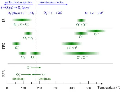
semi-conducting metal oxide surfaces [41]. Figure 1.5 provides experimental results of oxygen species
adsorbed on the SnO2 surfaces. It was found that molecule-ion species (O−2 or O2−2 ) dominated
Figure 1.5: Oxygen species adsorbed on the SnO2 surfaces analyzed with different methods: in-frared (IR) analysis, temperature programmed desorption (TPD), electron paramagnetic resonance (EPR). After Ref. [41].
temperature. Though the transition temperatures given by different measurement techniques are
different, the basic trends of this phenomenon are similar. The adsorbed oxygen species may form
surface states that trap electrons from the semiconducting metal oxide creating a surface charge
de-pletion layer that possesses high resistance. Therefore, it is possible to connect the conductivity of
metal oxide with the coverage of oxygen species on its surfaces. Barsan et al. [41] have proposed
a conduction model to relate the electrical conduction of metal oxide semiconductor with oxygen
can be given as
β 2O
gas
2 +α·e
−+S
O−α
βS (1.1)
where Ogas2 is oxygen molecule in the enviroment;e− is an electron that can reach the metal oxide
surface; S is the surface sites that can accept oxygen species. And α and β are integers that
determine the type of oxygen species, for example, α =1 means the oxygen species are singly
ionized and β =2 means they are molecular form. By using the mass action law of Eq.1.1, one
can deduce the relationship of concentrations of reactants and products:
kads·[S]·
e−α·pβO/2
2 =kdes·
h
O−α βS
i
(1.2)
wherekadsandkdesare the reaction constants for oxygen absorption and desorption processes. The
total number of surface sites for oxygen absorption including occupied ones is donated as[St], and
the surface coverageθ is given asθ =
h
O−α βS
i
/[St]. Thus, the Eq.1.2 can be rearranged by using
the implied relation[S] +hO−α βS
i
= [St]:
(1−θ)·kads·
e−α·pβO/2
2 =kdes·θ (1.3)
Eq.1.3 has created a relation between the surface coverage θ and the concentration of electrons
that can reach to the surface [e−]. However, more equations are needed to connect the electron
concentrations with the oxygen partial pressure in atmosphere. The situation is similar to
Schot-tky approximation [42] where the conditions of electroneutrality and carrier distribution based on
Poisson equations were used. Once the geometry of the metal oxide crystal is defined, the relations
between the electron density and the oxygen pressures can be obtained.
Discussion above has shown how the surface adsorbed oxygen species deplete the electrons
close to the metal oxide surface creating a surface charge depletion layer. To further clarify the
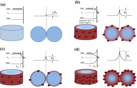
Figure 1.6: Schematics of relationship between oxygen adsorbates and the surface depletion layer on metal oxide wires or particles usingn-type semiconductor as an example. (a) The energy bands and contact barrier for pristine metal oxides. (b) Metal oxides adsorb oxygen from atmosphere forming surface charge depletion layer. (c) Adsorbed oxygen species react with reducing gases and release trapped electrons back to metal oxide, which decreases the thickness of depletion layer. (d) Oxidizing gases trapped more electrons from metal oxides and enhance the depletion layer.
analyze the effect of surface reactions on the overall conductivity. Figure 1.6 shows several typical
states and surface energy band diagrams of metal oxides when they are exposed to different
am-bient atmosphere. Considering that the metal oxide is in a realistic vacuum where no gas species
are adsorbed, the carrier density on the whole material is homogeneous and there is a contact
bar-rier between adjacent particles, which contributes the major part of the devices resistance [Figure
1.6(a)]. As the device exposes to the atmosphere, the oxygen species attach to the metal oxide
process results in electron lost in the surface layer. The width of charge depletion layer is defined
as Debye length, LD. The build-up of depletion layer increases the particle-to-particle contact
barriers and decrease effective cross-section for electron transport in metal oxide bulk, shown in
Figure 1.6(b). When exposed to reducing gas molecules, such as H2S, CO, NH3, H2 etc., the
adsorbed oxygen species react with these gases and release the electrons back to the metal oxide
semiconductor:
H2+O−→H2O+e, CO+O−→CO2+e,
2NH3+3O−→3H2O+N2+3e, H2S+3O−→H2O+SO2+3e.
(1.4)
Depicted in Figure 1.6(c), the reducing gas molecules consume the oxygen species and effectively
decrease the surface coverage of oxygen species at equilibrium. The width of depletion layer
is proportional to the surface coverage of oxygen species, the reaction to reducing gases thus
decrease energy barriers between adjacent particles and increase the effective conduction channel
in the semiconductors, which result in overall increase in device conductivity. Figure 1.6(d) shows
the situation when the metal oxide is exposed to oxidizing gases, such as NO2 and Ozone. The
oxidizing gas molecules play roles similar to oxygen species that trapped electron from metal oxide
semiconductors:
NO2+e→NO−2, O3+e→O−3.
(1.5)
Therefore, oxidizing gases further decrease the conductivity of the n-type metal oxide
semicon-ductors. Contrary situation happens for p-type semiconducting metal oxides, such as CuO and
Figure 1.7: The effect of grain size on the overall carrier transport of the particulate metal oxide semiconductors. After Ref. [43].
1.2.3
Factors Affecting the Sensing Performance
Based on the oxygen-species absorption and desorption model, we will discuss briefly on the
factors that influence the sensing performance of metal oxide conductometric sensors, such as
crystalline size and catalytic additives.
1.2.3.1 Effects of Crystalline Size
The sensors that consists of small crystalline particles generally show high sensitivity. And
recent reports on nanostructured materials for gas sensing applications also further confirmed that
using fine particles as active materials can significantly enhance the sensors performance [44].
The effects of particulate size,D, on sensitivity can be elucidated through the comparison with the
influence on the bulk conductivity of the nanocrystals when the particle size is much larger than the
thickness of surface depletion layer. For this situation, the depletion layer majorly contributes to
particle-to-particle barriers. If the grain size is close toLD, confined conduction channels appear at
the neck of chained particles, which determine the major parts of the resistance. If the grain size is
smaller than the depletion thickness, which means the metal oxide crystals are fully depleted, the
resistance of depletion region dominates the whole metal oxide nanoparticle and is directly related
to the surface coverage of adsorbed gas species so that the highest sensitivity is reached. These
models have been confirmed by experimental observations [45].
Other than the above-mentioned nanoparticle size, the feature size of other types of
nanoma-terials also play a crucial role of sensitivity. We can use single-crystalline-nanowire sensors as an
example. There is not particle-to-particle barrier in this type of sensor. The electron transport is
majorly controlled by the effect of depletion layer thickness. Figure 1.8 compares the conductivity
change of two nanowires with different diameters. If the size of nanowires is close to the Debye
length, a slight change in the depletion layer thickness will cause obvious change of effective
con-duction channel, implying higher sensing responses for nanowires with smaller diameters. In the
example, the metal oxide wires with diameters of 4000 nm and 400 nm are compared. As one can
see, the wire with 4000 nm diameter only give 10 % change in conductivity, while the 400-nm
metal oxide wire can generate about 75 % conductivity change, which is move than 7 times larger
than the big wire.
1.2.3.2 Effects of Catalytic Noble Metals
Proper amount of catalytic noble metal particles (e.g. Pt, Pd, Ag, etc.) can be added to the
metal oxide materials to promote the sensing performance [46–50]. The oxide materials generally
present lowerTmax(the temperature where the sensitivity is maximized) and higher sensitivity. For
example, 1.5 wt% Pd can effectively reduce theTmaxof TiO2-based trimethylamine (TMA) sensors
Figure 1.8: Plot of conductivity change (∆G/G0) vs. depletion layer thickness (LD), showing the effect of nanowire diameter on the conductivity change.
The promotion effects of noble metal particles can be explained in two aspects. Firstly, the
catalytic noble metals are capable of dissociating the oxygen molecules into much more active
oxygen species, which enhances the density of adsorbed oxygen species at the location close to the
noble metal particles. Through this process, the oxygen is much more easy to react with the surface
sites on the metal oxides, and consequently, the sensitivity is increased while Tmax is decreased.
This effect is called “chemical sensitization”. Figure 1.9 depicts this process. The noble metal
particles attached on the metal oxide surface help to dissociate the oxygen molecules into much
more active oxygen species (i.e. O−2, O2−2 , O− or O2−) before they reach the oxide surfaces. At
the “spill-over” area near the noble metal particle, the density of oxygen species is higher and
thus a thicker carrier depletion layer is formed. The activities of noble metal particles are directly
related to their size due to the previously discussed surface-to-volume ratio, so the size of noble
Figure 1.9: Schematic illustration showing the effect of catalytic metal particles on the absorption of oxygen species on the metal oxide surface. After Ref. [52].
the noble metals generally have higher work-function than metal oxides (for instance, Pd has a
work-function of 5.1 eV while the work-function of SnO2is 4.5 eV) [54], which tends to migrate
the carriers from metal oxides to noble metal particles. The oxygen species adsorbed on noble
metal can further extract the electrons form the metal, which is equal to the situation that the
oxygen species directly trap electrons from the metal oxides. This effect is referred as “electronic
sensitization”. Both of these effects increase the thickness of the depletion layer, which results in
enhanced sensitivity.
1.2.3.3 Other Factors
Many other factors can influence the performance of gas sensors, such as particle crystalline
facets, porosity of metal oxide, intentionally introduced dopants, sensor configuration, etc.
Crystalline facets. This can be explained by using SnO2 as an example. Sn atoms in SnO2
play the most important role of oxygen absorption. The density of surface Sn atoms defined the
available sites for oxygen absorption. The distance between adjacent Sn atoms can be simulated
dynamics of oxygen species. The surface facets can be controlled by the growth conditions and
large particles generally tend to have lower indexed facets, implying another benefits of reduction
in particle size [56].
Material porosity. It is not difficult to understand that a porous material allows gas molecules
to easily diffuse into or out from the metal oxide. The effect not only increase the response speeds
but also significantly improve the sensitivity [57–59]. This is also the reason why we are pursuing
three-dimensional (3D) nanostructures for sensing applications. The detail implications of the
porosity or structures of materials will be discussed in the following sections.
Dopants. Dopants are also frequently used to alter the material properties of metal oxides. One
purpose is to increase the chemical diversity of metal oxides, which is beneficial for selective
de-tection. Another important application is to increase the stability of gas sensors. As we mentioned
before, a sensor that consists of fine crystalline may has limited stability in long period due to the
crystal growth during the high temperature operation. Some dopants can introduce a surface
coat-ing on the surface of metal oxide crystallines and make them more stable at high temperature [60].
The dopants have many other complex effects, such as the influence on the surface states, carrier
density, etc.
Sensor configuraton. A direct example is the position of metal electrodes for electrical
con-nection in a metal oxide gas sensor. If the metal electrodes are located on the surface of metal
oxide, they may only measure the conductivity change on the surface of metal oxide, while the
average conductivity of material bulk is detected if the electrodes are put inside the inner part of
the metal oxide [61]. The metals used in a gas sensors (e.g. Pt, Au) have catalytic behaviors to the
gas adsorbates, therefore, their distance, thickness, and even the synthesis method also have major
1.2.4
Metal Oxide Nanowire Gas Sensors
From the discussion above, one can recognize that decreasing the crystalline size of the active
materials is generally beneficial for the sensing performance. Accordingly, numerous efforts have
been make to employ nanostructured metal oxide materials for the gas and chemical sensing [62–
66]. Most of the metal oxides (ZnO [67–69], In2O3[70], SnO2 [71], WO3[72], Ga2O3[73], and
even complex oxides [74]) have been grown as nanostructures (e.g. nanoparticles, nanowires) and
patterned into gas detection devices. These nanosensors show enhanced sensitivity over their thin
film or bulk counterparts. For examples, gas sensors formed with individual In2O3 nanowire or
nanowire networks can detect NO2down to 30 ppb at room-temperature [75].
Though the nanostructured metal oxides show very promising applications for gas detection,
there are several major issues that limit their development. (a) The large surface-to-volume ratio do
benefit the sensing responses, however, it also brings some negative effects of device performance.
For instance, the small crystalline sizes tend to growth during high temperature operation, which
degrade the long-term stability of the sensors. (b) Many research efforts have been focused on the
reduction of feature size of nanomaterials and relatively small amount of research has been done
on the organization or arrangement of the nanomaterials. The agglomerates of nanoparticles or the
alignment of nanowires have complex effect on the sensing performance, however, only limited
number of reports have addressed some aspects of this issue [76]. (c) The device fabrication, such
as nanowire integration and alignment, is still a challenge issue for nanowire-based gas sensors.
These processes consume the major parts of the production cost and some of them are even not
available for large scale manufacture.
1.3 Biological Olfactory System and Electronic Noses
Though the research and application of man-made gas detection systems have obtained
Figure 1.10: The skull cross-section showing the structure of nasal cavity. The enlarged inset is the array of olfactory receptors that have 3D nanostructures. The picture is a scanning electron microscope image of a real olfactory receptor array (Scale bar: 1µm). After Ref. [77].
performance of mammal’s olfactory system. Not like other sensing systems (sona device, optical
microscopy, etc.), for which man-made systems generally have supreme abilities over the
biologi-cal systems, it is still a challenge issue to identify composition of a gas mixture in an extremely low
concentration. Human’s nose is capable to discriminate more than ten thousand different types of
chemical vapors and canine’s olfactory system is even more sensitive. For example, an well-trained
dogs can sniff out the trace of explosives (i.e. bombs or landmines) due to their capability of
rec-ognizing the chemical at a concentration of part-per-billion (ppb) [78]. Even though the training
and maintenance of a dog for this purpose is very expensive, it is very difficult to find a electronic
replacement. Therefore, electronic gas sensors with such detection limits are highly pursued for
automatic detection and ubiquitous tracking of possible treat for many applications.
The strong capabilities of gas discrimination of mammal’s olfactory systems can be attributed
Figure 1.11: Architecture of an electronic nose system.
the largely diversified chemical properties for gas molecule capture and recognition. Figure 1.10
shows a cross-sectional structure of a human’s skull, in which the nasal cavity is emphasized.
The enlarged schematics depict the array of nanowire-like olfactory receptors. From the scanning
electron microscopy (SEM) image, the olfactory receptors have similar shape as nanowires, the
diameters and lengths of which are about 300∼500 nm and 5∼8µm, respectively [79, 80]. The inhaled gas molecules react with the specific receptors that located in the olfactory epithelium. The
collective signals from all the receptors are transmitted by olfactory neurons and processed by the
brain. The large surface area of this receptor array is very efficient to capture low concentrated
gas molecules, resulting in high sensitivity. Furthermore the largely chemical diversity of these
receptors and the massively paralleled signal transmission and processing scheme contributed to
the fast response and strong capability of gas recognition. In a brief summary, the biological system
have three major advantages that is supreme over man-made gas sensors:
• Tremendous surface area of 3D olfactory receptor array;
• Largely diversified chemical reactivity of olfactory receptors for gas recognition;
• Massively parallel scheme for signal transmission and processing.
Based on the knowledge of biological olfactory systems, research groups have developed
Figure 1.12: Schematic plots that explain the simplest case of gas discrimination by an array of two sensors.
surpass biological system in some aspects. This type of electronic systems is generally referred
as “electronic noses” or “machine olfactory systems” [77, 81–86]. The architecture of a typical
electronic nose system is shown in Figure 1.11. An electronic nose generally consists of several
gas sensors with different sensitivity specifically designed for different gases. The detected
sig-nals are continuously monitored when the devices are exposed to the atmosphere. The collective
signals are pre-processed before transmission to a pattern recognition engine (PRE). The details
about the signal processing is discussed in Appendix B. In certain recognition algorithm, the PRE
must be trained with serial known gases. According to the detected signals, a knowledge database
is formed. And this knowledge database can be used as a reference to identify the gas types,
concentrations of unknown gas mixtures. The performance of the whole system depends on the
collaboration of the sensors, signal processing, and the design of recognition algorithm. In this
dissertation, we emphasize the design of gas sensors and also cover some aspects of the signal
processing.
To give a simplest example of gas discrimination, we can use a radial plots to analyze a
two-sensor system for detection of a mixture with two types of gases (Figure 1.12). The axes in the
plots represent the sensing responses. A triangle (or polygonal for more than two devices) can be
drawn by connected the response points on the adjacent axes. The shapes of the radial plots denote
Figure 1.13: Schematic diagrams of four major 3D nanostructures: (a) nanowire array, (b) nano-tube array, (c) opal structure, and (d) inverted opal structure.
gases, the shapes in the radial plots must be different so that the two gases can be discriminated.
To mimic the biological olfactory systems, we proposes to use 3D metal oxide nanostructures
to create an electronic gas detection systems that have large surface area, high porosity, and
con-trollable chemical reactivity for highly sensitive and selective gas detection.
1.4 3D Metal Oxide Nanowire Arrays for Gas Detection
Based on the discussion in previous sections, we can conclude that there are three key factors
that define the sensitivity of gas sensors based on metal oxide nanostructures: (1) the intrinsic
properties and critical dimensions of nanostructured materials; (2) the structural arrangement of
the nanostructures in the gas sensors; (3) the concentration profiles of gases in the device
put into the engineering of individual nanostructures (i.e. nanowires, nanotubes, nanoparticles).
Recently, 3D nanostructures, such as vertically aligned nanowire/nanotube arrays, opal and
in-verted opal structures, attracted more and more interest in the research of the gas detection using
these types of materials. The 3D nanostructures have extremely large surface area, high porosity,
and furthermore, the chemical properties of metal oxide nanostructures can be easily altered by
using catalytic metals, exotic dopants, or fine structure tuning, which is very crucial for selective
detection in electronic noses.
Figure 1.13 shows several typical 3D nanostructures: nanowire/nanotube arrays [87–92], opal
and inverted opal structures [93–96], the fabrication and properties of which have been intensively
studied among nanotechnology society. 3D nanostructures can make full use of the
nanostruc-ture surface and their intrinsic channels allowed gas molecules readily transport into and escape
from the materials, which help to increase the sensitivity and response speed and lower the
op-eration temperature. The fabrication of 3D nanostructures provides a route to optimize sensing
performance by tuning the structural parameters of metal oxide nanomaterials.
In the following sections, we will introduce the preparation methods of metal oxide nanowire
arrays. The preparation of nanowires can be divided into two categories: “top-down” and
“bottom-up”. The “top-down” methods refer to prepare nanowires by etching from bulk materials or thin
films [97]. “Bottom-up” methods “grow” nanowires from vapor or solution sources, and the 1D
structure of nanowires is formed by the guidance of templates or caused by the intrinsic anisotropic
growth rates. We will focus on the ”bottom-up” techniques, which can be further classified into
vapor-based growth and solution-based growth according to the phase of growth environments.
1.4.1
Vapor-phase Growth of Metal Oxide Nanowire Arrays
The process for nanowire growth by vapor-based methods can be separated into three Stages:
(1) generating vapor from deposition source; (2) transporting materials from the source to the
Figure 1.14: Schematics showing two major mechanism for nanowire array growth by vapor phase methods: (a) vapor-solid (VS) growth and (b) vapor-liquid-solid (VLS) growth.
Most of the vapor-based thin film techniques can be used for nanowire growth, such as thermal
evaporation, chemical vapor depostion (CVD), pulsed laser deposition (PLD).
Figure 1.14 depicted two typical mechanisms for phase nanowire growth. In a
vapor-solid (VS) process, the vapor source directly condenses on the substrates forming a pre-growth
crystallines. These crystallines work as seeds that guide nanowire growth. For some metal
ox-ides, such as ZnO, their growth rates are highly anisotropic in proper growth conditions, thus,
the nanowires growth along the crystal direction with highest growth rates. This mechanism is
convenient however lack of the control of nanowire diameters. Vapor-liquid-solid (VLS) process
was first employed for the growth of single crystalline Si whiskers [98], and later was adapted
for metal oxide nanowire growth. In a VLS process, catalytic metal particles are dispersed on the
growth substrate. When the substrate reaches the growth temperature, the metal particles melt and
become liquid phase droplets. The source vapor dissolves into the metal droplet forming
Figure 1.15: Schematic diagram of a chemical vapor deposition (CVD) system based on a tube furnace.
source materials start to segregate and consolidate into nanowires. VLS process has been widely
used for nanowire growth since it provide a convenient way to control the nanowire diameter by
using catalytic metal particles with different sizes [99–102].
After discussion on the growth mechanism, we will have a brief survey on different vapor-phase
synthesis for metal oxide nanowires:
Chemical vapor deposition (CVD). CVD is the most widely used methods for nanowire growth.
It is basically created on a vacuum sealed tube furnace, the typical diagram of which is shown in
Figure 1.15. A vacuum pump is used to evacuate the quartz or alumina tube in the furnace and
maintain the pressure in the tube furnace. Processing gases are inlet from the upstream forming a
continuous and stable flow when incoporated with the vacuum pump. The source materials can be
introduced with the gas flow or evaporated at the high temperature zone of the furnace. A series of
substrates are loaded at the low-temperature zone for nanowire growth. The equipment for CVD
is relatively simple and it provide very good control over the growth dynamics of nanowires.
Figure 1.16: Schematics of (a) a PLD process, (b) a PLD system integrated with a tube furnace for nanowire growth and picture of (c) a real PLD system at working condition.
the materials at its focus point to several thousand degrees in nano-second [103]. At this high
temperature, any types of materials can be vaporized. Figure 1.16(a) shows a laser beam that is
focused onto a source material target, where the material is vaporized, ejected into the vacuum
space and finally deposited onto the substrates. A laser beam can also be integrated with a tube
furnace for nanowire growth, which can vaporize source materials or introduce certain dopants for
a CVD process. A schematic of laser integrated tube furnace system is given in Figure 1.16(b)
and the picture of a real system is shown in Figure 1.16(c). Because of the unique property of
high-energy evaporization, PLD can maintain same stoichiometry of deposition materials as the
Figure 1.17: Schematics of two different types of hydrothermal growth methods. (a) Nanowires directly grown on pre-seeded substrate; (b) nanowires grown on substrate with patterned layer that defines the growth positions.
Sputtering. Sputtering, including direct-current (DC) and radio-frequency (RF) sputtering,
is another well-known method that is used to generate vapor source. In the electric field, the
argon ions are accelerated toward the target. The energetic argon ions bombard on the target
materials and transfer their momentum to the target atoms. Through this process, the target atoms
or atom clusters escape from the target and deposit onto the substrates. Though it is a very mature
techniques for thin film deposition, its applications in nanowire growth are still not well explored
yet.
1.4.2
Solution Synthesis of Metal Oxide Nanowire Arrays
The growth of nanowire arrays can also be realized in solution phase. Because the growth
cap-suled reaction container and a simple convection oven are needed. Due to the growth of nanowires
is based liquid-phase chemical reaction, the growth temperature is much lower than vapor-phase
methods. For some materials, the growth temperature can be as low as several tens of degree
centi-grade, which enable the use of flexible substrates and integration of lithographic patterned resist
that can only survive at low temperature. Furthermore, solution synthesis is generally much easier
to expand to large-scale production.
In this dissertation, we will emphasize the growth of ZnO nanowire arrays by hydrothermal
method†. The ZnO nanowire array can not only play a role as active materials for gas sensing
but also work as structural templates for the growth of other metal oxide nanowire arrays.
Fig-ure 1.17 shows the direct growth and patterned growth of ZnO nanowire arrays by hydrothermal
method. From the schematics, no catalytic metal is used to defined the nanowire diameters and
the nanowires are formed by the anisotropic growth. Due to the lack of control in lateral growth
of nanowires, the diameters of ZnO nanowires prepared by hydrothermal methods generally have
broader distribution than vapor-phase methods. Most importantly, the low temperature growth
en-ables the use of e-beam patterned Poly(methyl methacrylate) (PMMA) layer to control the growth
positions of the nanowires.
Figure 1.17 also illustrated the effect of seed layer on the alignment of the resulted nanowires.
Well-aligned nanowire array can be obtained on the highly textured seeds. Figure 1.18
demon-strates the significant influence of the quality of the seed layer. The alignment of nanowire is
very important for the fabrication and the performance optimization of gas sensors, accordingly,
the preparation of high quality seeds is the key for this project. Figure 1.19 shows the highly
textured seeds prepared by hydrothermal methods for subsequent patterned growth of nanowire
arrays. Time serial SEM images show that isolated ZnO crystals first grew on the substrate. As
the crystal grown into bigger size, they contacted to each other forming a continuous films. The
cross-section view shows that the polycrystalline ZnO film is highly textured. And the majority
†“Hydrothermal” method is one type of solution-based method for single-crystal growth, in which water is used
Figure 1.18: SEM images of ZnO nanowires grown on (a) randomly oriented seeds and (b) highly-textured seeds.
Figure 1.20: SEM images of nanowire arrays grown on different patterned substrates. (a-b) Si/SiO2substrates; (c-e) transparent conductive oxide (TCO) substrates; (f) Kapton flexible sub-strate.
of the ZnO crystals are c-axis oriented according to the X-ray diffraction (XRD) analysis. The
textured growth of ZnO crystals can be ascribed to the suppressed growth rates alongc-axis. The
polarized surfaces of ZnO crystals, (0001) and(000¯1), have high energy than other facets. The
high growth rate alongc-axis help to reduce the area of the polarized surfaces. Introducing a layer
of gold can neutralize the polarized surfaces and suppress thec-axis growth. The tilted ZnO
crys-tals at the initial growth tend to be blocked by the c-axis oriented crystals that have high lateral
growth rate. Through this process, textured ZnO seed layer can be formed on any non-epitaxial
substrate. And furthermore, this type of seed layer can even growth on plastic substrates due to the
low-temperature nature of hydrothermal growth.
Figure 1.20 shows typical arrays grown by using highly textured seeds and e-beam lithography
patterning on various non-epitaxial substrates (Si/SiO2, TCO, and Kapton). The SEM
observa-tions indicate the nanowire posiobserva-tions can be defined by the e-beam patterned PMMA layer and the
1.5 Objectives of the Dissertation
As mentioned in previous sections, electronic gas sensors with performance surpass the
biolog-ical olfactory systems are highly pursued for many applications.In recent years, research efforts on
the applications of nanomaterials for highly sensitive gas detection have obtained lots of
promis-ing results [75, 78, 104]. In this dissertation, we propose to use 3D metal oxide nanowire arrays to
create highly sensitive and selective gas detection devices. The dissertation will address the
fabri-cation of 3D nanowire array sensors as well as the modififabri-cation of nanowire surfaces for selective
detection. The major objectives of the dissertation are summarized as follows:
• Adapting versatile metal oxide nanowire arrays for sensing device fabrication and overcom-ing the obstacles that hinder the preparation of 3D nanowire array gas sensors;
• Exploring new routes for the fabrication of 3D well-aligned metal oxide nanowire arrays, which expands the material library for gas sensing;
Chapter 2
Gas Detection by Standalone Vertically Aligned Nanowire Arrays
It is impossible to create high performance electronic noses that consist of multiple gas sensors
without detailed investigation on the preparation and performance of individual gas sensors based
on metal oxide nanowire arrays. In this chapter, standalone gas sensors based on 3D metal oxide
nanowire arrays will be introduced. Not like lateral nanodevices that are compatible with
conven-tional processes for microelectronics, exploration in fabrication methods is needed for nanosensors
based on 3D nanostructured materials. In the first section, monoclinic WO3nanowire array is
pre-pared by thermal evaporation and multiple step microfabrication is used to connect the nanowires
forming conductometric gas sensors. The sensors show highly sensitive to NO2 and H2S. In the
second section, well-aligned CuO nanowire arrays are grown on Cu foil by thermal oxidization
are studied in details. The gas sensors were prepared by novelin-situmicromanipulation under a
field emission scanning electron microscope (FESEM). Though the sensing responses are
irrecov-erable when exposed to H2S with high concentration, the detection mechanism is novel and may
2.1 Gas Sensors Based on Monoclinic
WO
3Nanowire Array
Pre-pared by Microfabrication
12.1.1
Background
Tungsten oxides are multi-functional materials with many unique properties (e.g.
elec-trochromic, gasochromic, and gas sensing properties) for various applications including smart
windows, highly sensitive gas sensors, field emitters, etc [105–109]. Especially, tungsten oxides
are widely used as active materials in many conductometric gas sensors due to their large
conduc-tivity change when exposed to targeting gas vapors. Nanocrystalline tungsten oxide thin films have
showed high sensitivity to environmental toxic gases, such as NH3, H2S, and NO2[110–113].
Re-cently, the fabrication of tungsten oxide nanowires has attracted more and more interest from gas
sensor society due to their confined conduction channels, large surface area and large
surface-to-volume ratio that may significantly enhance the sensor performance. The fabrication of tungsten
oxide nanowires is relatively difficult compared with other well-reported metal oxide nanowires,
such as ZnO, In2O3, SnO2, etc., because of high melting points of tungsten oxides. And most of
the reported tungsten oxide nanowires are generally with composition of W18O49 [72, 114]. The
W18O49 nanowires will transform into monoclinic WO3 at temperature above 500◦C and
mono-clinic WO3is stable phase up to 1000◦C implying the applications of high temperature sensors.
The successful fabrication of monoclinic WO3 nanowire array on silicon wafer provides an
important platform for the gas detection based on 3D nanostructures of high performance sensing
materials. The materials fabrication, device preparation, and device performance will be
intro-duced in the following section.
2.1.2
Growth of Monoclinic
WO
3Nanowire Arrays and Gas Senor
Fabrica-tion
The monoclinic WO3 nanowire arrays were prepared by conventional thermal evaporation.
The configuration of the system is similar to that shown in Figure 1.15. In a typical synthesis, 2 g
tungsten powder (12µm, 99.9 %, Sigma-Aldrich) was loaded into the center of the tube furnace,
acting as a source material. Silicon substrate (1 cm×3 cm) was cleaned by alcohol and deionized water in an ultrasonic cleaner, then positioned at the low temperature zone, 20 cm downstream
of the source material. After the quartz tube was pumped down to a vacuum of 500 mTorr, the
temperature of the tube was increased from room temperature to 1000◦C at a ramping rate of 50
◦C/min. During the whole heating process, constant air flows of 20, 100 or 200 sccm, respectively,
were introduced for each experiment and pressure inside the tube was kept at 13 ∼ 15 Torr in order to explore an optimum synthesis condition for nanowire array growth. After grown for 1
hr, the furnace was naturally cooled to room temperature by switching off the heating power. The
as-prepared products on Si substrates were characterized by Carl Zeiss 1530 VP field emission
scanning electron microscopy (FESEM), Philips Xpert-MPD X-ray diffraction (XRD), JEOL 2010
transmission electron microscopy (TEM), and energy dispersive spectroscopy (EDS) attached on
the TEM.
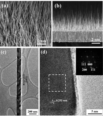
A large area and quasi-aligned tungsten nanowire array was successfully synthesized under a
pressure of 13∼15 Torr with an air flow of 200 sccm at a temperature of 1000◦C. Figure 2.1 shows typical FESEM images of an as-synthesized nanowire array grown on Si substrate. Nanowires are
distributed evenly with the length of about 3∼5µm as shown in the top view of Figure 2.1(a) and cross-sectional view of Figure 2.1(b), respectively. In fact, the nanowire array grows out from a
thin layer of tungsten oxide nanoparticles formed prior to the nanowire growth shown in the insert
of the enlarged interface in Figure 2.1(b).
Figure 2.1: SEM images of a WO3nanowire array grown on a Si substrate from a top view (a) and a cross-sectional view (b). [115]
can be well indexed to a monoclinic WO3 phase with unit cell parameters as a=0.7297 nm,
b=0.7539 nm, c=0.7688 nm, β =90.91◦ (JCPDS 43-1035). In the XRD pattern, the (002)
diffraction peak is the strongest reflection, indicating the (002) is the preferential growth plane
of the nanowires. The strong peak marked by a star in the pattern is from the Si substrate. It is
apparent that the tungsten oxide synthesized in our experiment is WO3 phase, other than W18O49
which was further confirmed by TEM investigation.
Figure 2.5(a) presents a low magnification TEM image of the nanowires with a diameter around
40∼ 50 nm. Figure 2.5(b) is the high resolution electron image (HREM) of the nanowire along
[100]zone from the rectangular area in Figure 2.5(a), in which the lattice spacings are measured to
be 0.385 nm and 0.379 nm along two orthogonal directions, corresponding to the (002) and (020)
planes of monoclinic WO3, respectively. The selected-area electron diffraction pattern (SAED)
proves the nanowire is single crystalline with the growth plane parallel to (002), as shown in the
inset in Figure 2.5(b). Furthermore, EDS analysis shows the atomic ratio of W and O are close to
3:1. The C and Cu peaks are from the copper grid in the EDS spectrum. From the XRD and TEM
analysis, it can be further concluded that the WO3nanowires are single monoclinic crystalline with
Figure 2.2: XRD spectrum of the WO3nanowire array grown on Si substrate. [115]
No catalyst droplets were found on the tips of tungsten oxide nanowires indicating the whole
synthesis process follows the vapor-solid (VS) mechanism [67]. Generally, gas-phase
supersat-uration in VS growth is a most determining factor for the formation of different nanostructures,
which is influenced by source materials temperature, tube pressure, gas flow rate, etc. Therefore,
a series of experiments were performed to investigate the optimum growth conditions. It is found
that relatively low pressure (13∼15 Torr), moderate temperature (1000◦C), and high air flow rate (200 sccm) are able to produce a suitable gas-phase supersaturation for nanowire array growth.
During the heating, the color of the source materials changed from dark gray to orange-reddish,
accompanied with an obvious volume increase. Owing to the sufficient oxygen introduced from
the air flow, WO3species were directly carried down stream, forming WO3nanowire arrays on the
Si substrate. No catalysts were observed at the tips of the nanowires by SEM or TEM. It should be
noted that a layer of WO3nanoparticles, acting as a seed layer, was formed prior to the nanowire
Figure 2.3: (a) A typical low magnification TEM image of tungsten oxide nanowires. (b) [100]
HREM image of a tungsten oxide nanowire denoted by the white rectangle in (a). The inset shows the corresponding SAED pattern. The white arrow in (a) indicates the growth direction of the nanowire. (c) EDS spectra of the as-prepared nanowires reveal that nanowires consist of W and O. The C and Cu elements are from the TEM copper grids. [115]
2.1.3
Sensing Performance of Gas Sensors Based on Monoclinic
WO
3Nano-wire Arrays
The nanowire array gas sensor was prepared by a multiple-step photolithography process [116]
test-Figure 2.4: Schematics and SEM images showing the procedures to prepare a gas sensor based on WO3nanowire array. All the scale bars are 4µm. [115]
ing cell for sensor measurements. The gas testing experiments of the sensor under air-diluted NO2
were conducted at 180◦C using a Keithley 2400 source meter. A gas sensor was prepared based on
this WO3nanowire array and the schematic diagram and corresponding SEM images of the
prepa-ration process are shown in the Figure 2.4. A layer of 8 µm polymethyl methacrylate (PMMA)
Resist (950A4, Microchem Inc.) was first coated on the nanowire array by spin coating, shown in
Figure 2.4(b). After the heat treatment on the PMMA resist, the nanowire array was loaded to an
oxygen plasma etching machine (SPI Plasma Prep II). A 100 W input power resulted in an etch
Figure 2.5: (a) I-V curves of gas sensors based on the WO3 nanowire array being exposed to air-diluted NO2with different concentrations. (b) Sensing response curves of the sensor. [115]
nanowires were exposed to the environment [Figure 2.4(c)]. By using sputtering and a metal mask,
a 100 nm gold layer with 2 mm×2 mm area was coated onto the residue PMMA and connected to the tips of the nanowires. After that, the nanowire array was soaked into acetone, isopropyl
alcohol, and deionized water, successively, to remove the PMMA. Finally, the sensor was dried
by slow nitrogen flow. Silver paste was used to make connections from the testing system to the
bottom layer and the top gold electrode [Figure 2.4(d)]. By applying a voltage on the top electrode,
current flowing through the nanowires could be provided and all of the nanowires were exposed to
the atmosphere.
The sensor was first stabilized at 180◦C in pure air.I-V curves were obtained when air-diluted
NO2 with different concentrations were introduced into the gas sensor testing cell, as shown in
Figure 2.5(a). All the I-V curves are linear, implying ohmic contacts were formed between the
deposited Au and WO3. The sensor can detect NO2with a concentration down to 50 ppb. When
the sensor is exposed to 50 ppb NO2, the resistance of the sensor increased to about 37% from
45.5 MΩto 62.5 MΩ. Even at a relatively low concentration, 5 ppm, the resistance change can
be as high as 3400% from 45.5 MΩto 1.6 GΩ. The sensing response curves to air-diluted NO2
times are less than 30 s; however, it took a relatively long time for the sensor recovery, generally
more than 800 s, and it increased as the exposed concentration increased. The response curves
for the low concentrations are also plotted in the inset of Figure 2.5(b), which indicates that the
response signal was much larger than the background noise level, even at a concentration as low
as 50 ppb and can be easily identified. Therefore, the sensor presents high sensitivity to detect
NO2gases, which might be attributed to the large surface area of the nanowire array and intrinsic
properties of the monoclinic WO3nanowires.
WO3 is ann-type semiconductor. Adsorbing oxidizing gas molecules, such as O2 and NO2,
to its surface, can induce surface states that trap electrons and result in depletion of carrier on the
material surface. For nanowires, forming a carrier depletion layer will reduce the effective cross
area for carrier transport and cause reduced current in our constant voltage bias measurement.
Considering that the nanowires are resistors with parallel connection, overall resistance increase
in our device requires the gas to cause resistance increase in most of the nanowires. Since the
response speed of this sensor is very fast, gas diffusion into the nanowire array sensor must be very
effective so that it can induce a resistance increase in most nanowires in a short time. Though the
response trend is the same as other WO3based sensors [109, 117], the unique parallel connection
with large surface area provides a new route to fabricate highly sensitive gas sensors.
2.1.4
Summary
In summary, a large area WO3nanowire array with diameters ranging from 40 to 100 nm and
lengths up to 5µm was synthesized on Si substrate using a convenient thermal evaporation method
at a relatively low temperature. The nanowire grew on top of WO3nanoparticle seed layers,
form-ing a quasi-aligned nanowire array. The nanowires were sform-ingle crystalline with monoclinic
struc-ture. The nanowire array gas sensors were also fabricated using a multiple step photolithography
method. Gas sensing tests revealed that the sensor based on the WO3nanowire array had the