Please cite this article as: M. Asemani, G. Ardeshir, D. Razmjooei, Improving Linearity of CMOS Variable-gain Amplifier Using Third-order Intermodulation Cancellation Mechanism and Intermodulation Distortion Sinking Techniques, International Journal of Engineering (IJE), TRANSACTIONS B: Applications Vol. 30, No. 2, (February 2017) 192-198
International Journal of Engineering
J o u r n a l H o m e p a g e : w w w . i j e . i r
Improving Linearity of CMOS Variable-gain Amplifier Using Third-order
Intermodulation Cancellation Mechanism and Intermodulation Distortion Sinking
Techniques
M. Asemani*a, G. Ardeshira, D. Razmjooeib
a Department of Electrical and Computer Engineering, Babol University of Technology, Babol, Iran
b Department of Communications and Electronics, School of Electrical and Computer Engineering, Shiraz University, Shiraz, Iran
P A P E R I N F O
Paper history: Received 31 August 2016
Received in revised form 27 January 2017 Accepted 30 January 2017
Keywords:
Variable-gain Amplifier Distortion Cancellation Linearity Improvement Third-order Input Intercept Point
A B S T R A C T
This paper presents an improved linearity variable-gain amplifier (VGA) in 0.18-µm CMOS technology. The linearity improvement is resulted from employing a new combinational technique, which utilizes third-order-intermodulation (IM3) cancellation mechanism using second-order-intermodulation (IM2) injection, and second-order-intermodulation distortion (IMD) sinking techniques. The proposed VGA gain cell consists of a variable-gain attenuator followed by a differential cascode amplifier as a fixed-gain stage. The continuous gain control mechanism in the first stage occurs by varying the gate voltage of an nMOS transistor. Our proposed linearization technique is applied to the fixed gain cascode amplifier of the second stage. To examine the linearity of the proposed circuit, a nonlinear analysis of the cascode amplifier based on Taylor series has been performed. The simulation results show that after linearization, the third-order input intercept point (IIP3) of the whole VGA has
been improved about +18 dB at the gain of 15.4 dB. The VGA has a voltage gain varying from -7.5 to 19.5 dB and a bandwidth of 830 MHz to 845 MHz. Morever, the circuit dissipates 4.65 mW to 9.35 mW from a 1.8 V single supply over the entire gain range.
doi: 10.5829/idosi.ije.2017.30.02b.05
1. INTRODUCTION1
Variable-gain amplifier (VGA) is an essential sub-system in receivers which maximizes the whole dyna-mic range and is used in many applications such as disk drives [1] and wireless communication links [2]. In a modern communication receiver, a VGA usually pre-ceds an analog-to-digital converter (ADC) to adapt the loss variation of the transmission channel and in turn ease the dynamic range requirement of the ADC [2].
A VGA must keep two main characteristics simult-aneously; a controllable gain and a good linearity. However, many of recently reported VGAs have poor linearity. In a high-speed programmable gain amplifier (PGA) designed using variable MOS transconductors in disk drive applications, the linearity is limited by
1*Corresponding Author’s Email: [email protected] (M. Asemani)
near characteristics of the transconductors [1, 3]. One of the main challenges of a gm-ratioed VGA which its gain
is controlled by the gm ratio of the input to load stages,
comes from the load stage distortion which significantly affects output linearity over the entire gain range [4, 5]. The linearization in resistive source degeneration techn-ique improves the system linearity, however, increases noise and power dissipation [6]. Also, VGAs with poor linearity can be seen in other works [7-9].
Using cascode amplifier topology in VGAs, due to its advantageous properties over the common-source amplifier, results better high-frequency operation and wider dynamic range [10-13]. Elwan et al. [14] have used a cascode structure in a VGA and reported its superiorities over common-source amplifier but the linearity is still unpleasant.
larger voltage-gain and a much better linearity. The proposed VGA consists of a variable-gain attenuator followed by a fixed gain cascode amplifier. The gain variation mechanism is realized via controlling the gate bias voltage of the nMOS transistor in the first stage. In order to improve the VGA’s linearity, we have combi-ned two techniques simultaneously: one is injecting an IM2 signal to the common-source node [16] of the cascode amplifier and second is sinking the same ampli-fier’s output current [17]. By tuning some parameters, our novel technique has significantly lowered the IM3 component of the output current which leads to increa-sing the IIP3 of the whole VGA. Furthermore, to
exam-ine the performance of the circuit, a nonlexam-inear analysis based on Taylor series has been conducted on the cascode amplifier. Simulations verify excellent linearity improvement and larger gain dynamic range. Because of the superior linearity, the proposed VGA best suits the applications requiring high linearity such as direct conversion receiver (DCR). The rest of the paper is organized as follows. Section 2, provides the proposed linearized VGA (L-VGA) design and analysis. Section 3, shows the simulation results and finally, conclusions are presented in Section 4.
2. PROPOSED LINEARIZED VGA DESIGN AND ANALYSIS
This section presents the proposed linearized VGA structure consisted of an attenuator stage followed by a fixed-gain stage, separately. Then, to investigate how the cancellation mechanism works, a nonlinear analysis of the circuit based on Taylor series theory is introduced.
2. 1. Attenuator Stage Circuit Design Figure 1
depicts the variable gain attenuator structure of the first stage. The attenuator topology is a source follower (M1, M2) with active load nMOS (M3, M4) biased in triode region. Simply, from the small signal low-frequency model of a source follower (neglecting body effect), the voltage gain of the circuit is given by [18]:
( )1, 2 - ( )
1 1 1
( )1, 2 - ( )
1, 2 3, 4
W
C V V V
n ox L cont o Th G
W
C V V V
n ox L cont o Th r r
o o
(1)
+
v
o-v
in+Vcont-v
in+Vcont VDDVbt
M1 M2
M3 M4
Figure 1. Schematic of the attenuator stage as a variable-gain cell
Equation (1) shows that the voltage gain of the atten-uator can be varied by the control voltage Vcont.
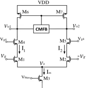
2. 2. Fixed-gain Stage Circuit Design Figure 2
shows the fixed-gain differential cascode amplifier of the second stage. M1 and M2 are the input transcondu-ctor and M4 and M5 are the common-gate stages. M6 and M7 are pMOS active load current sources and M3 acts as the tail current source. In order to set a proper common-mode output voltage VCM, a DC level sensing pair along with a common-mode feedback (CMFB) circuit is used.
Considering the input-stage differential pair of the cascode amplifier shown in Figure 2, the time-varying drain current I1 can be expressed as a function of the
small-signal gate-source voltage (vgs) around its bias
point, appropriately chosen on the I-V charecteristics of device M1, using Taylor series expansion as:
1 1 1 1
2 3
' '' ...
d g s g s g s
i g v v g v v g v v (2)
where g1, g1' and g1" are the jth-order, (j = 1,2,3),
transcenductance coefficients of input device respecti-vely, given by [16]:
The third-order term in Equation (2) is the main contribution of IM3 components in the transconductor -stage. However, the multiplying term -2g'mvgvs in g'm (vg
-vs) also contributes to IM3 because vs contains intrinsic
IM2 components [16]. Therefore, the linearization of the
cascode amplifier is a significant consideration.
2. 3. Distortion Analysis of the VGA Topology
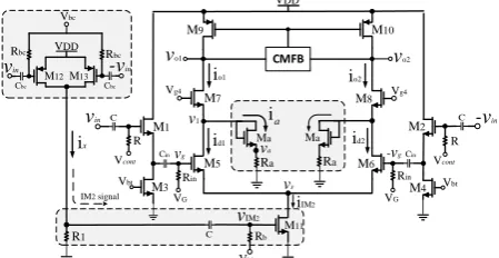
W-ith the Proposed LinearizationTechnique The
complete linearized VGA structure is shown in Figure 3. The IM2 generator composed of M12 and M13, generates the IM2 current (ix) which is then converted to
the IM2 voltage (vIM2) through resistor R1. Here, M3
converts vIM2 to the current iIM2 and inject it to the vs
node.
1
I I2
CMFB
Vg4 Vg4
Vbias
M1 M2
M5
M4
M6 M7
v
o1v
o2VDD
v
sv
g-v
gM3
Iss
An AC coupling network, formed by C and Rb, is
inserted between the bias transistor and the squaring circuit to facilitate the DC bias of M3. The iIM2, id1 and
id2 come together which results in lower output IM3
cpmponents [16].
For further suppression of the output IM3 compo-nent in current io, we have used an additional
diode-connected nMOS transistor Ma (as ia injected into the v1
node in Figure 3), as an IMD sinker [17].
Here, the source follower of the first stage is considered to be linear because of its low intermodulation distortion [19]. Thus, our analysis is focused on the cascode amplifier of Figure 3.
At the beginning, we define iIM2 as 2X×vin2 and vg =
G1.vin . The relation between differential output current
io and input voltage vin, in Figure 3, is a nonlinear
differential equation which can be described as a Taylor series expansion as below:
3 5
1. 3 in 5 in ...
ioC vinC
v
Cv
(4)Differential circuits exhibit an odd-symmetric input/o-output characteristic [9]. It indicates that a differential circuit driven by a differential signal produces no even-order harmonics as expressed in Equation (4). In the equation above, C1 is the first-order term of the output
current that refers to the small signal gain. C3 and C5 are
the third and fifth-order nonlinearity coefficients, resp-ectively. For analyzing IM3 and IIP3, our analysis is
focused on C3. Thus, the above polynominal is limited
to the third-order term. By solving KCL equations (neglecting second order effects), the expression for id1
is obtained as below [16]:
1 1 1 1 1 1 1 1 2 3 1 1 1 1 2 '
2 2 3 3
'
' ''
1 ( ) in ( ) in ( 2 ) 2 in
d G G X G XG
A A A g g g g
i g v g v g v
(5)
In Equation (5), A1 is the small signal gain of the
transconductor stage and A2, A3 are the nonlinear
comp-onents in id1. The first terms in A2 and A3 are the
intrinsic nonlinearities and the second ones are introd-uced by the new linearization technique.
ia
C IM2 signal
CMFB C C M8 M10 M9 M7
M1 M2
M4 M3
VG VG
Vbt
Vcont vg -vg Vcont
v1
M5 M6
id1 id2
io1 io2
vo1 vo2
Vg4 Vg4
VDD
VDD
R1 Rb
Vbias
-vin
vin
ix M12M13
vin -vin
Rbc Rbc
Vbc
M11 vs
Rin Rin
Cin
Ra Ra
va Ma Ma
iIM2
Cin
vIM2
Vbt
R R
Cbc
Cbc
Figure 3. Circuit schematic of the proposed linearizaed VGA
1 1 1
2 3 2 1 1 ' '' , , 3 2! 3!
DS DS DS
GS GS GS
I I I
V V V
g g g
(3)
To find ia, we first approximate va with respect to v1
with Taylor series expansion as follows [20]:
2 3
1 1
1 1 2 3
a a a a
v g v g v g v (6)
Therefore, ia is obtained through va / Ra:
2 3
1 2 3
1 1
1
a a a a
a
a a a a
g g g
R R R R
v
i v v v (7)
To have ia as a function ofvin, we write v1 = Z1×id1 in
which, Z1 is the equivalent resistance of parallel paths
diode-connection and common-gate. So, ia would be
given as:
2
1 2 1
1
1 1
2 2 1 3 3
1 2 2 1 1 2 1 2 3 3 1
1 2 3
3
1 1
+ 2
in i
a a a
a a n i a a a a a n a a a
g g g
R R R
g g g
R R R
i ZA v Z A Z A v
A A
Z ZA Z A v
(8)
As known, the sum of ia and id1 would be io1 as follows:
2 3
1 1 ( 1 1) in ( 2 2) in ( 3 3) in
o d a
i i i A v A v A v (9)
io2would be the same as io1 if vin is replaced by -vin. The
injected IM2 current from M3, iIM2, is found by [16]:
2 2
2 12 3 1
'
2 in 2 in
IM X m R
i
v
g gv
(10)From io = io1- io2 and Equation (4), C1 and C3 can be
concluded (on the next page).
From Equations (11.a) and (11.b), the third-order input intercept point for the nonlinear output current can be expressed as below [21]:
3
1 (dBm) 10
3
4
IIP 10 log 10 dB
3 C C (12)
An interesting observation on Equation (12) is that by setting C3 to zero the linearity of the VGA can be
maximized. In Equation (11.b), it is observed that the proposed linearization technique has introduced the degrees of freedom which is able to cancel the third- order distortion terms. Therefore, it is apparent from Equation (11.b) that an appropriate choice of resistor and transistor sizes, leads to a lower C3 and results a
better IIP3.
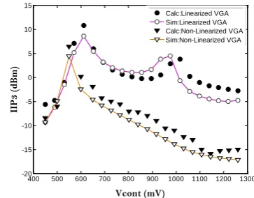
In order to predict the IIP3 behavior, the theoretical
values for IIP3 as a function of tunable parameters such
as resistors R1 and Ra calculated by Equation (12) have
Figure 4. IIP3 variations computed with Taylor series vs. Vcont
and R1
Figure 4(a) illustrates the IIP3 behavior of the VGA
as a function of control voltage and resistorR1 for Ra =
0Ω. For different control voltages, The IIP3 experiences
its maximum values as R1 increases. So, we choose R1 =
4 KΩ as an optimal value.
The IIP3 behavior of the VGA for R1 = 4 KΩ as a
function of control voltage and resistor Ra is shown in
Figure 4(b). As Ra increases, the IIP3 also increases at
control voltages ranging from 600 to 900 mV, but it decreases at high gain modes (Vcont > 900mV). Here, we choose Ra = 200Ω as an optimal value by
considering the low gain linearity importance and also drastic drop at high gain mode.
The theoretical values were obtained for a 100µm/0.18 µm aspect ratio for M4 and M5, 60µm/0.18 µm for M1 and M2 ,and 15µm/0.18 µm for the tail current source M3. The transistor sizing for the squaring circuit (or IM2 generator circuit) is chosen to be 9µm/0.18 µm. Finally, the size of Ma is considered to be 24µm/0.18µm.
3. SIMULATION RESULTS
Simulations using Advanced Design System (ADS) simulator was performed to validate the results of the Taylor analysis in Figure 4. The fully differential variable-gain amplifier, shown in Figure 3, has been simulated using 0.18µm CMOS TSMC model. The cascode biasing current wassetto 1.94 mA, whereas the total current driven from the attenuator stage varied from 49 µA to 2.66 mA. The bias voltage for the squaring circuit, Vbc, and gate voltage of M1 and M2,
Vgate, wasset to 935 mV and 900 mV, respectively. The
total current consumed by the squaring circuit is 456 µA. The IIP3 variation as a function of control voltage
considering the optimal values obtained from the theoretical calculations is illustrated in Figure 5.
The results were plotted before and after applying the linearization technique. As shown in Figure 5, before the linearization technique, the IIP3 reaches its
maximum value at the gain of 2.9 dB then decreases as control voltage increases.
Figure 5. IIP3 variations computed with Taylor series vs. Vcont
andRa
In this case, the minimum and maximum values obtained for the IIP3 are -17.2 dBm and 4.4 dBm, respectively. The linearity of the VGA has improved using the proposed linearization technique as the IIP3
curve shows one more peak at the gain of 14 dB, as shown in Figure 5. The second peak, produced by the linearizer circuit, prevents the IIP3 to decrease as fast as
non-linearized VGA (NL-VGA) does. Therefore, it can be observed from Figure 5 that the new cancellation technique works so good leading to a significant IIP3
improvement of +18 dB at the gain of 15.4 dB. Thus, the minimum and maximum values obtained for the IIP3
is - 9.3 dBm and 8.5 dBm, respectively. As can be seen from Figure 5, by applying the proposed technique,
1 1 2 1 1 1 1 a
a g
C G Z
R
g g
(11 a)
1 12 3 1 1
1 1
1 1 1 1 1 1
1 1 1
3 1
2 3
1 1 1 12 3 1 1 1 1 '
'2 '2 2
'' 2 2 '' 2 2 1
2
2 ' 2 ' 3 3 2
2 1
a m a
a a
a a
m
a a
g g g R g
g g
G Z G Z
g R g g R
C G
g g
Z g g G g g R Z g G
R R
g g
(11 b)
the results have been plotted before and after applying the linearization technique. As shown in Figure 6, before the linearization technique, the IIP3 reaches its
maximum value at the gain of 2.9 dB then decreases as control voltage increases.
Figure 6. Comparison of calculated and simulated IIP3 before and after applying the linearization technique versus control voltage
400 500 600 700 800 900 1000 1100 1200 1300
-20 -15 -10 -5 0 5 10 15
Vcont (mV)
II
P
3
(d
B
m
)
In this case, the minimum and maximum values obtained for the IIP3 are -17.2 dBm and 4.4 dBm, respectively. The linearity of the VGA has improved using the proposed linearization technique as the IIP3
curve shows one more peak at the gain of 15.4 dB, as shown in Figure 5. The second peak, produced by the linearizer circuit, prevents the IIP3 to decrease as fast as
non-linearized VGA (NL-VGA) does. Therefore, it is obvious from Figure 5 that the new cancellation technique worked so good leading to a significant IIP3
improvement of +18 dB at the gain of 15.4 dB. Thus, the minimum and maximum values obtained for the IIP3
is - 9.3 dBm and 8.5 dBm, respectively. As can be seen from Figure 5, by applying the proposed technique, input linearity of the VGA has improved very well and a good agreement with Figure 4(b) is also evident.
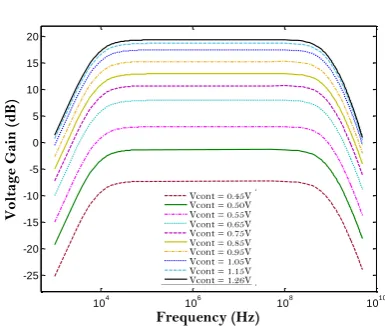
Figure 7 shows the frequency response obtained from the simulation with control voltage ranging from 0.45 V to 1.26 V. The upper 3-dB bandwidth is 830 MHz and 845 MHz at high gain and low gain modes, respectively. A high-pass filter with a low cut off frequency would be enough to block the DC offsets from preceding stages and provide a correct bias for the cascode stage. As it can be seen from Figure 6, there is a BW variations of about 15 MHz over the entire gain range.
Figure 8 illustrates the VGA voltage gain over different control voltages obtained from the simulation. By applying the linearization technique, the gain of the VGA does not change at all, therefore the dynamic range remains constant. The VGA achieves a gain range from -7.5 to 19.5 dB.
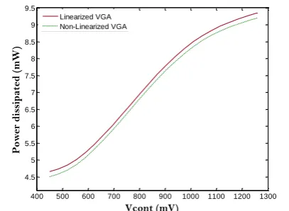
Figure 9 illustrates the total power dissipation of the VGA for different gain control voltages. The power dissipation of the linearized and non-linearized VGA are shown with solid and dashed lines, respectively. As it can be seen from Figure 8, there is a slight difference between these two curves which is about 0.15 mW.
To compare the VGA’s efficiency before and after linearization, a figure of merit (FoM) based on linearity,
bandwidth, voltage gain, noise and power consumption is defined as:
3( ) ( )
( ) ( 1) 1( )
dc
IIP mW gain BW MHz
FOM
P mW F MHz
(13)
where, F is the noise factor of the VGA.
Figure 7. Simulated frequency response vs. various control voltages
Figure 8. Simulated voltage gain over control voltage
TABLE 1. Performance summary and comparison
REF. 2009 [14] 2013 [15] 2011 [7] 2012 [8] 2013 [9] 2012 [5] This work: NL-VGA
This work:
L-VGA Units
Process 65 90 180 180 180 180 180 180 nm
IIP3 -25* -19~3 -4.5~0 -18* -1.4~ -2.9# N/A -17.2~4.4 -9.3~8.5 dBm
BW 40 56~64** 1000~5000 0~5600 2~1900 76~809 850~865 830~845 MHz
Gain -18~47 -18~22 -5~11 -16.5~6.5 -10.6~7.8 -37~28 -7.5~19.5 -7.5~19.5 dB
NF N/A 4.8~18 3.2~7.2 16.5~27.1 21.4~27.1 22 13~16 13~16 dB
Power 2.23 26 10~19 7.9 12.2 3.1~5 4.5~9.2 4.65~9.35 mW
Supply 1.2 2 1.8 1.8 1.8 1.8 1.8 1.8 V
FOMmax N/A N/A N/A N/A N/A N/A 1.1^ 85^
* Reported values are for the maximum gain setting. # Estimated from the input P1dB.
^ Values were calculated at 15.4 dB where the FOM is maximum. ** Reported value is in GHz.
104 106 108 1010
-25 -20 -15 -10 -5 0 5 10 15 20
Frequency (Hz)
V
o
lt
ag
e
Ga
in
(d
B
)
Vcont = 0.45V Vcont = 0.50V Vcont = 0.55V Vcont = 0.65V Vcont = 0.75V Vcont = 0.85V Vcont = 0.95V Vcont = 1.05V Vcont = 1.15V Vcont = 1.26V
400 500 600 700 800 900 1000 1100 1200 1300
-5 0 5 10 15 20
Vcont (mV)
V
o
lt
ag
e
Ga
in
(d
B
)
Figure 9. Total power dissipation across different control voltages
4. CONCLUSION
This paper developed a variable-gain amplifier with low IM3 components resulted from injecting low frequency IM2 and using the diode-connection transistors for sinking nonlinear components of output current. The proposed VGA was analyzed by Taylor series. Simulation results in 0.18µm TSMC CMOS technology demonstrated a maximum IIP3 improvement of +18 dB
at the gain of 15.4 dB. The excess power consumption is about 0.15 mW. The obtained bandwidth varies 15 MHz (830MHz to 845MHz) in the whole gain range. The achieved noise figure (NF) of the linearized VGA is between 13 to 16 dB at the entire gain range.
5. REFERENCES
1. Harjani, R., "A low-power cmos vga for 50 Mb/s disk drive read channels", IEEE Transactions on Circuits and Systems II:
Analog and Digital Signal Processing, Vol. 42, No. 6, (1995),
370-376.
2. Jeon, O., Fox, R.M. and Myers, B.A., "Analog AGC circuitry for a CMOS WLAN receiver", IEEE Journal of Solid-State
Circuits, Vol. 41, No. 10, (2006), 2291-2300.
3. Gomez, R. and Abidi, A., "A 50-MHz CMOS variable gain amplifier for magnetic data storage systems", IEEE Journal of
Solid-State Circuits, Vol. 27, No. 6, (1992), 935-939.
4. Duong, Q.-H., Le, Q., Kim, C.-W. and Lee, S.-G., "A 95-dB linear low-power variable gain amplifier", IEEE Transactions on Circuits and Systems I: Regular Papers, Vol. 53, No. 8, (2006), 1648-1657.
5. Chen, Z., Zheng, Y., Choong, F.C. and Je, M., "A low-power variable-gain amplifier with improved linearity: Analysis and
design", IEEE Transactions on Circuits and Systems I:
Regular Papers, Vol. 59, No. 10, (2012), 2176-2185.
6. Mollaalipour, M. and Miar-Naimi, H., "An improved high linearity active cmos mixer: Design and volterra series analysis",
IEEE Transactions on Circuits and Systems I: Regular
Papers, Vol. 60, No. 8, (2013), 2092-2103.
7. El-Gabaly, A. and Saavedra, C., "Wideband variable gain amplifier with noise cancellation", Electronics letters, Vol. 47, No. 2, (2011), 116-118.
8. Kumar, T.B., Ma, K. and Yeo, K.S., "A 7.9-mW 5.6-GHz digitally controlled variable gain amplifier with linearization",
IEEE Transactions on Microwave Theory and Techniques,
Vol. 60, No. 11, (2012), 3482-3490.
9. Kumar, T.B., Ma, K. and Yeo, K.S., "Temperature-compensated db-linear digitally controlled variable gain amplifier with DC offset cancellation", IEEE Transactions on Microwave Theory
and Techniques, Vol. 61, No. 7, (2013), 2648-2661.
10. Kwon, J., Kim, K., Song, W. and Cho, G., "Wideband high dynamic range CMOS variable gain amplifier for low voltage and low power wireless applications", Electronics letters, Vol. 39, No. 10, (2003), 759-760.
11. Lee, H.D., Lee, K.A. and Hong, S., "A wideband cmos variable gain amplifier with an exponential gain control", IEEE
Transactions on Microwave Theory and Techniques, Vol. 55,
No. 6, (2007), 1363-1373.
12. Razavi, B. “Design of analog CMOS integrated circuits”, New York, McGraw-Hill, (2001).
13. Lee, T.H., "The design of CMOS radio-frequency integrated circuits, Cambridge university press, (2003).
14. Elwan, H., Tekin, A. and Pedrotti, K., "A differential-ramp based 65 dB-linear vga technique in 65 nm cmos", IEEE Journal of Solid-State Circuits, Vol. 44, No. 9, (2009), 2503-2514.
15. Yeh, H.-C., Aloui, S., Chiong, C.-C. and Wang, H., "A wide gain control range V-Band CMOS variable-gain amplifier with built-in linearizer", IEEE Transactions on Microwave Theory
and Techniques, Vol. 61, No. 2, (2013), 902-913.
16. Lou, S. and Luong, H.C., "A linearization technique for RF receiver front-end using second-order-intermodulation injection", IEEE Journal of Solid-State Circuits, Vol. 43, No. 11, (2008), 2404-2412.
17. Zhang, H., Fan, X. and Sinencio, E.S., "A low-power, linearized, ultra-wideband LNA design technique", IEEE Journal of Solid-State Circuits, Vol. 44, No. 2, (2009), 320-330.
18. Shedge, M.D., Itole, M.D., Gajare, M.M. and Wani, P., "Analysis and design of CMOS source followers and super source follower", ACEEE International Journal on Control
System and Instrumentation, Vol. 4, No., (2013).
19. Fan, X. and Chan, P.K., "Analysis and design of low-distortion CMOS source followers", IEEE Transactions on Circuits and
Systems I: Regular Papers, Vol. 52, No. 8, (2005), 1489-1501.
20. Chang, C.-P., Chien, W.-C., Su, C.-C., Wang, Y.-H. and Chen, J.-H., "Linearity improvement of cascode CMOS lna using a diode connected nmos transistor with a parallel RC circuit",
Progress In Electromagnetics Research C, Vol. 17, (2010),
29-38.
21. Razavi, B. and Behzad, R., "Rf microelectronics, Prentice Hall New Jersey, Vol. 2, (1998).
400 500 600 700 800 900 1000 1100 1200 1300
4.5 5 5.5 6 6.5 7 7.5 8 8.5 9 9.5
Vcont (mV)
P
o
w
er
d
is
si
p
at
ed
(m
W
)
Improving Linearity of CMOS Variable-gain Amplifier Using Third-order
Intermodulation Cancellation Mechanism and Intermodulation Distortion Sinking
Techniques
M. Asemania, G. Ardeshira, D. Razmjooeib
a Department of Electrical and Computer Engineering, Babol University of Technology, Babol, Iran
bDepartment of Communications and Electronics, School of Electrical and Computer Engineering, Shiraz University, Shiraz, Iran
P A P E R I N F O
Paper history: Received 31 August 2016
Received in revised form 27 January 2017 Accepted 30 January 2017
Keywords:
Variable-gain Amplifier Distortion Cancellation Linearity Improvement Third-order Input Intercept Point
ديكچ ه
هدننک تیوقت کی هلاقم نیا رد رد هتفای دوبهب یناسطخ اب ریغتم هرهب ی
یروانف CMOS 18 / 0 دوبهب .تسا هدش هئارا رتمورکیم
کی هئارا اب یناسطخ هویش
هفلوم بذج و مود هبترم یلخاد نویسلاودم هفلوم قیرزت لماش دیدج یبیکرت نویسلاودم یاه
هقبط کی و ریغتم هرهب اب ژاتلو هدننک فیعضت هقبط کی زا لکشتم هدننک تیوقت نیا رد هرهب لولس .تسا هتفرگ ماجنا یلخاد
.دشاب یم تباث هرهب اب یلضافت دوکسک هدننک تیوقت راکوزاس
تیگ ژاتلو رییغت اب هدننک فیعضت هقبط رد هرهب هتسویپ لرتنک
روتسیزنارت n یم تروص یدورو لاناک ،هلاقم نیا رد .دریذپ
هویش یطخ تیوقت هب رادم یناسطخ دوبهب تهج یداهنشیپ یزاس
و یناسطخ یسررب تهج .تسا هدش لامعا مود هقبط دوکسک هدننک نومزآ
رب یطخریغ لیلحت کی ،یداهنشیپ رادم درکلمع
ح جیاتن .تسا هتفرگ ماجنا دوکسک هقبط یور رب رولیت یرس ساسا یم ناشن حرط نیا یزاس هیبش زا لصا
لامعا زا سپ هک دهد
هویش هدننک تیوقت یدورو رد موس هبترم دروخرب هطقن ،رادم هب یداهنشیپ نازیم هب ریغتم هرهب ی
18 ژاتلو هرهب رد لبیسد 4
/ 15
زا هدننک تیوقت ژاتلو هرهب .تسا هتفای دوبهب لبیسد 5
/ 7 ات 5 / 19 دناب یانهپ اب لبیسد 830
ات 845 .تسا هدمآ تسدب زترهاگم
دودح رد رادم لک یفرصم ناوت ،نینچمه 4.5
ات 9.35 هیذغت عبنم زا تاو یلیم 8
/ 1 .دشاب یم یتلو