1
Bendable ZnO thin film surface acoustic wave devices on polyethylene
terephthalate
substrate
Xingli He,1 Hongwei Guo,1 Jinkai Chen, Wenbo Wang,1 Weipeng Xuan,1 Yang Xu1,a) and Jikui Luo1,2,a)
1
Dept of Info. Sci. & Electron. Eng., Zhejiang University and Cyrus Tang Center for Sensor Mater. &
Appl., 38 Zheda Road, Hangzhou 310027, P.R. China.
2
Inst. of Renew. Energ. & Environ. Tech., University of Bolton, Deane Road, Bolton,BL3 5AB, United
Kingdom.
Abstract: Bendable surface acoustic wave (SAW) devices were fabricated using high quality
c-axis orientation ZnO films deposited on flexible polyethylene terephthalate (PET)
substrates at a low temperature of 120 ℃. Dual resonance modes, namely, the zero order
pseudo asymmetric (A0) and symmetric (S0) Lamb wave modes, have been obtained from the
SAW devices. The SAW devices are very flexible and durable, and perform well even after
being bent with a large strain of 2500 με up to 100 times, demonstrated its suitability for the
application in flexible electronics. The SAW devices were also found highly sensitive to
compressive and tensile forces, exhibiting excellent anti-strain deterioration property, thus
they are particularly suitable for the application in sensing large strains.
Keywords: Bendable, SAW, ZnO, PET, Strain
2
Motivated by the fundamental advancement of material science and the progress of
the-state-of-the-art fabrication technology, flexible/stretchable electronics have progressed
rapidly in recent years. Flexible/stretchable electronics are not just as a supplement to the
established rigid substrate-based electronics, but also a vital and innovative branch which
opens the door for variety of new applications. Many applications of flexible electronics have
been reported, such as hemispherical eye-type camera1,2, graphene-based flexible transistors,3
stretchable nanogenerators4,5, bendable supercapacitor6, to name a few.
The stretchable microelectromechanical systems (MEMS) are an important part of
flexible electronic devices. Various flexible MEMS devices have been developed, e.g. the
flexible film bulk acoustic wave resonators7, micromachined infrared bolometers,8 and
piezoelectric pressure sensors9 etc. Surface acoustic wave (SAW) devices are an important
member of MEMS family, as they have been widely used as filters and frequency regulators
in communication, and as micro-sensors10 as well as microfluidic devices.11 However,
conventional SAW devices are made on rigid substrates such as LiNbO3, LiTaO3, Quartz etc.
Polymers such as polydimethylsiloxane (PDMS)1,2, polyimide (PI)7,polyethylene naphthalate
(PEN)12, polyethersulfone (PES)13 and polyethylene terephthalate (PET) 6,9 etc, are
commonly used to achieve the flexibility and bendability for electronics. Recently we have
successfully developed flexible SAW devices on PI substrates, and demonstrated its
application in electronics, sensors and microfluidics14. PI substrates are flexible, but with
relatively poor anti-strain property, which would make the ZnO film deposited on it fragile
and easy to crack when bent and stretched. Here we report a ZnO film based bendable SAW
device using PET as the flexible substrate, and demonstrate the performance of the SAW
devices under various strains, and explore its application as a strain sensor.
Due to the excellent properties such as flexibility, high transparency, thermal and
chemical stability, as well as low cost, PET has been widely used as the substrates for flexible
electronics and optoelectronics, with one most popular application as the mobile phone
screen protector. In this work, 125 μm thick commercial PET films used as mobile phone
3
aim for the development of SAW passive wireless sensors on mobile phones.
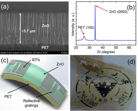
FIG. 1. A SEM picture of the cross-sectional morphology of a 3.7 μm thick ZnO film on its PET substrate (a),
the XRD pattern of the ZnO layer (b), a 3D schematic of the flexible SAW on the ZnO/PET (c) and a
photograph of bendable transparent SAW devices fabricated on the PET (d).
Highly (0002) crystal orientation ZnO films were sputtered on the PET films at a low
temperature of 120 ℃, in which the details of the optimized deposition conditions were
summarized in our previously work15. As illustrated by Figs. 1(a) and 1(b), the deposited
ZnO has a large columnar grain structure, perpendicular to the PET surface. The peak at
34.3°in the XRD curve shows the (0002) crystal orientation. The small peak at ~26.1°in
the XRD spectrum corresponds to the (100) orientation of the PET substrate. The typical
thickness of the ZnO film is in the range of 3.5 -4.5 µm.
The conventional ultraviolet light lithography technique was employed to pattern the
interdigitated transducers (IDTs) for the SAW devices. Figure 1(c) shows a schematic
drawing of the device structure, while the real bendable SAW device fabricated is shown in
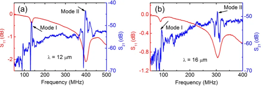
Fig. 1(d). Devices with acoustic wavelengths of λ=12, 16, 20, 24, 28 and 32μm, respectively,
were fabricated on the same ZnO/PET. As shown in Fig. 2, two well-defined resonant wave
modes, termed as mode I and mode II, are observed. For the given ZnO thickness, the
amplitude of the transmission spectrum attenuates with the decrease of the normalized
4
for the device with λ=16 μm, the amplitudes of the dual resonant modes are much weaker
than those of the device with λ=12 μm, indicating the performance of the devices deteriorates
with the increase in wavelength. Although the transmission characteristics of the devices
deteriorate rapidly with the decrease of hk, the influence of thickness on the reflection
characteristics is not significant as shown in Figs. 2(a) and 2(b). Clear and well-defined
resonant peaks can still be obtained from the reflection spectrum of the device with λ=32 μm.
For the same device with a fixed wavelength, the resonant peaks of the transmission spectrum
become much weaker as the film thickness was decreased, implying the thickness of the films
should be carefully designed besides the quality of the piezoelectric films. The length of
acoustic path is another key factor that degrades the transmission severely, which is
especially true for the soft PET substrate as it absorbs acoustic waves16, 17, From the
experimental results of our devices, the transmission characteristics of the devices degraded
obviously when the distance between the two IDTs increases, the acoustic path should better
not exceed 30λ, a smaller distance between the two IDTs, like 20λ or 10λ, can makes the
performance of the devices acceptable.
FIG. 2. Transmission and reflection spectra of the bendable ZnO/PET SAW devices, in which two resonant
modes are obtained. The wavelengths of the devices are 12 μm (a) and 16 μm (b), respectively. The thickness of the ZnO film is 3.7μm. Each device has 50 pairs of IDT fingers and the distance between two IDTs is 20λ.
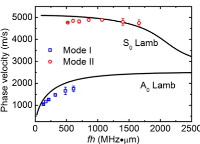
When the thickness of the ZnO film is comparable to the resonant wavelength, Lamb
waves can be obtained. The two resonant peaks are believed to be the zero-order Lamb wave,
5
surface deformations at different frequencies. To confirm our initial speculation, a theoretical
analysis was carried out. Considering the zero order Lamb wave, modeling based on the
transfer matrix method showed that the two layer structure can be simplified as a single
layer18, and the simplified single layer model was used for the analysis here. The velocities of
the Lamb waves are determined by the Rayleigh-Lamb frequency equations as follows19,
2 2 2 2
tan / 2 4
tan / 2 ( )
ts ts tl
tl ts
k h k k
k h k
β β = −
− (1)
2 2 2 2
tan / 2 ( )
tan / 2 4
ts ts
tl ts tl
k h k
k h k k
β β
−
= − (2)
where kts, ktl, h andβ are the shear transverse wave vector, longitudinal transverse vector, film
thickness and propagation factor, respectively. Eq.(1) is related to the symmetric solutions,
while Eq.(2) to the anti-symmetric solutions. The relationships between the transverse wave
vector and propagation factor are expressed as19
2 2 2
( ) ts s k v ω β
= − (3)
2 2 2
( ) tl l k v ω β
= − (4)
where ω is the angle frequency, vl and vsthe longitudinal and shear velocity of the ZnO film,
respectively. The propagation factor β=ω/V, where V is the velocity of the Lamb wave.
Figure 3 shows the comparison between the theoretical and experimental results. The
change of the measured phase velocity for both the modes fits well with the theoretical
analysis, implying that the mode I and mode II peaks are indeed the A0 and S0 Lamb waves,
6
FIG. 3. Phase velocity for the Lamb waves as a function of fh, the product of the resonant frequency f and film
thickness h. The red circles and blue squares are the experimental results for the Mode I and Mode II waves,
while the solid lines are obtained from the theoretical analysis.
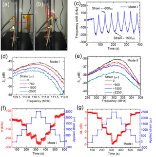
The performances of the ZnO/PET SAW devices under various strains were investigated.
The devices were glued on a flexible steel bar clamped by a movable holder. An automated
mechanical robotic arm (HSV-500) was used to control the movement of the steel bar as
shown in Figs. 4(a) and 4(b). The strain of the device was measured by a strain gauge
(BF1000-3h), which was glued on the back side of the steel bar as well. Figure 4(c) shows the
periodic shift of the resonant frequency of mode I when the device was subjected to repeated
bending. The absolute frequency shift is about 300 kHz when the relative bending strain was
changed from -800 to 1500 με. When the strain is compressive, the resonant frequency of the
device increases. When the strain becomes tensile (the device is under stretching), the
resonant frequency decreases. The shift of resonant frequency under stress is mainly
attributed to the change of the characteristic device wavelength and the acoustic velocity20.
When applying a strain to the device, the surface deformation occurs, which equals to adding
an extra length, Δλ, to the whole wavelength λ. Since the resonant frequency fr=V/(λ+Δλ), the
periodic change of Δλ leads to the shift of the resonant frequency, as represented by Fig. 4(c).
The responses of the resonant frequency and the insertion loss for both the modes to a
stepwise increase of strain are shown in Figs. 4(d)-4(g). When the devices were bent, more
acoustic waves penetrate into the PET layer, leading to the attenuation of the resonances.
Since these devices are bendable and can withstand large strains over 2500 με for many times,
7
applications in flexible electronics. The devices can still work when the strain continues to
increase, most of the devices in our experiments could withstand a large strain over 3500 με,
however, further increasing of the strain will cause cracking of the ZnO films and leads to the
failure of the devices, but when the strain was released (strain = 0με), the devices can still
work. Since they could perform better for large strain sensing applications than conventional
SAW-based strain sensors made on rigid substrates, as most of them could only detect very a
relatively small strain ( ~500 με by Donohoe et al20 and ~1000 by Nomura et al21), therefore
they have great potential for strain sensor application, particularly for sensing large strains.
FIG. 4. Photos of a ZnO/ PET SAW device under test before (a) and after bending at ~40° (b), which
corresponds to an applied strain of ~2500 με. The real time frequency response of the mode I wave under a
stepwise increase of strain with one step duration of t = 46 s (c). Comparison of the transmission spectra of the
devices under different strains up to 2500 με for the mode I (d) and mode II (e) waves. Frequency (f) and
insertion loss (g) response to the stepwise strain change. The wavelength of the device is 16 μm, and the
resonant frequencies for the modes I and II are ~110.7 and ~302.5 MHz, respectively. The thickness of the ZnO
8
In summary, bendable SAW devices were fabricated with high quality ZnO films
deposited on PET substrates. The flexible SAW devices exhibited two resonant wave modes,
the anti-symmetric and symmetric resonances of the Lamb waves, and were confirmed by
theoretical analysis. The performances of the flexible devices under various bending
conditions were investigated, and the sensors worked well even after being bent under a large
strain of 2500 με up to 100 times. Both the two wave modes respond to compressive and
tensile strains with high sensitivity, thus are suitable for strain sensor application.
Acknowledgement: This work was supported by the National Natural Science Foundation of China (No. 61274037 and 61274123), and the Zhejiang Provincial Natural Science Foundation of China (No. Z11101168 and LR12F04001). The authors also would like to acknowledge the financial support by the Innovation Platform of Micro/Nanodevices and Integration System, Zhejiang University.
References
1
Y. Song, Y. Xie, V. Malyarchuk, J. Xiao, I. Jung, K. Choi, Z Liu,H Park, C. Lu, R. Kim, R. Li, K. B. Crozier,
Y. Huang, and J. A. Rogers, Nature 497, 95 (2013).
2
H. Ko, M. Stoykovich, J. Song, V. Malyarchuk, W. Choi, C. Yu, J. B. Geddes, J. Xiao, S. Wang, Y. Huang,
and J. A. Rogers, Nature 454, 748 (2008).
3 C. Sire, F. S. Lepilliet, J. W. Seo, M. C. Hersam, G. Dambrine, H. Happy, and V. Derycke, Nano. Lett. 12,
1184 (2012).
4 K. I. Park, M. Lee, Y. Liu, S. Moon, G. T. Hwang, G. Zhu,J. E. Kim, S. O. Kim, D. K. Kim, Z. L. Wang, and
K. J. Lee, Adv. Mater. 24, 2999 (2012).
5
S. Y. Chung , S. Kim , J.H. Lee , K. Kim , S.W. Kim , C.Y. Kang , S.J. Yoon and Y. S. Kim, Adv. Mater. 24,
6022 (2012).
6
G. Guo, L. Huang, Q. Chang, L. Ji, Y. Liu, Y. Xie, W. Shi, and N. Jia, Appl. Phys.Lett. 99, 083111 (2011).
7
M. Akiyama, Y. Morofuji, T. Kamohara, K. Nishikubo, Y. Ooishi, M. Tsubai, O. Fukuda, and N. Ueno, Adv.
Funct. Mater. 17, 458 (2007).
8 S. Xiao, L. Che, X. Li, and Y. Wang, Microelectron. Eng. 85, 452 (2008).
9 M. Akiyama,Y.Morofuji, T. Kamohara, K. Nishikubo, M. Tsubai, O. Fukuda, and N.Ueno, J. Appl. Phys. 100,
114318 (2006).
10
Y. Q. Fu, J. K. Luo, X. Y. Du, A. J. Flewitt, Y. Li, G. H. Markx, A. J.Walton, and W.I. Milne, Sens. & Actuat.
9
11 X. Y. Du, Y. Q. Fu, S. C. Tan, J. K. Luo, A. J. Flewitt, W. I. Milne, D. S. Lee, N. M. Park, J. Park, and Y. J.
Choi, Appl. Phys. Lett. 93, 094105 (2008).
12 S. Borini, R. White, D. Wei, M. Astley, S. Haque, E. Spigone, N. Harris, J. Kivioja, and T. Ryhanen, ACS
nano 7, 11166 (2013).
13
W.C. Lai, J.T. Chen, and Y.Y. Yang, Appl. Phys. Lett. 102, 191115 (2013).
14
H. Jin, J. Zhou, X. L. He, W. B. Wang, H. W. Guo, S. R. Dong, Y. Xu, D. M. Wang, J. Geng, J. K. Luo, and
W. I. Milne, Sci. Rep. 3, 2140 (2013).
15
J. Zhou, X. L. He, H. Jin, W. B. Wang, B. Feng, S. R. Dong,D. M. Wang, G. Y. Zou, and J. K. Luo, J. Appl.
Phys. 114, 044502 (2013).
16 B.C. Lee and S.R. Kim, Adv. Compos. Mater. 23, 319 (2014).
17 K.W. Oh, D. K. Kim and S. H. Kim, Fiber. Polym. 10, 731 (2009).
18 A. H. Nayfeh, J. Acoust. Soc. Am. 89, 1521 (1991).
19
B. A. Auld, Acoustic Fields and Waves in Solids (Wiley, New York, 1973).
20
B. Donohoe, D. Geraghty, and G. E. O’Donnell, IEEE Sens. J. 11, 1026 (2011). 21