ATBTLC1000-MR110CA
BLE Module
DATASHEET
Description
The ATBTLC1000-MR110CA is an ultra-low power Bluetooth® SMART (BLE 4.1)
module with Integrated Transceiver, Modem, MAC, PA, TR Switch, and Power Management Unit (PMU). It can be used as a Bluetooth Low Energy link controller or data pump with external host MCU.
The qualified Bluetooth® Smart protocol stack is stored in dedicated ROM, the
firmware includes L2CAP service layer protocols, Security Manager, Attribute protocol (ATT), Generic Attribute Profile (GATT), and the Generic Access Profile (GAP). Additionally, application profiles such as Proximity, Thermometer, Heart Rate, Blood Pressure and many others are supported and included in the protocol stack. The module contains all circuitry required including a ceramic high gain antenna, 26MHz crystal, and PMU circuitry. The customer simply needs to place the module on his board and provide power and a 32KHz Real Time Clock or crystal.
Features
Complies with Bluetooth V4.1, ETSI EN 300 328, and EN 300 440 Class 2, FCC CFR47 Part 15, ARIB STD-T66, and TELEC
Bluetooth Certification
– QD ID Controller (see declaration D028678)
– QD ID Host (see declaration D028679 2.4GHz transceiver and Modem
– -95dBm/-93dBm programmable receiver sensitivity
– -20 to +3.5dBm programmable TX output power
– Integrated T/R switch
– Single wire antenna connection ARM Cortex®-M0 32-bit processor
– Single wire Debug (SWD) interface
– 4-channel DMA controller
– Brown out detector and Power On Reset
– Watch Dog Timer Memory
– 128kB embedded RAM (96kB available for application)
– 128kB embedded ROM Hardware Security Accelerators
– AES-128
– SHA-256
ATBTLC1000-MR110CA [DATASHEET]
Atmel-42514D-ATBTLC1000-MR110CA-BLE-Module_Datasheet_032016 2
2
Peripherals
– 12 digital and 1 wake-up GPIO
– Two Mixed Signal GPIOs
– Programmable 96kΩ pull-up or pull-down resistor for each GPIO
– Retention capable GPIO pads
– 1x SPI (Master/Slave)
– 2x I2C (Master/Slave)
– 2x UART
– 1x SPI Flash
– 3-axis quadrature decoder
– 4x Pulse Width Modulation (PWM), three General Purpose Timers, and one Wake up Timer
– 2-channel 11-bit ADC Clock
– Integrated 26MHz oscillator
– 26MHz crystal oscillator
– Fully integrated sleep oscillator
– 32kHz RTC crystal oscillator Ultra Low power
– Less than 1.15µA (8KB RAM retention and RTC running)
– 3.0mA peak TX current (VBAT=3.6V, 0dBm TX power)
– 4.2mA peak RX current (VBAT=3.6V, -95dBm sensitivity)
– Very low average advertisement current (dependent on advertisement interval) Integrated Power management
– 1.8-4.3V input range for PMU
– 1.62-4.3V input range for I/O
ATBTLC1000-MR110CA [DATASHEET] Atmel-42514D-ATBTLC1000-MR110CA-BLE-Module_Datasheet_032016 3 3
T a b l e o f C o n t e n t s
1
Ordering Information ... 4
2
Package Information ... 4
3
Block Diagram ... 5
4
Pin-out Information ... 6
4.1 Pin Assignment ... 6 4.2 Pin Description ... 74.3 Module Outline Drawing ... 8
5
Electrical Specifications ... 9
5.1 Absolute Maximum Ratings ... 9
5.2 Recommended Operating Conditions ... 9
5.3 Restrictions for Power States ... 9
5.4 Power Sequences ... 10
5.4.1 Power-up Sequence ... 10
5.4.2 Power-down Sequence ... 11
5.5 Digital I/O Pin Behavior During Power-up Sequences... 11
5.6 RTC Pins ... 12
6
Characteristics... 13
6.1 Device States ... 13 6.2 Receiver Performance ... 13 6.3 Transmitter Performance ... 147
Schematic Content ... 15
7.1 Application Schematic ... 158
Placement and Routing Guidelines ... 17
8.1 Power and Ground ... 17
9
Interferers ... 18
10
Reference Documentation and Support... 19
10.1 Reference Documents ... 19
11
Certifications ... 20
11.1 Agency Compliance ... 20
12
Reflow Profile Information ... 21
12.1 Storage Condition... 21
12.1.1 Moisture Barrier Bag Before Opened ... 21
12.1.2 Moisture Barrier Bag Open ... 21
12.2 Stencil Design ... 21
12.3 Baking Conditions ... 21
12.4 Soldering and Reflow Condition ... 21
12.4.1 Reflow Oven ... 21
13
Errata
... 23
ATBTLC1000-MR110CA [DATASHEET]
Atmel-42514D-ATBTLC1000-MR110CA-BLE-Module_Datasheet_032016 4
4
1
Ordering Information
Ordering code Package Description
ATBTLC1000-MR110CA 12.7 X 20.15mm Chip Antenna
2
Package Information
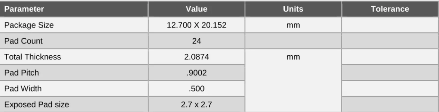
Table 2-1. ATBTLC1000-MR110 Module Information (1)
Parameter Value Units Tolerance
Package Size 12.700 X 20.152 mm
Pad Count 24
Total Thickness 2.0874 mm
Pad Pitch .9002
Pad Width .500
Exposed Pad size 2.7 x 2.7
ATBTLC1000-MR110CA [DATASHEET]
Atmel-42514D-ATBTLC1000-MR110CA-BLE-Module_Datasheet_032016 5
5
3
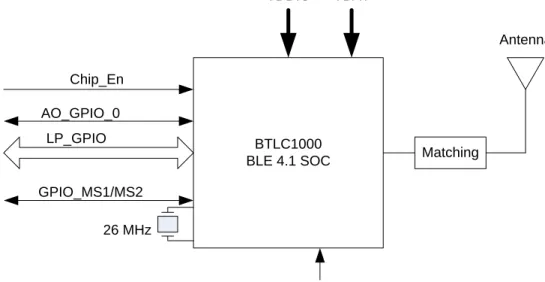
Block Diagram
Figure 3-1 shows the block diagram of the ATBTLC1000-MR110CA module.
Figure 3-1. Block Diagram
BTLC1000
BLE 4.1 SOC Matching
VDDIO VBAT Chip_En LP_GPIO AO_GPIO_0 Antenna 26 MHz From 32.768kHz crystal or clock GPIO_MS1/MS2
ATBTLC1000-MR110CA [DATASHEET]
Atmel-42514D-ATBTLC1000-MR110CA-BLE-Module_Datasheet_032016 6
6
4
Pin-out Information
4.1
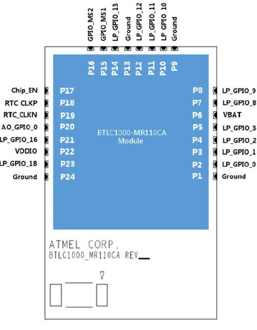
Pin Assignment
Figure 4-1 shows the module top view and pin numbering.
ATBTLC1000-MR110CA [DATASHEET]
Atmel-42514D-ATBTLC1000-MR110CA-BLE-Module_Datasheet_032016 7
7
4.2
Pin Description
Table 4-1 provides details for the module pin assignments and descriptions.
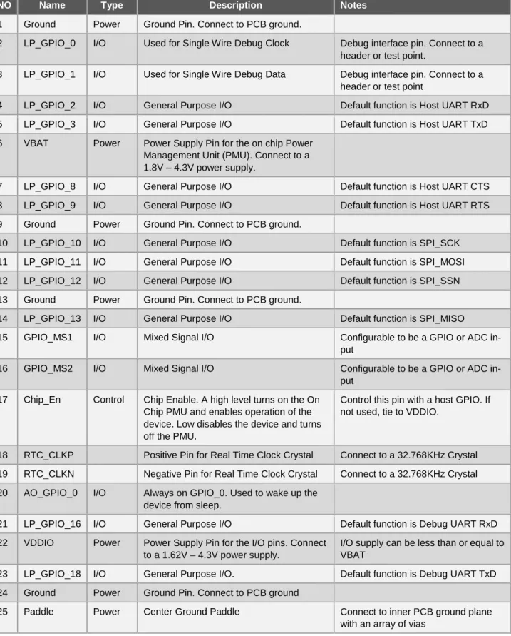
Table 4-1. Pin Description
NO Name Type Description Notes
1 Ground Power Ground Pin. Connect to PCB ground.
2 LP_GPIO_0 I/O Used for Single Wire Debug Clock Debug interface pin. Connect to a
header or test point.
3 LP_GPIO_1 I/O Used for Single Wire Debug Data Debug interface pin. Connect to a
header or test point
4 LP_GPIO_2 I/O General Purpose I/O Default function is Host UART RxD
5 LP_GPIO_3 I/O General Purpose I/O Default function is Host UART TxD
6 VBAT Power Power Supply Pin for the on chip Power
Management Unit (PMU). Connect to a 1.8V – 4.3V power supply.
7 LP_GPIO_8 I/O General Purpose I/O Default function is Host UART CTS
8 LP_GPIO_9 I/O General Purpose I/O Default function is Host UART RTS
9 Ground Power Ground Pin. Connect to PCB ground.
10 LP_GPIO_10 I/O General Purpose I/O Default function is SPI_SCK
11 LP_GPIO_11 I/O General Purpose I/O Default function is SPI_MOSI
12 LP_GPIO_12 I/O General Purpose I/O Default function is SPI_SSN
13 Ground Power Ground Pin. Connect to PCB ground.
14 LP_GPIO_13 I/O General Purpose I/O Default function is SPI_MISO
15 GPIO_MS1 I/O Mixed Signal I/O Configurable to be a GPIO or ADC
in-put
16 GPIO_MS2 I/O Mixed Signal I/O Configurable to be a GPIO or ADC
in-put 17 Chip_En Control Chip Enable. A high level turns on the On
Chip PMU and enables operation of the device. Low disables the device and turns off the PMU.
Control this pin with a host GPIO. If not used, tie to VDDIO.
18 RTC_CLKP Positive Pin for Real Time Clock Crystal Connect to a 32.768KHz Crystal
19 RTC_CLKN Negative Pin for Real Time Clock Crystal Connect to a 32.768KHz Crystal
20 AO_GPIO_0 I/O Always on GPIO_0. Used to wake up the
device from sleep.
21 LP_GPIO_16 I/O General Purpose I/O Default function is Debug UART RxD
22 VDDIO Power Power Supply Pin for the I/O pins. Connect to a 1.62V – 4.3V power supply.
I/O supply can be less than or equal to VBAT
23 LP_GPIO_18 I/O General Purpose I/O. Default function is Debug UART TxD
24 Ground Power Ground Pin. Connect to PCB ground
25 Paddle Power Center Ground Paddle Connect to inner PCB ground plane
ATBTLC1000-MR110CA [DATASHEET]
Atmel-42514D-ATBTLC1000-MR110CA-BLE-Module_Datasheet_032016 8
8
4.3
Module Outline Drawing
Figure 4-2 shows the view of the module and the module dimensions. All dimensions are in mm.
Figure 4-2. Module Dimensions (millimeters)
TOP VIEW P5 P4 P3 P2 P1 P6 P24 P20 P21 P22 P23 P19 P7 P8 P9 P10 P11 P12 P13 P14 P15 P16 P18 P17 BOTTOM VIEW SIDE VIEW PCB SHIELD
SOLDER PAD FOOTPRINT TOP VIEW BT LC 1000 _MR 110 C A R EV A TM E L C O R P . P1 P24 SHIELD
NOTE: THIS PAD MUST BE SOLDERED TO GND.
NOTE: THIS PAD MUST BE SOLDERED TO GND.
ATBTLC1000-MR110CA [DATASHEET]
Atmel-42514D-ATBTLC1000-MR110CA-BLE-Module_Datasheet_032016 9
9
5
Electrical Specifications
5.1
Absolute Maximum Ratings
This section describes the minimum and maximum ratings the module can tolerate.
Table 5-1. ATBTLC1000-MR110CA Absolute Maximum Ratings
Symbol Characteristics Min. Max. Unit
VDDIO I/O Supply Voltage -0.3 4.6 V
VBAT Battery Supply Voltage -0.3 5.0 V
VIN (1) Digital Input Voltage -0.3 VDDIO V
VAIN (2) Analog Input Voltage -0.3 1.5 V
VESDHBM (3) ESD Human Body Model -1000, -2000
(see notes below)
+1000, +2000 (see notes below)
V
TA Storage Temperature -65 150 °C
Junction Temperature 125 °C
Notes: 1. VIN corresponds to all the digital pins.
2. VAIN corresponds to the following analog pins: VDDRF_RX, VDDAMS, RFIO, XO_N, XO_P, VDD_SXDIG, VDD_VCO.
3. For VESDHBM, each pin is classified as Class 1, or Class 2, or both:
The Class 1 pins include all the pins (both analog and digital)
The Class 2 pins include all digital pins only
VESDHBM is ±1kV for Class1 pins. VESDHBM is ±2kV for Class2 pins.
5.2
Recommended Operating Conditions
Table 5-2. ATBTLC1000-MR110CA Recommended Operating Conditions
Symbol Characteristics Min. Typ. Max. Unit
VDDIO I/O Supply Voltage Low Range 1.62 1.80 4.3 V
VBAT Battery Supply Voltage 1.8 (1) 3.6 4.3 V
Operating Temperature -40 85 °C
Note: 1. VBAT supply must be greater than or equal to VDDIO.
5.3
Restrictions for Power States
When VDDIO is off (either disconnected or at ground potential), a voltage must not be applied to the device pins. This is because each pin contains an ESD diode from the pin to the VDDIO supply. This diode will turn ON when a voltage higher than one diode-drop is supplied to the pin. This in turn will try to power up the part through the VDDIO supply.
If a voltage must be applied to the signal pads while the chip is in a low power state, the VDDIO supply must be on.
Similarly, to prevent the pin-to-ground diode from turning on, do not apply a voltage that is more than 0.3V below ground to any pin.
ATBTLC1000-MR110CA [DATASHEET]
Atmel-42514D-ATBTLC1000-MR110CA-BLE-Module_Datasheet_032016 1
0 10
5.4
Power Sequences
Describes that sequence and parameters for powering up and down the device.
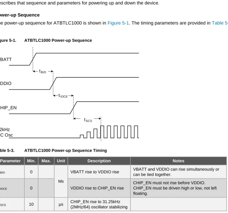
5.4.1 Power-up Sequence
The power-up sequence for ATBTLC1000 is shown in Figure 5-1. The timing parameters are provided in Table 5-3.
Figure 5-1. ATBTLC1000 Power-up Sequence
VBATT VDDIO CHIP_EN tBIO tIOCE 32kHz RC Osc tSCS
Table 5-3. ATBTLC1000 Power-up Sequence Timing
Parameter Min. Max. Unit Description Notes
tBIO 0
Ms
VBATT rise to VDDIO rise VBATT and VDDIO can rise simultaneously or can be tied together.
tIOCE 0 VDDIO rise to CHIP_EN rise
CHIP_EN must not rise before VDDIO. CHIP_EN must be driven high or low, not left floating.
tSCS 10 µs CHIP_EN rise to 31.25kHz
ATBTLC1000-MR110CA [DATASHEET]
Atmel-42514D-ATBTLC1000-MR110CA-BLE-Module_Datasheet_032016 1
1 11
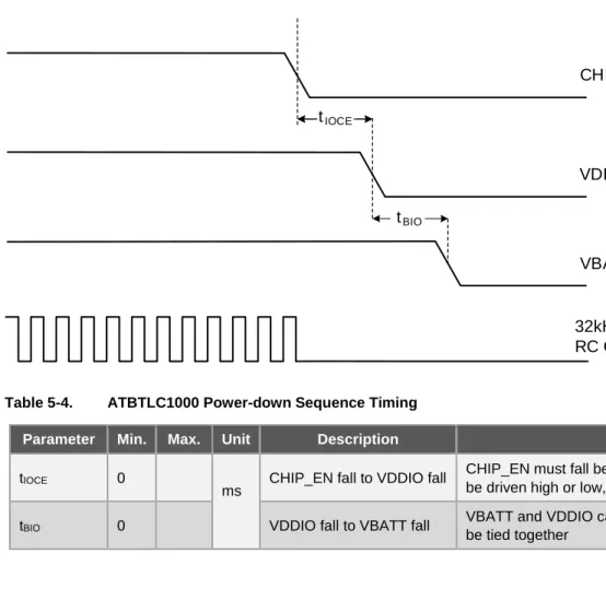
5.4.2 Power-down Sequence
The power-down sequence for ATBTLC1000 is shown in Figure 5-2. The timing parameters are provided in Table 5-5.
Figure 5-2. ATBTLC1000 Power-down Sequence
tIOCE 32kHz RC Osc CHIP_EN tBIO VBATT VDDIO
Table 5-4. ATBTLC1000 Power-down Sequence Timing
Parameter Min. Max. Unit Description Notes
tIOCE 0
ms CHIP_EN fall to VDDIO fall
CHIP_EN must fall before VDDIO. CHIP_EN must be driven high or low, not left floating
tBIO 0 VDDIO fall to VBATT fall
VBATT and VDDIO can fall simultaneously or can be tied together
5.5
Digital I/O Pin Behavior During Power-up Sequences
Table 5-5 describes the digital I/O Pin states corresponding to device power modes.
Table 5-5. Digital I/O Pin Behavior in Different Device States
Device state VDDIO CHIP_EN RESETN Output driver Input driver Pull-up/down
resistor (96kΩ)
Power_Down: core supply off High Low Low Disabled (Hi-Z) Disabled Disabled
Power-On Reset: core supply
on High High Low Disabled (Hi-Z) Disabled Enabled
Power-On Default: core sup-ply on, device out of reset but not programmed yet
High High High Disabled (Hi-Z) Enabled Enabled
Power-On Default: core sup-ply on, device out of reset but not programmed yet
High High High
Programmed by firmware for each pin: Ena-bled or DisaEna-bled Opposite of Output Driver state Programmed by firmware for each pin: Ena-bled or DisaEna-bled
ATBTLC1000-MR110CA [DATASHEET]
Atmel-42514D-ATBTLC1000-MR110CA-BLE-Module_Datasheet_032016 1
2 12
5.6
RTC Pins
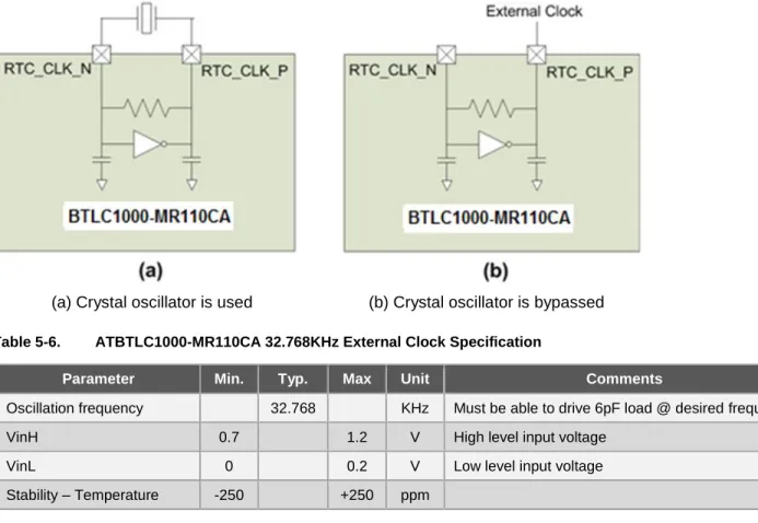
Module pins 18 and 19 (RTC_CLKP and RTC_CLKN, respectively) are used for a 32.768KHz crystal. To be compliant with the BLE specifications for connection events, the frequency accuracy of this clock has to be within ±500ppm. Because of the low drift of the 32.768kHz crystal oscillator clock and the fact that it can be accurately calibrated (±25ppm), the power consumption of the ATBTLC1000 can be minimized by leaving radio circuits in low power sleep mode for as long as possible until they need to wake up for the next connection timed event.
The block diagram in Figure 5-3(a) shows how the internal low frequency Crystal Oscillator (XO) is connected to the external crystal.
Typically, the crystal should be chosen to have a load capacitance of 7pF to minimize the oscillator current. Alternatively, if an external 32.768KHz clock is available, it can be used to drive the RTC_CLKP pin instead of using a crystal. The XO has 6pF internal capacitance on the RTC_CLKP pin. To bypass the crystal oscillator an external signal capable of driving 6pF can be applied to the RTC_CLK_P terminal as shown in Figure 5-3(b). This signal must be 1.2V maximum. RTC_CLK_N must be left unconnected when driving an external source into RTC_CLK_P.
Figure 5-3. ATBTLC1000 Connections to Low Frequency Crystal Oscillator
(a) Crystal oscillator is used (b) Crystal oscillator is bypassed
Table 5-6. ATBTLC1000-MR110CA 32.768KHz External Clock Specification
Parameter Min. Typ. Max Unit Comments
Oscillation frequency 32.768 KHz Must be able to drive 6pF load @ desired frequency
VinH 0.7 1.2 V High level input voltage
VinL 0 0.2 V Low level input voltage
ATBTLC1000-MR110CA [DATASHEET] Atmel-42514D-ATBTLC1000-MR110CA-BLE-Module_Datasheet_032016 1 3 13
6
Characteristics
6.1
Device States
Table 6-1. ATBTLC1000-MR110CA Device States
Device state CHIP_EN VDDIO IVBAT
(typical)
IVDDIO (typical)
Remarks
BLE_On_Transmit On On 3.0mA 0.0µA VBAT = 3.6V @ 0dBm Pout
BLE_On_Receive On On 4.2mA 0.0µA VBAT = 3.6V
Ultra Low Power On On 1.25µA 0.0µA With 8KB retention memory, BLE Timer and
RTC enabled
Power_Down GND On <0.05µA <0.05µA Chip Enable Off
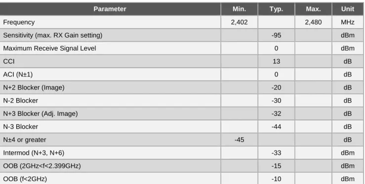
6.2
Receiver Performance
Table 6-2. ATBTLC1000-MR110CA Receiver Performance
Parameter Min. Typ. Max. Unit
Frequency 2,402 2,480 MHz
Sensitivity (max. RX Gain setting) -95 dBm
Maximum Receive Signal Level 0 dBm
CCI 13 dB
ACI (N±1) 0 dB
N+2 Blocker (Image) -20 dB
N-2 Blocker -30 dB
N+3 Blocker (Adj. Image) -32 dB
N-3 Blocker -44 dB
N±4 or greater -45 dB
Intermod (N+3, N+6) -33 dBm
OOB (2GHz<f<2.399GHz) -15 dBm
OOB (f<2GHz) -10 dBm
Note: Expected values for production silicon.
ATBTLC1000-MR110CA [DATASHEET]
Atmel-42514D-ATBTLC1000-MR110CA-BLE-Module_Datasheet_032016 1
4 14
6.3
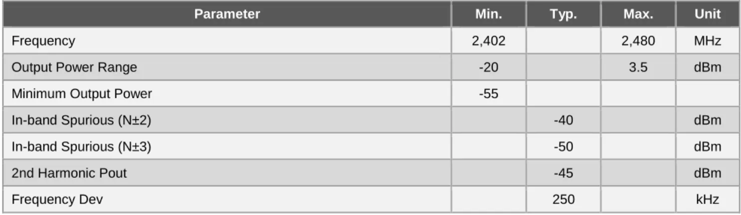
Transmitter Performance
Table 6-3. ATBTLC1000-MR110CA Transmitter Performance
Parameter Min. Typ. Max. Unit
Frequency 2,402 2,480 MHz
Output Power Range -20 3.5 dBm
Minimum Output Power -55
In-band Spurious (N±2) -40 dBm
In-band Spurious (N±3) -50 dBm
2nd Harmonic Pout -45 dBm
Frequency Dev 250 kHz
ATBTLC1000-MR110CA [DATASHEET]
Atmel-42514D-ATBTLC1000-MR110CA-BLE-Module_Datasheet_032016 1
5 15
7
Schematic Content
This chapter provides the schematic data for the ATBTLC1000 chip functionality on the ATBTLC1000-MR210 module. Module design information such as module schematics can be obtained under a NDA from Atmel.
7.1
Application Schematic
The ATBTLC1000-MR110 module is fully self-contained. To use the module, just provide VBAT and VDDIO supplies. Figure 7-1 shows a typical design using the ATBTLC1000-MR110 module. The schematic shows several host interfaces: UART with Flow Control (4-wire) and SPI as well as an input to the ADC on the GPIO_MS2 pin. A user can choose the interface(s) required for their application. If a 32.768KHz Real Time Clock is not available in the system, a 32.768KHz crystal can be used. Figure 7-2 shows a design using a crystal for the Real Time Clock. The crystal should be specified with a load capacitance, CL=7pF and a total frequency error of 200ppm.
ATBTLC1000-MR110CA [DATASHEET]
Atmel-42514D-ATBTLC1000-MR110CA-BLE-Module_Datasheet_032016 1
6 16
ATBTLC1000-MR110CA [DATASHEET]
Atmel-42514D-ATBTLC1000-MR110CA-BLE-Module_Datasheet_032016 1
7 17
8
Placement and Routing Guidelines
It is critical to follow the recommendations listed below to achieve the best RF performance:
The board should have a solid ground plane. The center ground pad of the device must be solidly connected to the ground plane by using a 3 x 3 grid of vias. Each ground pin of the module should have a ground via placed either in the pad or right next to the pad going down to the ground plane.
When the module is placed on the motherboard, a provision for the antenna must be made. There should be nothing under the portion of the module, which contains the antenna. This means the antenna should not be placed directly on top of the motherboard PCB. This can be accomplished by, for example, placing the module at the edge of the board such that the module edge with the antenna extends beyond the main board edge by 6.5mm. Alternatively, a cutout in the motherboard can be provided under the antenna. The cutout should be at least 22mm x 6.5mm. Ground vias spaced 2.5mm apart should be placed all around the perimeter of the cutout. No large components should be placed near the antenna.
Keep away from antenna, as far as possible, large metal objects to avoid electromagnetic field blocking Do not enclose the antenna within a metal shield
Keep any components which may radiate noise or signals within the 2.4GHz – 2.5GHz frequency band far away from the antenna or better yet, shield those components. Any noise radiated from the main board in this frequency band will degrade the sensitivity of the module.
8.1
Power and Ground
Dedicate one layer as a ground plane. Make sure that this ground plane does not get broken up by routes. Power can route on all layers except the ground layer. Power supply routes should be heavy copper fill planes to insure the lowest possible inductance. The power pins of the module should have a via directly to the power plane as close to the pin as possible. Decoupling capacitors should have a via right next to the capacitor pin and this via should go directly down to the power plane – that is to say, the capacitor should not route to the power plane through a long trace. The ground side of the decoupling capacitor should have a via right next to the pad which goes directly down to the ground plane. Each decoupling capacitor should have its own via directly to the ground plane and directly to the power plane right next to the pad. The decoupling capacitors should be placed as close to the pin that it is filtering as possible.
ATBTLC1000-MR110CA [DATASHEET]
Atmel-42514D-ATBTLC1000-MR110CA-BLE-Module_Datasheet_032016 1
8 18
9
Interferers
One of the biggest problems with RF receivers is poor performance due to interferers on the board radiating noise into the antenna or coupling into the RF traces going to input LNA. Care must be taken to make sure that there is no noisy circuitry placed anywhere near the antenna or the RF traces. All noise generating circuits should also be shielded so they do not radiate noise that is picked up by the antenna. Also, make sure that no traces route underneath the RF portion of the ATBTLC1000. Also, make sure that no traces route underneath any of the RF traces from the antenna to the ATBTLC1000 input. This applies to all layers. Even if there is a ground plane on a layer between the RF route and another signal, the ground return current will flow on the ground plane and couple into the RF traces.
ATBTLC1000-MR110CA [DATASHEET]
Atmel-42514D-ATBTLC1000-MR110CA-BLE-Module_Datasheet_032016 1
9 19
10
Reference Documentation and Support
10.1 Reference Documents
Atmel offers a set of collateral documentation to ease integration and device ramp.
The following list of documents available on Atmel web or integrated into development tools.
Title Content
Datasheet This document
ATBTLC1000 SOC Datasheet
Data sheet for the ATBTLC1000 SOC contained on this module.
SW Design Guide Integration guide with clear description of: High level Arch, overview on how to write a networking application, list all API, parameters and structures. Features of the device, SPI/handshake protocol between device and host MCU, with flow/sequence/state diagram, timing.
SW Programmer guide
Explain in details the flow chart and how to use each API to implement all generic use cases (e.g. start AP, start STA, provisioning, UDP, TCP, http, TLS, p2p, errors management, connec-tion/transfer recovery mechanism/state diagram) - usage and sample application note
ATBTLC1000-MR110CA [DATASHEET] Atmel-42514D-ATBTLC1000-MR110CA-BLE-Module_Datasheet_032016 2 0 20
11
Certifications
11.1 Agency Compliance
The ATBTLC1000-MR110CA has been tested and certified to meet the compliance for the following agencies: Bluetooth 4.1
– QD ID Controller (see declaration D028678)
– QD ID Host (see declaration D028679) FCC – FCC ID: 2ADHKBTLC1000 CFR47 Part 15 ETSI – EN 300 328 – EN 300 400 Class 2 ARIB – STD-T66 TELEC
ATBTLC1000-MR110CA [DATASHEET]
Atmel-42514D-ATBTLC1000-MR110CA-BLE-Module_Datasheet_032016 2
1 21
12
Reflow Profile Information
This chapter provides guidelines for reflow processes in getting the Atmel module soldered to the customer’s design.
12.1 Storage Condition
12.1.1 Moisture Barrier Bag Before Opened
A moisture barrier bag must be stored in a temperature of less than 30°C with humidity under 85% RH. The calculated shelf life for the dry-packed product shall be 12 months from the date the bag is sealed.
12.1.2 Moisture Barrier Bag Open
Humidity indicator cards must be blue, <30%.
12.2 Stencil Design
The recommended stencil is laser-cut, stainless-steel type with thickness of 100µm to 130µm, and approximately a 1:1 ratio of stencil opening to pad dimension. To improve paste release, a positive taper with bottom opening 25µm larger than the top can be utilized. Local manufacturing experience may find other combinations of stencil
thickness and aperture size to get good results.
12.3 Baking Conditions
This module is rated at MSL level 3. After the sealed bag is opened, no baking is required within 168 hours so long as the devices are held at ≤30°C/60% RH or stored at <10% RH.
The module will require baking before mounting if: The sealed bag has been open for >168 hours Humidity Indicator Card reads >10%
SIPs need to be baked for 8 hours at 125°C
12.4 Soldering and Reflow Condition
12.4.1 Reflow Oven
It is strongly recommended that a reflow oven equipped with more heating zones and Nitrogen atmosphere be used for lead-free assembly. Nitrogen atmosphere has shown to improve the wet-ability and reduce temperature gradient across the board. It can also enhance the appearance of the solder joints by reducing the effects of oxidation.
The following bullet items should also be observed in the reflow process:
Some recommended pastes include NC-SMQ® 230 flux and Indalloy® 241 solder paste made up of 95.5
Sn/3.8 Ag/0.7 Cu or SENJU N705-GRN3360-K2-V Type 3, no clean paste.
Allowable reflow soldering times: Three times based on the following reflow soldering profile (see Figure 12-1).
Temperature profile: Reflow soldering shall be done according to the following temperature profile (see
Figure 12-1). Peak temp: 250°C.
ATBTLC1000-MR110CA [DATASHEET]
Atmel-42514D-ATBTLC1000-MR110CA-BLE-Module_Datasheet_032016 2
2 22
ATBTLC1000-MR110CA [DATASHEET]
Atmel-42514D-ATBTLC1000-MR110CA-BLE-Module_Datasheet_032016 2
3 23
13
Errata
Issue: The measured current for the device state cases listed in Table 6-1 will be higher than what is reported in
the table.
This is because the Power number values in the SDK4.0 release have not been fully optimized to their final values.
A small sample measurement has been performed on 10 samples and they show the following results: Measurement condition:
1-sec adverting interval
37 byte advertising payload
Connectable beacon
Advertising on three channels (37, 38,and 39)
Vbatt and VDDIO are set to 3.3V
SAM L21 has a measurement floor of 80nA which was compensated in the reported numbers (this number varies from board to board and needs to be compensated).
The Average advertising current: 11.3µA
The Average sleep current between beacons: 1.17µA
The average current for the 10 boards was (including 80nA floor):
Sample #
1
2
3
4
5
6
7
8
9
10
Average Current (µA)
11.55 11.45 11.45
11.7
11.4
11.25 10.95
11.2
11.6
11.4
Work around: Will be resolved in a SDK update.
For a complete listing of development-support tools and documentation, visit http://www.atmel.com/ or contact the nearest Atmel field representative.
ATBTLC1000-MR110CA [DATASHEET]
Atmel-42514D-ATBTLC1000-MR110CA-BLE-Module_Datasheet_032016 2
4 24
14
Revision History
Doc Rev. Date Comments
42514D 03/2106
1. Corrected package table ground pad size in Table 2-1. 2. Updated module drawing in Figure 4-2.
3. Corrected Errata to refer to Table 6-1. 4. Revised reflow recurrence in Section 13.
42514C 12/2015
1. Updated performance numbers. 2. Added UART Flow Control. 3. Added clearer diagrams.
4. Added Agency Certification section.
5. Corrected Package size value in Order information Chapter 1. 6. Updated Module Drawing figure in Section 4.3.
7. Revised Schematic content Chapter 7. 8. Added Reflow Profile Chapter 12. 9. Added Errata Chapter 13.
42514B 07/2015 Updated for B0 silicon
ATBTLC1000-MR110CA [DATASHEET]
Atmel-42514D-ATBTLC1000-MR110CA-BLE-Module_Datasheet_032016 2
5 25
Atmel Corporation 1600 Technology Drive, San Jose, CA 95110 USA T: (+1)(408) 441.0311 F: (+1)(408) 436.4200 │ www.atmel.com © 2016 Atmel Corporation. / Rev.: Atmel-42514D-ATBTLC1000-MR110CA-BLE-Module_Datasheet_032016.
Atmel®, Atmel logo and combinations thereof, Enabling Unlimited Possibilities®, and others are registered trademarks or trademarks of Atmel Corporation in U.S. and
other countries. ARM®, ARM Connected® logo, Cortex®, and others are the registered trademarks or trademarks of ARM Ltd. Other terms and product names may be
trademarks of others.
DISCLAIMER: The information in this document is provided in connection with Atmel products. No license, express or implied, by estoppel or otherwise, to any intellectual property right is granted by this document or in connection with the sale of Atmel products. EXCEPT AS SET FORTH IN THE ATMEL TERMS AND COND ITIONS OF SALES LOCATED ON THE ATMEL WEBSITE, ATMEL ASSUMES NO LIABILITY WHATSOEVER AND DISCLAIMS ANY EXPRESS, IMPLIED OR STATUTORY WARRANTY RELATING TO ITS PRODUCTS INCLUDING, BUT NOT LIMITED TO, THE IMPLIED WARRANTY OF MERCHANTABILITY, FITNESS FOR A PARTICULAR PURPOSE, OR NON -INFRINGEMENT. IN NO EVENT SHALL ATMEL BE LIABLE FOR ANY DIRECT, INDIRECT, CONSEQUENTIAL, PUNITIVE, SPECIAL OR INCIDENTAL DAMAGES (INCLUDING, WITHOUT LI MITATION, DAMAGES FOR LOSS AND PROFITS, BUSINESS INTERRUPTION, OR LOSS OF INFORMATION) ARISING OUT OF THE USE OR INABILITY TO USE THIS DOCUMENT, EVEN IF ATMEL HAS BEEN ADVISED OF THE POSSIBILITY OF SUCH DAMAGES. Atmel makes no representations or warranties with respect to the accurac y or completeness of the contents of this document and reserves the right to make changes to specifications and products descriptions at any time without notice. Atmel does not make any commitment to update the information contained herein. Unless specifically provided otherwise, Atmel products are not suitable for, and shall not be use d in, automotive applications. Atmel products are not intended, authorized, or warranted for use as components in applications intended to support or sustain life.
SAFETY-CRITICAL, MILITARY, AND AUTOMOTIVE APPLICATIONS DISCLAIMER: Atmel products are not d esigned for and will not be used in connection with any applications where the failure of such products would reasonably be expected to result in significant personal injury or death (“Safety -Critical Applications”) without an Atmel officer's specific written consent. Safety-Critical Applications include, without limitation, life support devices and systems, equipment or systems for the operation o f nuclear facilities and weapons systems. Atmel products are not designed nor intended for use in military or a erospace applications or environments unless specifically designated by Atmel as military -grade. Atmel products are not designed nor intended for use in automotive applications unless specifically designated by Atmel as automotive -grade.