International Journal of Advanced Engineering Research and Science (IJAERS) [Vol-3, Issue-12, Dec- 2016]
https://dx.doi.org/10.22161/ijaers/3.12.4 ISSN: 2349-6495(P) | 2456-1908(O)
www.ijaers.com Page | 20
A Modified Method for Tuning PID Controller
for Buck-Boost Converter
Muhanad D. Almawlawe
1, Marko Kovandzic
21Engineering Collage ,AL-Qadisiya University , Iraq 2
Department of Mechatronic and Control, Faculty of Mechanical Engineering , University of Niš , Republic of Serbia
Abstract— This paper presents a design and simulation of simplified method for designing a proportional –
integral–derivative(PID)controller operating in
continuous conduction mode for the Buck-Boost converter ,this method provides good voltage regulation and is suitable for Buck-Boost Dc-Dc converter, it is exposed to significant variations which may take this system away from nominal conditions caused by the line change and parameters variation at the input .Simulation results shows that this PID controller provides good voltage regulation and is suitable for the Buck-Boost purposes. The obtained results prove the robustness of proposed Controller against variation of the input voltage ,load resistance and the referent voltage of the studied converter.
Keywords— Buck-Boost converter , Proportional- integral-derivative (PID)controller , Continuous Conduction Mode (CCM) , Pulse Width Modulation(PWM) .
I. INTRODUCTION
The voltage Converter is an electrical circuit that is used to control the transfer of energy between the source and the consumer . The need for a broad spectrum of consumer's cabinets caused the development of different types of converters. The scope of current ranges moves within the limits order of several hundred mili amperes to several hundred amperes . Converters differ according to the principle of functioning, construction, energy efficiency, size, precision control , transitional state response , and of course the price. Converter usually has an additional feature to provide protection in the event of system failure, All regulators have a power transfer stage and a control circuitry to sense the output voltage and adjust the power transfer stage to maintain the constant output voltage. Since a feedback loop is necessary to maintain regulation, some type of compensation is required to maintain loop stability [1].
The Dc-Dc converter is a type of these regulators which are used to convert the Dc voltage from one level to another level such that the output voltage must be regulated with respect to the disturbances [2]. From this electrical device is expected to provide a stable voltage
for a wide range of power output. The voltage must remain immutable and for a wide range of input voltage, which in practice inevitably occurs as a consequence of the discharge when the battery used as a source of electrical energy [3]. Because of positive characteristics of Dc-Dc converters they can be used as an integral part of the device for utilization of alternative and renewable energy sources, portable devices and many industrial processes, as an examples of the use of Dc-Dc converters in modern technology computer systems, communications equipment, micro electromechanical systems (MEMS) devices for welding, Dc motors [3,4]. In solar power systems the converters allows connection of photovoltaic cells on consumer electrical power grid thus avoiding the use of batteries [5].
The development of power electronics has enabled the use of non-isolating Dc-Dc converters, i.e without using transformers, the advantage of these converters reduces the cost and increases the efficiency of these devices, so while transferring energy small losses we have because of the significant amount of heat , i.e there is no need for intensive cooling. The basic idea of the controlling procedure is dominated by electronically controlling the pulses that regulate the switch of the converters resulting a great efficiency( which ranges up to 98%),or in other words electronically controlling the pulse width (Pulse-Width Modulation PWM)[6]. The switch enables the passage of the current from input to the output. Within the time that elapses between two successive pulses, called commutation cycle, the switch is turned on for a while and then off to the end of the cycle. By appropriately adjusting the relationship between the period of the pulse (when the switch is turned on) with respect to total duration of the cycles , we have the so called duty cycle d , by which we can set the output voltage of the converter, Setting of the converter is based on feedback stage that ensures that the output voltage tends asymptotically to the reference value regardless of disturbances [4]. The negative feature of these converters is the existence of variations in output current as a result of the switching action, but this is simply overcomes by applying filters[7].
https://dx.doi.org/10.22161/ijaers/3.12.4 ISSN: 2349-6495(P) | 2456-1908(O)
Depending on the topologies of the switching Dc-Dc converters ,we have different types of converters, the basic topologies are Boost (Step Up) converter, Buck (step down) , Buck-Boost (step up/down ) , the designing procedure of Buck-Boost Converter is complex procedure due to the presence of nonlinearities, so it is not possible to directly apply simple methods for designing the controller , so we develop a different strategy for modeling processes, each of them has its advantages and disadvantages, and accordingly finds its application field [7-18]. This paper discusses the possibility of designing PID (proportional integral differential) controller, as the most affordable ,and in practice ,is the most widely vision for control. Modeling was considered in continuous conductive mode taking into account the parasitic resistances in the circuit . The simulation is done using the MATLAB/ Simulink environment .
The paper is organized as following : In the second section, the mathematical model of Buck-Boost Dc-Dc converter is discussed , the third section deals with the controller design procedure , the fourth section consider the simulation process , the last section contains conclusion and some remarks .
II. MATEMATICALMODEL
Controller design for any system needs knowledge about system behavior ,usually this involves a mathematical description of the relation among inputs to the process, state variables, and output. This description in the form of mathematical equations which describe behavior of the system (process) is called model of the system . Using Fig .1 we can find the differential equation when the switch is closed : Fig.1:Buck-Boost circuit , 0 ( ) C C C L E L P L dV V C dt R R t dT dI L V R R I dt = − + < < = − + (1)
The state space equation based on the previous system of equations can be represented :
( )
( )
( )
( )
( )
z E R z t t V t V t C t = + = & z x A x B x (2) Where :(
1)
0 0 0 1 0 c z z c L P C R R R C R R R R L L − + = = = + + − z A B (3)And when is opened the differential equation is now :
(
) (
)
(
)
, ( | | ) C C L c c L C c L D L c dV V R C I dt R R R R dT t T dI R L V R R R R I dt R R = − + + + < < = − + − − + (4)The state space equation is now :
( )
( )
( )
( )
( )
o o E R o t A x t V t V t C t = + = & x B x (5) Where :(
)
(
)
(
)
1 0 || || 0 c c o o c c L D c c R C R R C R R R C R R R R R R R R R L R R L − + + = = = − − + − + A B (6)One strategy for obtaining a single mathematical model may be the introduction of the duty cycles d, this approach allows combining state equation for the previous two cases, according to the principle of averaging model in state space [14]. On this occasion, the nonlinearity caused by the switch was overcome and the system’s equivalent model in state space [7] , we have :
( )
( )
( )
( )
( )
E R t x t V t V t C t = + = & x A B x (7) Where :(
)
(
( )
)
( )
(
)
( )
( )
1 1 1 1 ( || ) 0 1 || c C c D L P c c c R d C R R C R R R d d R R R R dR L R R L R C d R R R R d L − − + + = − − − − − − + = = − + A B (8)International Journal of Advanced Engineering Research and Science (IJAERS) https://dx.doi.org/10.22161/ijaers/3.12.4
www.ijaers.com
Applying the Laplace transform to the previous system we obtain the transfer function between the values of the input and output :
( ) ( )( ) (( )) ( )
(
2 2 1 * 1 1 1 1 1 * 1 1 1 R C E C C C V s d d C s G s R V s LC s s d RC L LC α β α α α − + = == + + − + − − + + Where :(
)
(
)
(
(
)(
) (
)(
)
1 1 1 1 1 1 , , , 1 1 C L C L C C L C C L C D S L C D S C D L P C d R R R R R R R R d d α α α α α α α α α α α α α β α α α α α − + + − + − + + = − = = = = = − − − + +Voltage amplification in steady state [8,9,10,11,12,13] is :
(
)
2 1 1 1 1 C d M d d α β + = − − −III. CONTROLLERDESIGNPROCEDURE
The basic control equation for the PID controller is giving in [14 , 15, 16]:
( )
p( )
i( )
d( )
de t u t K e t K e t dt K dt = + ∫ +And its transfer function is :
( )
( )
( )
1 1 i p d p d U s K C s K K s K sT E s s sT = = + + = + + where K , p K , and i K are the proportional , integral d
and differential gains, respectively, and constants
p i K T Ki = and d d p K T K = .
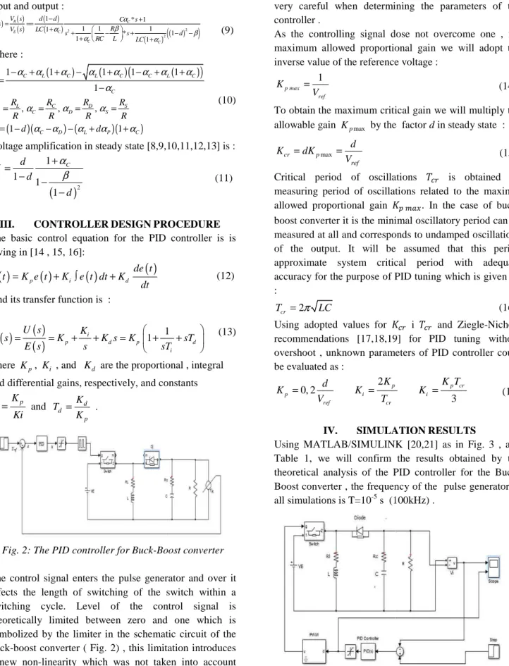
Fig. 2: The PID controller for Buck-Boost converter
The control signal enters the pulse generator and over it affects the length of switching of the switch within a switching cycle. Level of the control signal is theoretically limited between zero and one which is symbolized by the limiter in the schematic circuit of the buck-boost converter ( Fig. 2) , this limitation introduces a new non-linearity which was not taken into account when deriving the mathematical model (8) and the transfer function of the system (9) . Level of the control signal out of range of the limiter will have the limit
International Journal of Advanced Engineering Research and Science (IJAERS) ISSN: 2349
Applying the Laplace transform to the previous system we obtain the transfer function between the values of the
( )
(
2)
* 1 s+ − s+ −d −β (9)(
)
)
1−α αC+ L 1+αC − αL 1+αC 1−α αC+ L 1+αC (10)Voltage amplification in steady state [8,9,10,11,12,13] is :
(11)
PROCEDURE
The basic control equation for the PID controller is is
(12) 1 p d p d i C s K K s K sT E s s sT = = + + = + + (13)
are the proportional , integral and differential gains, respectively, and constants
Boost converter
The control signal enters the pulse generator and over it affects the length of switching of the switch within a control signal is theoretically limited between zero and one which is symbolized by the limiter in the schematic circuit of the boost converter ( Fig. 2) , this limitation introduces linearity which was not taken into account he mathematical model (8) and the transfer function of the system (9) . Level of the control signal out of range of the limiter will have the limit
values or the system becomes insensitive to further change in the error signal. Due to this fact we should very careful when determining the parameters of the controller .
As the controlling signal dose not overcome one , for maximum allowed proportional gain we will adopt the inverse value of the reference voltage :
1 p max ref K V =
To obtain the maximum critical gain we will multiply the allowable gain Kpmax by the factor
max cr p ref d K dK V = =
Critical period of oscillations
measuring period of oscillations related to the maximal allowed proportional gain
boost converter it is the minimal oscillatory period can be measured at all and corresponds to undamped oscillations of the output. It will be assumed that this period approximate system critical period with adequate accuracy for the purpose of PID tuning which is given by :
2 cr
T =
π
LCUsing adopted values for
recommendations [17,18,19] for PID tuning without overshoot , unknown parameters of PID controller could be evaluated as : 2 0, 2 p p cr p i i ref cr K K T d K K K V T = = = IV. SIMULATION Using MATLAB/SIMULINK [20,21] as i
Table 1, we will confirm the results obtained by the theoretical analysis of the PID controller for the Buck Boost converter , the frequency of the pulse generator in all simulations is T=10-5 s (100kHz)
Fig. 3: The Simulink model of with PID controller.
[Vol-3, Issue-12, Dec- 2016]
ISSN: 2349-6495(P) | 2456-1908(O)
Page | 22
values or the system becomes insensitive to further change in the error signal. Due to this fact we should be very careful when determining the parameters of the
As the controlling signal dose not overcome one , for maximum allowed proportional gain we will adopt the inverse value of the reference voltage :
(14)
To obtain the maximum critical gain we will multiply the by the factor d in steady state :
(15)
Critical period of oscillations is obtained by
measuring period of oscillations related to the maximal . In the case of buck-boost converter it is the minimal oscillatory period can be measured at all and corresponds to undamped oscillations utput. It will be assumed that this period approximate system critical period with adequate accuracy for the purpose of PID tuning which is given by
(16) i and Ziegle-Nichols recommendations [17,18,19] for PID tuning without overshoot , unknown parameters of PID controller could
0, 2 3 p p cr p i i K K T K = K = K = (17) SIMULATIONRESULTS
Using MATLAB/SIMULINK [20,21] as in Fig. 3 , and Table 1, we will confirm the results obtained by the theoretical analysis of the PID controller for the Buck-Boost converter , the frequency of the pulse generator in
(100kHz) .
The Simulink model of the buck-boost converter with PID controller.
https://dx.doi.org/10.22161/ijaers/3.12.4
Table.1: Parameters of Buck-Boost converter circuit Element physical Value
Coil Inductance resistance Capacitor Capacitance resistance Load resistance resistance Diode resistance Switch resistance
Output volt Proposed Voltage
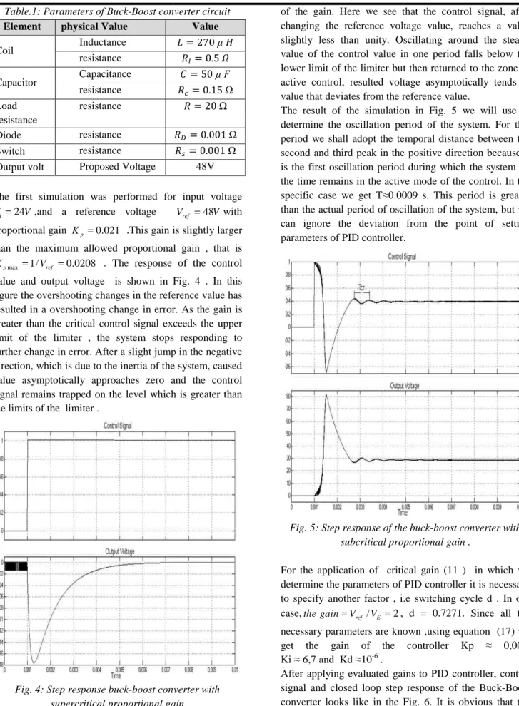
The first simulation was performed for input voltage 24
i
V = V ,and a reference voltage
proportional gain Kp =0.021 .This gain is slightly larger than the maximum allowed proportional
max 1/ 0.0208
p ref
K = V = . The response of the control
value and output voltage is shown in Fig. 4 . figure the overshooting changes in the reference value has resulted in a overshooting change in error. As the gain is greater than the critical control signal exceeds the upper limit of the limiter , the system stops responding to further change in error. After a slight jump in the negative direction, which is due to the inertia of the system, caused value asymptotically approaches zero and the control signal remains trapped on the level which is greater than the limits of the limiter .
Fig. 4: Step response buck-boost converter with supercritical proportional gain
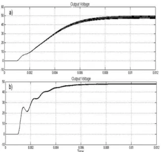
In the second simulation the proportional gain value Kp = 0.0205, which is slightly less than the critical value
ISSN: 2349 Boost converter circuit
Value 270 µ 0.5 50 µ 0.15 Ω 20 Ω 0.001 Ω 0.001 Ω 48V
The first simulation was performed for input voltage and a reference voltage Vref =48V with .This gain is slightly larger maximum allowed proportional gain , that is . The response of the control put voltage is shown in Fig. 4 . In this the overshooting changes in the reference value has resulted in a overshooting change in error. As the gain is greater than the critical control signal exceeds the upper limit of the limiter , the system stops responding to slight jump in the negative direction, which is due to the inertia of the system, caused value asymptotically approaches zero and the control signal remains trapped on the level which is greater than
boost converter with supercritical proportional gain
In the second simulation the proportional gain value Kp = 0.0205, which is slightly less than the critical value
of the gain. Here we see that the control signal, after changing the reference voltage value, reaches a value slightly less than unity. Oscillating around the steady value of the control value in one period falls below the lower limit of the limiter but then returned to the zone of active control, resulted voltage asymptotically tend value that deviates from the reference value.
The result of the simulation in Fig. 5 we will use to determine the oscillation period of the system. For this period we shall adopt the temporal distance between the second and third peak in the positive
is the first oscillation period during which the system all the time remains in the active mode of the control. In the specific case we get T≈0.0009 s. This period is greater than the actual period of oscillation of the system, but we can ignore the deviation from the point of setting parameters of PID controller
Fig. 5: Step response of the buck
subcritical proportional gain .
For the application of critical gain (11 ) in which we determine the parameters of P
to specify another factor , i.e switching cycle d . In our case,the gain=Vref /VE =2,
necessary parameters are known ,using equation (17) we get the gain of the
Ki ≈ 6,7 and Kd ≈10-6 .
After applying evaluated gains to PID controller, control signal and closed loop step response of the Buck converter looks like in the Fig. 6. It is obvious that the aim is fulfilled. The control signal never l
saturation element. After initial bounce, limited by adopted gain, it uniformly raises until reaches level of the
ISSN: 2349-6495(P) | 2456-1908(O)
of the gain. Here we see that the control signal, after voltage value, reaches a value slightly less than unity. Oscillating around the steady value of the control value in one period falls below the lower limit of the limiter but then returned to the zone of active control, resulted voltage asymptotically tends to value that deviates from the reference value.
The result of the simulation in Fig. 5 we will use to determine the oscillation period of the system. For this period we shall adopt the temporal distance between the second and third peak in the positive direction because it is the first oscillation period during which the system all the time remains in the active mode of the control. In the
≈0.0009 s. This period is greater than the actual period of oscillation of the system, but we can ignore the deviation from the point of setting
.
Step response of the buck-boost converter with subcritical proportional gain .
For the application of critical gain (11 ) in which we determine the parameters of PID controller it is necessary to specify another factor , i.e switching cycle d . In our
/ 2 d = 0.7271. Since all the
necessary parameters are known ,using equation (17) we
controller Kp ≈ 0,003, After applying evaluated gains to PID controller, control
signal and closed loop step response of the Buck-Boost converter looks like in the Fig. 6. It is obvious that the aim is fulfilled. The control signal never lefts scope of the saturation element. After initial bounce, limited by adopted gain, it uniformly raises until reaches level of the
International Journal of Advanced Engineering Research and Science (IJAERS) https://dx.doi.org/10.22161/ijaers/3.12.4
www.ijaers.com
duty cycle d. The output voltage grows, also without oscillations, before it comes to referent value. The raising time is approximately 8 ms .
The next few simulations investigate robustness of designed PID control of Buck-Boost converter to uncertainty of system parameters. The first subject of observation is input voltage V , while E
minimal input voltage is VE =17, 32V
confirms slightly higher value of input voltage, due system stays stable (about 18,3 V) .
Fig. 6: Step response of the Buck-Boost converter with PID control.
Fig. 7a show step response of the output voltage for the input voltage VE =17.32V. The shape of the response and settling time stay almost unchanged. The result of simulation in Fig. 7b, obtained for the input voltage of
96 E
V = V, and the same output voltage, shows
oscillations in step response of output voltage while the settling time is slightly reduced. Input voltage, in the practice, doesn’t reach such level of uncertainty, especially in positive direction. Thus, curren configuration should be considered as stable for the positive disturbances of input voltage and below limited by maximal gain.
International Journal of Advanced Engineering Research and Science (IJAERS) ISSN: 2349
duty cycle d. The output voltage grows, also without oscillations, before it comes to referent value. The raising
The next few simulations investigate robustness of Boost converter to uncertainty of system parameters. The first subject of
48 ref
V = V ,the
17, 32
V V . Simulation
confirms slightly higher value of input voltage, due
Boost converter with
Fig. 7a show step response of the output voltage for the . The shape of the response and settling time stay almost unchanged. The result of simulation in Fig. 7b, obtained for the input voltage of , and the same output voltage, shows oscillations in step response of output voltage while the settling time is slightly reduced. Input voltage, in the practice, doesn’t reach such level of uncertainty, especially in positive direction. Thus, current PID configuration should be considered as stable for the positive disturbances of input voltage and below limited
Fig.7: The step response of the Buck
with PID control: a) VE
The next simulation consider the case when the reference voltage is variable ,the input voltage of
reference voltage of Vref =1V
is obvious the negative effect of reference vol reduction to the settling time. In the current simulation it is about 40 ms which is 5 times longer than settling time in the case of nominal reference voltage (8 ms). The upper limit of reference voltage is caused by maximal gain of the Buck-Boost converter. Fig. 8b , shows step response of output voltage
parameters of the controller, and for the reference voltage of Vref =60V , slightly lower than maximal possible. It can be noticed amplification of oscillations but decreasing of settling time, although the control system stays completely operational.
Fig. 8 The step response of the Buck
PID control: a) Vref = 1 V, b) Vref = 60 V [Vol-3, Issue-12, Dec- 2016]
ISSN: 2349-6495(P) | 2456-1908(O)
Page | 24 The step response of the Buck-Boost converter
with PID control: a) VE = 18.3 V, b) VE = 96V
The next simulation consider the case when the reference voltage is variable ,the input voltage of VE =24V and
1
V V as it is shown in Fig. 8a. It
is obvious the negative effect of reference voltage reduction to the settling time. In the current simulation it is about 40 ms which is 5 times longer than settling time in the case of nominal reference voltage (8 ms). The upper limit of reference voltage is caused by maximal nverter. Fig. 8b , shows step
response of output voltage V , due to the same R
parameters of the controller, and for the reference voltage , slightly lower than maximal possible. It amplification of oscillations but decreasing of settling time, although the control system stays
Fig. 8 The step response of the Buck-Boost converter with PID control: a) Vref = 1 V, b) Vref = 60 V
https://dx.doi.org/10.22161/ijaers/3.12.4
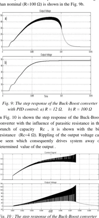
The next simulation examine the influence of output resistance uncertainty to the control system behavior Fig. 9 which is done with the constant input voltage of
24 E
V = V and reference voltage of
Compared to the two previous cases, very similar conclusions are obtained. The value of the output resistance such that the system remains stable is about 12.7Ω , as the output resistance decreases the maximal gain also decreases. For the resistance belo
value, maximal output voltage of 48 V goes out the range and output voltage fails in following reference voltage Fig. 9a . The system robustness for the positive change of output resistance is much higher, step response of the control system for the output resistance 5 times higher than nominal (R=100 Ω) is shown in the Fig. 9b.
Fig. 9: The step response of the Buck-Boost converter
with PID control: a) R = 12 Ω, b) R = 100
In Fig. 10 is shown the step response of the Buck converter with the influence of parasitic resistance in the brunch of capacity Rc , it is shown with the big resistance (Rc=4 Ω). Rippling of the output voltage can be seen which consequently drives system away of determined value of the output .
Fig. 10 : The step response of the Buck-Boost converter with great resistance in the branch capacitor
ISSN: 2349
the influence of output resistance uncertainty to the control system behavior
which is done with the constant input voltage of
and reference voltage of Vref =48V .
Compared to the two previous cases, very similar conclusions are obtained. The value of the output resistance such that the system remains stable is about , as the output resistance decreases the maximal gain also decreases. For the resistance below minimum value, maximal output voltage of 48 V goes out the range and output voltage fails in following reference voltage The system robustness for the positive change of output resistance is much higher, step response of the the output resistance 5 times higher
) is shown in the Fig. 9b.
Boost converter , b) R = 100 Ω In Fig. 10 is shown the step response of the Buck-Boost
with the influence of parasitic resistance in the brunch of capacity Rc , it is shown with the big ). Rippling of the output voltage can be seen which consequently drives system away of
Boost converter e branch capacitor (RC =4 Ω).
Voltage drop in switch and diode can be neglected in the analysis of the circuit if the voltage input
greater than the drop voltage in switch, and voltage drop in diode. Also, the parasitic resistance in series with capacitor can be reduced by some parallel capacitor . As conclusion we can Neglect the voltage drop in switch and diode and parasitic resistance in
V. CONCLUSION
In this paper, is discussed a simple method to design PID controller for the Buck-Boost converter, by applying the averaging method is derived the equivalent mathematical model of the control system that allows the determination of some of the parameters of the system. Based on these parameters and Ziegler-Nichols tuning method was made simple method to adjust the parameters of PID controller. Theoretical considerations are confirmed by simulation in Matlab/Simulink environment whic
efficiency of the proposed method , also the sensitivity of the resulting control law to the disturbances of the input variables and parameters of the circuit , Simulation results show the improvement of the dynamic responses and the robustness against load variations or parameters variations , the results shows that the main limiting factor for the maximum amplification of the converter which is not a result of the proposed control methods, but the physical characteristics of the system
overcome by choosing the control law.
Therefore, the future work could be oriented to the performance of the adaptive procedure, based on the proposed method, which would allow adjustment of PID controller parameters in real time
REFERENCES
[1] Robert W. Erickson and Dragan Makshnovic, ,
Fundamental of Power Electronics , Second Edition, Lower Academic Publishers, New York 2004.
[2] N. Mohan, T. M. Undeland and W. P. Robbins,
Power Electronics: Converters, Applications Design , John Wiley and Sons Inc, USA, 1995.
[3] H. Guldemir, , Modeling and Sliding Mode Control
of DC-DC Buck-Boost Converter , 6th International
Advanced Technologies Symposium, Elazı
Turkey, May 2011.
[4] Almawlawe M., Mitić D., Milojkov
Icić Z , Quasi-Sliding Mode Based Generalized Minimum Variance Control of DC
Converter , XII International Conference on Systems, Automatic Control and Measurements, Niš-Serbia , November 2014 .
[5] Herminio Martínez-García, Yolanda Bolea
Buck-Boost DC-DC Converter with Fractional Control, IV Seminar for Advanced Industrial
ISSN: 2349-6495(P) | 2456-1908(O)
Voltage drop in switch and diode can be neglected in the analysis of the circuit if the voltage input V is much E
r than the drop voltage in switch, and voltage drop in diode. Also, the parasitic resistance in series with capacitor can be reduced by some parallel capacitor . As conclusion we can Neglect the voltage drop in switch and diode and parasitic resistance in capacitor .
CONCLUSION
In this paper, is discussed a simple method to design PID Boost converter, by applying the averaging method is derived the equivalent mathematical model of the control system that allows the determination some of the parameters of the system. Based on these Nichols tuning method was made simple method to adjust the parameters of PID controller. Theoretical considerations are confirmed by simulation in Matlab/Simulink environment which declare the high efficiency of the proposed method , also the sensitivity of the resulting control law to the disturbances of the input variables and parameters of the circuit , Simulation results show the improvement of the dynamic responses bustness against load variations or parameters variations , the results shows that the main limiting factor for the maximum amplification of the converter which is not a result of the proposed control methods, but the physical characteristics of the system and can not be overcome by choosing the control law.
Therefore, the future work could be oriented to the performance of the adaptive procedure, based on the proposed method, which would allow adjustment of PID controller parameters in real time extensions.
REFERENCES
Robert W. Erickson and Dragan Makshnovic, , Fundamental of Power Electronics , Second Edition, Lower Academic Publishers, New York 2004. N. Mohan, T. M. Undeland and W. P. Robbins, Power Electronics: Converters, Applications and Design , John Wiley and Sons Inc, USA, 1995. H. Guldemir, , Modeling and Sliding Mode Control
Boost Converter , 6th International
Advanced Technologies Symposium, Elazığ,
ć D., Milojković M., Antić D., Sliding Mode Based Generalized Minimum Variance Control of DC-DC Boost Converter , XII International Conference on Systems, Automatic Control and Measurements,
Serbia , November 2014 .
García, Yolanda Bolea-Monte, DC Converter with Fractional IV Seminar for Advanced Industrial
International Journal of Advanced Engineering Research and Science (IJAERS) [Vol-3, Issue-12, Dec- 2016]
https://dx.doi.org/10.22161/ijaers/3.12.4 ISSN: 2349-6495(P) | 2456-1908(O)
www.ijaers.com Page | 26
Control Applications, Escola Industrial, Barcelona, Spain, November 2011 .
[6] Sumita Dhali, P.Nageshwara Rao, Praveen Mande,
K.Venkateswara Rao , PWM-Based Sliding Mode Controller for DC-DC Boost Converter , International Journal of Engineering Research and Applications, Vol. 2, Issue 1, pp-618-623 , January 2013.
[7] J.C.Mayo-Maldonado, R.Salas-Cabrera,
A.Barrios-Rivera, C.Turrubiates-A.Barrios-Rivera, R.Castillo-Gutierrez, A.Gonzalez-Rodriguez , Dynamic Modeling and Current Mode Control of a Continuous Input Current Buck-Boost DC-DC Converter , World Congress on Engineering and Computer Science, San Francisco, USA , Vol. 1, October 2011,. [8] Marcin Pawlak , Modeling And Analysis of
Buck-Boost DC/DC Pulse Converter , XII International PhD Workshop , pp-23–26, October 2010 .
[9] Carlos Alberto Lozano Espinosa , State Variable Model for Considering the Parasitic Inductor Resistance on the Open Loop Performance of DC to DC Converters , Journal of Computer and Communications, Vol. 2,pp- 41-48 ,November 2014. [10]Keyue Ma Smedley , Control art of switching converters , Ph.D Thesis, California Institute of Technology, June 1990 .
[11]Henry J. Zhang , Basic Concepts of Linear
Regulator and Switching Mode Power Supplies , Linear Technology, Application Note 140 , October 2013.
[12]Vijayalakshmi, Sree Renga Raja , Time Domain Based Digital Controler for Buck-Boost Converter ,
Journal of Electrical Engineering &
Technology,Vol. 9, pp-742 , November 2014. [13]G.Seshagiri Rao, S.Raghu, N.Rajasekaran , Design
of Feedback Controller for Boost Converter Using Optimization Technique , I nternational Journal of Power Electronics and Drive System, Vol. 3, No.1, March 2013 .
[14]K.Vijaykaran, J.Jeyashanthi , A Positive Buck-Boost DC-DC Converter with Mode-Select Circuit Using PID Controller , International Journal of Innovative Research in Science, Engineering and Technology, Vol. 3, Special Issue 3, Mart 2014 . [15]Adel Zakipour, MahdiSalimi , On backstepping
controller Design in buckboost DC-DC Converter , International Conference on Electrical, Electronics and Civil Engineering , Pattaya , Thailand, December 2011.
[16]Said El Beid, Said Doubabi, Mohammed Chaoui , Adaptive Control of PWM Dc-to-Dc Converters Operating in Continuous Conduction Mode , 15th
Mediterranean Conference on Control &Automation , Athens-Greece, July 2007 .
[17]Zulfatman, M. F. Rahmat , Application of Self-Tunning Fuzzy PID Controller on Industrial Hydraulic Actuator Using System Identification Approach , International Journal on Smart Sensing and Intelligent Systems, Vol. 2, No.2, June 2009 . [18]Abhinav Dogra, Kanchan Pal , Design of
Buck-Boost Converter for Constant Voltage Applications and Its Transient Response Due To Parametric Variation of PI Controller , International Journal of Innovative Research in Science, Engineering and Technology, Vol. 3, Issue 6, June 2014.
[19]Farhan A.Salem, Albaradi A.Rashed , PID
Controllers and Algorithms Selection and Design Techniques Applied in Mechatronics , International Journal of Engineering Sciences, Vol.2, pp-191-203, May 2013.
[20]Mohamed Assaf, D.Seshsachalam, D.Chandra,
R.K.Tripathi , DC-DC Converters via Matlab-Simulink , 7th WSEAS international conference on Automatic control, modeling and simulation , pp- 464-471, December 2013 .
[21]Christophe Batard, Frédéric Poitiers, Christophe Millet and Nicolas Ginot , Simulation of Power Converters Using Matlab-Simulink , InTech: MATLAB - A Fundamental Tool for Scientific Computing and Engineering Applications ,Vol. 1 , September 2012 .