Selection of our books indexed in the Book Citation Index in Web of Science™ Core Collection (BKCI)
Interested in publishing with us?
Contact [email protected]
Numbers displayed above are based on latest data collected.For more information visit www.intechopen.com Open access books available
Countries delivered to Contributors from top 500 universities
International authors and editors
Our authors are among the
most cited scientists
Downloads
We are IntechOpen,
the world’s leading publisher of
Open Access books
Built by scientists, for scientists
12.2%
122,000
135M
TOP 1%
154
Analysis, model parameter extraction and optimization of planar inductors
using MATLAB
Elissaveta Gadjeva, Vladislav Durev and Marin Hristov
X
Analysis, model parameter extraction and
optimization of planar inductors using MATLAB
Elissaveta Gadjeva, Vladislav Durev and Marin Hristov
Technical University of Sofia
Bulgaria
1. Introduction
The rising development of the microelectronic integrated circuits and technologies requires effective and flexible tools for modeling and simulation. Modeling of the planar inductors is a key problem in microelectronic design and requires precise implementation of the corresponding models for simulation and optimization. The application of a general-purpose matrix based software like MATLAB and the proper model implementation for such software is of great importance in the RF designer’s everyday work.
The on-chip planar inductor is a very important constructive component of the contemporary CMOS microelectronics. In the CMOS SoC RFs the use of the planar inductors in designs like VCOs, mixers, RF amplifiers, impedance-matching circuits is widespread. Many papers, devoted on the on-chip spiral inductors analysis, model parameter extraction and optimization were published in the recent years.
The MATLAB environment can be successfully used in the circuit analysis. The implemented symbolic representation of the equations is of a significant importance for the description and simulation of multiparameter models in microelectronics.
Genetic Algorithm (GA) optimization tools are already implemented in leading general-purpose system analysing software like MATLAB. This gives the users another opportunity for solving various design optimization problems. The GA is a stochastic global search method, which is based on a mechanism resemble the natural biological evolution mechanism. GA operates on a population of solutions and the fitness of the solutions is determined from the objective function of some specific problem. Only the best fitted solutions remain in the population after a number of predefined cycles. In microelectronic technologies and in the microelectronic design the problems are often presented as mathematical functions of multiple variables. The optimization of the values of these variables is in some cases a complex problem, especially when the amount of the variables is huge. The big advantage of GA is that these algorithms do not require derivative information or other knowledge. Only the objective function and the corresponding fitness levels influence the direction of search. This makes the GA an useful tool for parameter optimization in microelectronics and especially for geometric optimization of microelectronic components, when the parameters of the technology are known.
a) b)
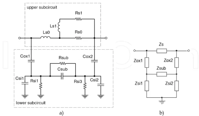
Fig. 1. The enhanced model of spiral inductor (a) and its schematic representation (b)
From the analysis point of view, the model can be represented using the equivalent schematic, shown in Fig. 1b (Durev et al., 2009). The following expressions can be written:
0 0 s s L sL Z ; Zs1Rs1sLs1; ZRs0 Rs0 ; 0 1 0 1 11 s R s s L s Z Z Z Z , (1) 2 1 2 1, 1 ox, ox sC Z ; ZRsi1,2 Rsi1,2; ZCsi1,2 1sCsi1,2 , (2) 2 1 2 1 2 1 1 11 , si C , si R , si Z Z Z
; ZRsub Rsub; ZCsub 1sCsub ;
sub C sub R sub Z Z Z 1 1 1 . (3)
The Y-parameters can be found using equations (1), (2) and (3). The corresponding schematics are shown in Fig. 2 for both cases – V2 0 (Fig. 2a) and V10 (Fig. 2b). According to the two-port definition for the Y-parameters, Y11 and Y21 are defined for the
case in Fig. 2a, and Y22 and Y12 – for the case, shown in Fig. 2b.
a) b) Fig. 2. Representation of the Y-parameter analysis: (a) V2 0; (b) V10 A method for optimal design and synthesis of CMOS inductors for use in RF circuits is
proposed in (Hershenson et al., 1999). The method is based on formulating the design problem as an optimization problem using geometric programming. The physical dimensions of the inductor are defined as design parameters. A variety of specifications are introduced including the required inductance value, as well as the minimum allowed values of the self-resonant frequency and the quality factor. Geometric constraints that can be handled include the maximum and the minimum values for each of the design parameters and a limit on total area.
The wide-band spiral inductor model, proposed in (Gil & Shin, 2003) is simple and has an excellent accuracy in comparison to the measured results. The main advantage of this model compared to the models with geometry dependent parameters developed in (Ashby et al., 1994; Yue et al. 1996; Mohan et al., 1999) consists in the frequency independence of the model parameters. Moreover, the models in (Ashby et al., 1994; Yue et al. 1996; Mohan et al., 1999) can not predict the drop-down characteristics in the series resistance at higher frequencies. The wide-band model was widely accepted and several extraction procedures were published to aid the verification and the easy implementation in the microelectronic designs (Kang et al., 2005; Chen et al., 2008). Several modifications of the model are proposed in (Sun et al., 2004 ; Wen & Sun, 2006). The application of the simple parameter extraction method (Kang et al., 2005) and the systematic model parameter extraction approach (Chen et al., 2008) lead to very accurate results. However, the application of these procedures takes time and the need of having automated extraction procedures using an industrial standard environment like MATLAB is an important problem to solve.
A bandwidth extension technique of gigahertz broadband circuitry is applied in (Mohan et al., 2000) by using optimized on-chip spiral inductors. A global optimization method, based on geometric programming, is discussed. As a result, the optimized on-chip inductors consume only 15% of the total area. A fast Sequential Quadratic Programming (SQP) approach to optimize the on-chip spiral inductors is proposed in (Zhan & Sapatnekar, 2004). A robust automated synthesis methodology to efficiently generate spiral inductor designs using multi-objective optimization techniques and surrogate functions to approximate Pareto surfaces in the design space is developed in (Nieuwoudt & Massoud, 2005). The obtained results indicate that the synthesis methodology efficiently optimizes inductor designs based on the defined requirements with an improvement of up to 51% in key inductor design constraints. The need to develop analysis and optimizations in one and the same environment leads to the usage of MATLAB and the implemented optimization toolboxes and GA toolbox (Chipperfield et al., 1994).
2. Wide-band planar inductor model analysis in MATLAB
The enhanced model of spiral inductor (Gil & Shin, 2003) can be treated as a parallel combination of an upper and a lower subcircuits (Fig. 1a). Because of the DC blocking property of the oxide capacitors Cox1 and Cox2, the spiral inductor model can be separated
into two parts: upper subcircuit and lower subcircuit. The inductor can be approximately characterized by the upper subcircuit for lower frequencies and by the lower subcircuit for high frequencies.
a) b)
Fig. 1. The enhanced model of spiral inductor (a) and its schematic representation (b)
From the analysis point of view, the model can be represented using the equivalent schematic, shown in Fig. 1b (Durev et al., 2009). The following expressions can be written:
0 0 s s L sL Z ; Zs1Rs1sLs1; ZRs0 Rs0 ; 0 1 0 1 11 s R s s L s Z Z Z Z , (1) 2 1 2 1, 1 ox, ox sC Z ; ZRsi1,2 Rsi1,2; ZCsi1,2 1sCsi1,2 , (2) 2 1 2 1 2 1 1 11 , si C , si R , si Z Z Z
; ZRsub Rsub; ZCsub 1sCsub ;
sub C sub R sub Z Z Z 1 1 1 . (3)
The Y-parameters can be found using equations (1), (2) and (3). The corresponding schematics are shown in Fig. 2 for both cases – V2 0 (Fig. 2a) and V10 (Fig. 2b). According to the two-port definition for the Y-parameters, Y11 and Y21 are defined for the
case in Fig. 2a, and Y22 and Y12 – for the case, shown in Fig. 2b.
a) b) Fig. 2. Representation of the Y-parameter analysis: (a) V2 0; (b) V10 A method for optimal design and synthesis of CMOS inductors for use in RF circuits is
proposed in (Hershenson et al., 1999). The method is based on formulating the design problem as an optimization problem using geometric programming. The physical dimensions of the inductor are defined as design parameters. A variety of specifications are introduced including the required inductance value, as well as the minimum allowed values of the self-resonant frequency and the quality factor. Geometric constraints that can be handled include the maximum and the minimum values for each of the design parameters and a limit on total area.
The wide-band spiral inductor model, proposed in (Gil & Shin, 2003) is simple and has an excellent accuracy in comparison to the measured results. The main advantage of this model compared to the models with geometry dependent parameters developed in (Ashby et al., 1994; Yue et al. 1996; Mohan et al., 1999) consists in the frequency independence of the model parameters. Moreover, the models in (Ashby et al., 1994; Yue et al. 1996; Mohan et al., 1999) can not predict the drop-down characteristics in the series resistance at higher frequencies. The wide-band model was widely accepted and several extraction procedures were published to aid the verification and the easy implementation in the microelectronic designs (Kang et al., 2005; Chen et al., 2008). Several modifications of the model are proposed in (Sun et al., 2004 ; Wen & Sun, 2006). The application of the simple parameter extraction method (Kang et al., 2005) and the systematic model parameter extraction approach (Chen et al., 2008) lead to very accurate results. However, the application of these procedures takes time and the need of having automated extraction procedures using an industrial standard environment like MATLAB is an important problem to solve.
A bandwidth extension technique of gigahertz broadband circuitry is applied in (Mohan et al., 2000) by using optimized on-chip spiral inductors. A global optimization method, based on geometric programming, is discussed. As a result, the optimized on-chip inductors consume only 15% of the total area. A fast Sequential Quadratic Programming (SQP) approach to optimize the on-chip spiral inductors is proposed in (Zhan & Sapatnekar, 2004). A robust automated synthesis methodology to efficiently generate spiral inductor designs using multi-objective optimization techniques and surrogate functions to approximate Pareto surfaces in the design space is developed in (Nieuwoudt & Massoud, 2005). The obtained results indicate that the synthesis methodology efficiently optimizes inductor designs based on the defined requirements with an improvement of up to 51% in key inductor design constraints. The need to develop analysis and optimizations in one and the same environment leads to the usage of MATLAB and the implemented optimization toolboxes and GA toolbox (Chipperfield et al., 1994).
2. Wide-band planar inductor model analysis in MATLAB
The enhanced model of spiral inductor (Gil & Shin, 2003) can be treated as a parallel combination of an upper and a lower subcircuits (Fig. 1a). Because of the DC blocking property of the oxide capacitors Cox1 and Cox2, the spiral inductor model can be separated
into two parts: upper subcircuit and lower subcircuit. The inductor can be approximately characterized by the upper subcircuit for lower frequencies and by the lower subcircuit for high frequencies.
3. Minimization the Parameter Extraction Errors Using GA
3.1. Purpose function and general structure
Once the basic circuit analysis and Y-parameter expressions are present, a GA approach can be applied to minimize the errors, coming from the parameter extraction procedure. The idea is to compare the Y-parameters, obtained for the model parameter values from the parameter extraction and the Y-parameters, obtained when the model parameter values are varied in a certain range. The actual comparison is done in the purpose function, which compares the absolute value for every frequency point of every two-port Y-parameter in one expression, using the sum of the least squares values:
n i i ) m ( jk i jk fun Y f Y f G 1 2 , (12) where j, k = 1,2; Yjk(m)– measured Y-parameters;Y – simulated Y-parameters of the model; jk
n – number of the measured/simulated frequency points.
The GA optimization is done using 1000 iterations, generation gap of 0.7 for population of 200 individuals. (Durev, 2009). The function body contains two for cycles. The first cycle runs the calculations for every frequency point until the end (DATA_ROWS), and the second cycle runs the calculations for every generated individual (variable) for a given frequency point until the end (Nind).
3.2. Optimization procedure realized in MATLAB
The representation of equations (1 - 11) and the construction of the optimization procedure in MATLAB are shown below:
for i = 1:DATA_ROWS %Calculate the frequency response of the circuit s = j*2*pi*frequency(i);
for ix = 1:Nind
ZLs0 = s.*Ls0(ix); Zs1 = Rs1(ix) + s.*Ls1(ix); ZRs0 = Rs0(ix); Zs = ZLs0 + ((Zs1.*ZRs0)./(Zs1 + ZRs0)); Zox1 = 1./(s.*Cox1(ix)); Zox2 = 1./(s.*Cox2(ix)); ZRsi1 = Rsi1(ix); ZCsi1 = 1./(s.*Csi1(ix));
Zsi1 = (ZRsi1.*ZCsi1)./(ZRsi1 + ZCsi1); ZRsi2 = Rsi2(ix); ZCsi2 = 1./(s.*Csi2(ix)); Zsi2 = (ZRsi2.*ZCsi2)./(ZRsi2 + ZCsi2); ZRsub = Rsub(ix); ZCsub = 1./(s.*Csub(ix)); Zsub = (ZRsub.*ZCsub)./(ZRsub + ZCsub);
%Calculate Y11, V1 = 1, V2 = 0
Zox2si2 = (Zox2.*Zsi2)./(Zox2 + Zsi2); Zsubox2si2 = Zox2si2 + Zsub; Zsubox2si2si1 = (Zsi1.*Zsubox2si2)./(Zsi1 + Zsubox2si2);
Zsubox2si2si1ox1 = Zox1 + Zsubox2si2si1;
ZeqY11 = (Zs.*Zsubox2si2si1ox1)./(Zs + Zsubox2si2si1ox1); Y11(ix, 1) = V1./ZeqY11;
%Calculate Y22, V1 = 0, V2 = 1
Zox1si1 = (Zox1.*Zsi1)./(Zox1 + Zsi1); Zsubox1si1 = Zox1si1 + Zsub; Zsubox1si1si2 = (Zsi2.*Zsubox1si1)./(Zsi2 + Zsubox1si1);
Zsubox1si1si2ox2 = Zox2 + Zsubox1si1si2;
ZeqY22 = (Zs.*Zsubox1si1si2ox2)./(Zs + Zsubox1si1si2ox2); The equivalent impedance ZeqY11 for the schematic, shown in Fig. 2a can be found, using the
following equations: 2 2 2 2 1 11 si ox si ox Z Z Z ; Zsubox2si2 Zox2si2Zsub ; 2 2 1 1 2 2 1 11 si subox si si si subox Z Z Z , (4) Zsubox2si2si1ox1Zox1Zsubox2si2si1; 1 1 2 2 11 1 1 1 ox si si subox s eqY Z Z Z . (5)
The following expression for Y11 can be written:
11 1
11 V ZeqY
Y . (6)
The equivalent impedance ZeqY22 and Y22 are obtained similarly from the analysis of the
schematic in Fig. 2b, when V10. The following expressions are valid:
2 2 1 1 22 1 1 1 ox si si subox s eqY Z Z Z ; Y22 V2 ZeqY22 . (7)
Y21 can be easily expressed if the voltage VZox2across Zox2 in Fig. 2a is known. It can be
symbolically expressed using the symbolic analysis possibilities in MATLAB. If the input current, node voltages and admittances in Fig. 2 are declared as symbols using syms, the Modified Nodal Analysis (MNA) circuit matrix equation can be solved and the following expression can be written for VZox2:
1 1
12 21
2 2
2 si ox sub si ox sub si ox sub ox ox Z Y Y .Y YY .YYV Y . Y Y V . (8)In order to obtain Y21, the currents IZox2 and Is are expressed, using the following
equations: 2 2 2 Zox ox ox Z V Z I ; Is V1 Zs . (9)
Using the expressions (9) and the Y21 two-port definition, Y21 is expressed in the form:
2
121 I I V
Y sZox . (10)
Because of the symmetry of the model from Fig. 1b, the following expression is obtained for Y12 from the analysis of the circuit, shown in Fig. 2b when V10:
1
212 I I V
The corresponding relative errors are: RelErrY11max = 0.254 %, RelErrY12max = 0.062 %,
RelErrY21max = 0.062 %, RelErrY22max = 0.239 %. After the GA optimization, the following
model parameter values are obtained: Rs0 = 6.697 Ω, Rs1 = 7.558 Ω, Ls0 = 3.02 nH,
Ls1 = 1.184 nH, Cox1 = 119.776 fF, Cox2 = 112.479 fF, Rsi1 = 292.638 Ω, Rsi2 = 285.733 Ω,
Csi1 = 33.997 fF, Csi2 = 32.958 fF, Rsub = 944.4 Ω and Csub = 72.516 fF.
The corresponding relative errors after the GA optimization are: RelErrY11max = 0.099 %,
RelErrY12max = 0.041 %, RelErrY21max = 0.041 %, RelErrY22max = 0.154 %. Thus the improvement
of the errors is 61%, 34%, 34% and 36% respectively. The improvement is achieved with 0.5% variation of the model parameter values. The proposed algorithm shows excellent agreement with the measured data over the whole frequency range.
4. Parameter extraction of the
wide-band planar inductor model using MATLAB
Several extraction procedures for wide-band on-chip spiral inductor model are proposed in (Kang et al., 2005; Chen et al., 2008). An automated parameter extraction procedure using MATLAB is developed in (Gadjeva et al., 2009).
The input data is supplied to the MATLAB script as an Excel file .xls. The data is structured in columns, starting from the frequency column, followed by the real and imaginary parts of the measured two-port S-parameters: S11re, S11im, S12re, S12im, S21re, S21im, S22re and S22im.
The program has the option for the two-port Y-parameters to be the input data. In the most cases the input data are the measured S-parameters, which are easier to measure and the network analyzers provide this data. Once accepted from the .xls file, the S-parameters are converted to Y-parameters, as the parameter extraction procedure works with Y-parameters. The conversion is done using the MATLAB s2y function. Once converted, the input data is structured into five vectors: [freq]n1, [Y11]n1, [Y12]n1, [Y21]n1, [Y22]n1, where n is the number of points, measured as input data. The input data can be represented as a matrix [INPUT_DATA]DATA_ROWS x 9 for nine input data vectors – frequency vector matrix and the
real and the imaginary parts vectors for the two-port S- or Y-parameters.
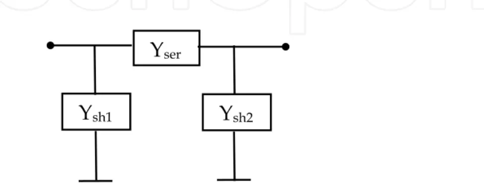
The enhanced model of spiral inductor (Gil & Shin, 2003) shown in Fig. 1a can be approximately characterized by the upper subcircuit for lower frequencies. Such an approximation has been widely applied to calculate the series resistance and inductance (Kang et al., 2005; Huang et al., 2006). To minimize the error, caused by the approximation, the upper frequency limit must be calculated and fixed in the parameter extraction program. For this reason, the spiral inductor model shown in Fig. 1a can be represented by the equivalent schematics in Fig. 3 (π-network).
Fig. 3. Relation between the shunt and series admittances of the π-network for the spiral inductor model
Y
serY
sh2Y
sh1Y22(ix, 1) = U2./ZeqY22;
Ysub = 1./Zsub; Yox1 = 1./Zox1; Yox2 = 1./Zox2; Ysi1 = 1./Zsi1; Ysi2 = 1./Zsi2; %Calculate Y12, V1 = 0, V2 = 1
%Expressions taken from symmetry considerations with Y21
VZox1 = (Yox2.*Ysub)./((Yox2 + Ysi2).*(Ysub + Yox1 + Ysi1) + Ysub.*(Yox1 + Ysi1)); IZox1 = VZox1./Zox1; Is = V2./Zs; I1 = Is + IZox1; Y12(ix, 1) = -I1./U2;
%Calculate Y21, V1 = 1, V2 = 0
%Expressions taken from the symbolic extraction of Y21
VZox2 = (Yox1.*Ysub)./((Yox1 + Ysi1).*(Ysub + Yox2 + Ysi2) + Ysub.*(Yox2 + Ysi2)); IZox2 = VZox2./Zox2; Is = V1./Zs; I2 = Is + IZox2;
Y21(ix, 1) = -I2./U1; end
%Least squares sum of the difference between the modules of the required and the current Y-parameters
g_fun = g_fun + ((abs(Y11) - abs(Y11_req(i)))).^2 + ((abs(Y12) - abs(Y12_req(i)))).^2 + ((abs(Y21) - abs(Y21_req(i)))).^2 + ((abs(Y22) - abs(Y22_req(i)))).^2;
end
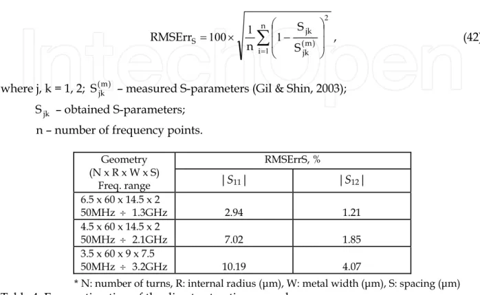
The presented procedure for optimization of the model parameters of the wide-band on-chip spiral inductor model is verified according to the published data in (Gil & Shin, 2003; Chen et al., 2008). The relative percentage error for the modules of the extracted and the measured Y-parameters is used to estimate the accuracy of the optimization procedure for various geometry RF spiral inductors. The maximal relative percentage error is calculated for the modules of the Y-parameters in the form:
i ) m ( jk i jk i max Y f Y f Y max . lErr Re 100 1 , (13) where j, k = 1,2; (m) jk Y - measured Y-parameters;Y - simulated Y-parameters of the model. jk
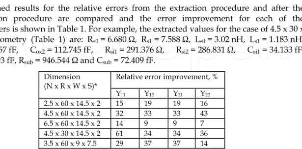
The obtained results for the relative errors from the extraction procedure and after the optimization procedure are compared and the error improvement for each of the Y-parameters is shown in Table 1. For example, the extracted values for the case of 4.5 x 30 x 14.5 x 2 geometry (Table 1) are: Rs0 = 6.680 Ω, Rs1 = 7.588 Ω, Ls0 = 3.02 nH, Ls1 = 1.183 nH,
Cox1 = 119.57 fF, Cox2 = 112.745 fF, Rsi1 = 291.376 Ω, Rsi2 = 286.831 Ω, Csi1 = 34.133 fF,
Csi2 = 32.993 fF, Rsub = 946.544 Ω and Csub = 72.409 fF. Dimension
(N x R x W x S)* Relative error improvement, %
Y11 Y12 Y21 Y22 2.5 x 60 x 14.5 x 2 15 19 19 16 4.5 x 60 x 14.5 x 2 32 33 33 43 6.5 x 60 x 14.5 x 2 14 9 9 7 4.5 x 30 x 14.5 x 2 61 34 34 36 3.5 x 60 x 9 x 7.5 29 37 37 14
* N: number of turns, R: inner radius (μm), W: metal width (μm), S: spacing (μm)
The corresponding relative errors are: RelErrY11max = 0.254 %, RelErrY12max = 0.062 %,
RelErrY21max = 0.062 %, RelErrY22max = 0.239 %. After the GA optimization, the following
model parameter values are obtained: Rs0 = 6.697 Ω, Rs1 = 7.558 Ω, Ls0 = 3.02 nH,
Ls1 = 1.184 nH, Cox1 = 119.776 fF, Cox2 = 112.479 fF, Rsi1 = 292.638 Ω, Rsi2 = 285.733 Ω,
Csi1 = 33.997 fF, Csi2 = 32.958 fF, Rsub = 944.4 Ω and Csub = 72.516 fF.
The corresponding relative errors after the GA optimization are: RelErrY11max = 0.099 %,
RelErrY12max = 0.041 %, RelErrY21max = 0.041 %, RelErrY22max = 0.154 %. Thus the improvement
of the errors is 61%, 34%, 34% and 36% respectively. The improvement is achieved with 0.5% variation of the model parameter values. The proposed algorithm shows excellent agreement with the measured data over the whole frequency range.
4. Parameter extraction of the
wide-band planar inductor model using MATLAB
Several extraction procedures for wide-band on-chip spiral inductor model are proposed in (Kang et al., 2005; Chen et al., 2008). An automated parameter extraction procedure using MATLAB is developed in (Gadjeva et al., 2009).
The input data is supplied to the MATLAB script as an Excel file .xls. The data is structured in columns, starting from the frequency column, followed by the real and imaginary parts of the measured two-port S-parameters: S11re, S11im, S12re, S12im, S21re, S21im, S22re and S22im.
The program has the option for the two-port Y-parameters to be the input data. In the most cases the input data are the measured S-parameters, which are easier to measure and the network analyzers provide this data. Once accepted from the .xls file, the S-parameters are converted to Y-parameters, as the parameter extraction procedure works with Y-parameters. The conversion is done using the MATLAB s2y function. Once converted, the input data is structured into five vectors: [freq]n1, [Y11]n1, [Y12]n1, [Y21]n1, [Y22]n1, where n is the number of points, measured as input data. The input data can be represented as a matrix [INPUT_DATA]DATA_ROWS x 9 for nine input data vectors – frequency vector matrix and the
real and the imaginary parts vectors for the two-port S- or Y-parameters.
The enhanced model of spiral inductor (Gil & Shin, 2003) shown in Fig. 1a can be approximately characterized by the upper subcircuit for lower frequencies. Such an approximation has been widely applied to calculate the series resistance and inductance (Kang et al., 2005; Huang et al., 2006). To minimize the error, caused by the approximation, the upper frequency limit must be calculated and fixed in the parameter extraction program. For this reason, the spiral inductor model shown in Fig. 1a can be represented by the equivalent schematics in Fig. 3 (π-network).
Fig. 3. Relation between the shunt and series admittances of the π-network for the spiral inductor model
Y
serY
sh2Y
sh1Y22(ix, 1) = U2./ZeqY22;
Ysub = 1./Zsub; Yox1 = 1./Zox1; Yox2 = 1./Zox2; Ysi1 = 1./Zsi1; Ysi2 = 1./Zsi2; %Calculate Y12, V1 = 0, V2 = 1
%Expressions taken from symmetry considerations with Y21
VZox1 = (Yox2.*Ysub)./((Yox2 + Ysi2).*(Ysub + Yox1 + Ysi1) + Ysub.*(Yox1 + Ysi1)); IZox1 = VZox1./Zox1; Is = V2./Zs; I1 = Is + IZox1; Y12(ix, 1) = -I1./U2;
%Calculate Y21, V1 = 1, V2 = 0
%Expressions taken from the symbolic extraction of Y21
VZox2 = (Yox1.*Ysub)./((Yox1 + Ysi1).*(Ysub + Yox2 + Ysi2) + Ysub.*(Yox2 + Ysi2)); IZox2 = VZox2./Zox2; Is = V1./Zs; I2 = Is + IZox2;
Y21(ix, 1) = -I2./U1; end
%Least squares sum of the difference between the modules of the required and the current Y-parameters
g_fun = g_fun + ((abs(Y11) - abs(Y11_req(i)))).^2 + ((abs(Y12) - abs(Y12_req(i)))).^2 + ((abs(Y21) - abs(Y21_req(i)))).^2 + ((abs(Y22) - abs(Y22_req(i)))).^2;
end
The presented procedure for optimization of the model parameters of the wide-band on-chip spiral inductor model is verified according to the published data in (Gil & Shin, 2003; Chen et al., 2008). The relative percentage error for the modules of the extracted and the measured Y-parameters is used to estimate the accuracy of the optimization procedure for various geometry RF spiral inductors. The maximal relative percentage error is calculated for the modules of the Y-parameters in the form:
i ) m ( jk i jk i max Y f Y f Y max . lErr Re 100 1 , (13) where j, k = 1,2; (m) jk Y - measured Y-parameters;Y - simulated Y-parameters of the model. jk
The obtained results for the relative errors from the extraction procedure and after the optimization procedure are compared and the error improvement for each of the Y-parameters is shown in Table 1. For example, the extracted values for the case of 4.5 x 30 x 14.5 x 2 geometry (Table 1) are: Rs0 = 6.680 Ω, Rs1 = 7.588 Ω, Ls0 = 3.02 nH, Ls1 = 1.183 nH,
Cox1 = 119.57 fF, Cox2 = 112.745 fF, Rsi1 = 291.376 Ω, Rsi2 = 286.831 Ω, Csi1 = 34.133 fF,
Csi2 = 32.993 fF, Rsub = 946.544 Ω and Csub = 72.409 fF. Dimension
(N x R x W x S)* Relative error improvement, %
Y11 Y12 Y21 Y22 2.5 x 60 x 14.5 x 2 15 19 19 16 4.5 x 60 x 14.5 x 2 32 33 33 43 6.5 x 60 x 14.5 x 2 14 9 9 7 4.5 x 30 x 14.5 x 2 61 34 34 36 3.5 x 60 x 9 x 7.5 29 37 37 14
* N: number of turns, R: inner radius (μm), W: metal width (μm), S: spacing (μm)
The frequency range, where the upper subcircuit from Fig. 1a represents the approximate behaviour of the spiral inductor model, is then fixed to [Fmin; F1], where F1 is the minimal
value of the frequencies freq_low_rat1u and freq_low_rat2u.
Once F1 and Fmax were calculated, the low and high frequency vectors:
[freq_low]freq_low_rows x freq_low_columns and [freq_high]freq_high_rows x
freq_high_columns can be found, which will be needed for the further indexing of the matrices in the calculations:
for i = 1:DATA_ROWS if(freq(i) <= F1) freq_low(i, 1) = freq(i); elseif(freq(i) <= Fmax) freq_high(i, 1) = freq(i); end end
[freq_low_rows, freq_low_columns] = size(freq_low); [freq_high_rows, freq_high_columns] = size(freq_high);
4.1. Extraction of Ls0, Rs0, Ls1, and Rs1
The equivalent resistance and inductance of the upper subcircuit are obtained for the frequency range [Fmin ; F1]:
] Z [ Ruf u ; [Z ] L u uf ; Zu 1Y12 . (16)
The dc resistance and inductance Rdc and Ldc are calculated for ω = 0. In the real case these
values are calculated for 2Fminaccording to the following expressions:
i min f u i max dc f F R max R i ;
i f u i max dc maxL L . (17)The relation between the differences ΔRuf and ΔLuf gives the coefficient T from (Chen et al.,
2008) defined in the form:
max dc uf uf R R R ; Luf Ldcmax Luf, (18) uf uf L R T ; i i uf uf i i max L R . F f max T 1 . (19)
The coefficient M and its maximal value Mmax are obtained in the form (Chen et al., 2008):
1 2
R T M uf ; Mmax maxi
Rufi
1T2i
; TT . (20)The values of Rs0, Rs1, Ls0 and Ls1 are calculated directly from the obtained scalar values for
Rdcmax, Ldcmax, Tmax and Mmax (Chen et al. , 2008): max dc max s M R R 0 ; max max dc s s R MR R 0 1 , (21)
In this network, the following expressions are valid (Chen et al., 2008): 12 Y Yser ; Ysh1Y11Y12; Ysh2Y22Y12, (14) ser sh u YY RAT 1 1 100 ; ser sh u YY RAT 2 2 100 . (15)
It is shown in (Chen et al., 2008) that the normalized magnitudes of the upper subcircuit
u
RAT1 and RAT2u should be smaller than 1% in order to achieve accurate low frequency approximation. The frequency values in the [freq]n1data vector are in the range
[Fmin; Fmax]. Fmin is the start frequency and Fmax is the end frequency at which the input
two-port Y- or S-parameters are measured. The values of these two frequencies can be easily defined in MATLAB using min and max functions over the vector [freq]n1:
Fmin = min(freq); Fmax = max(freq);
The expressions (14) and (15), written as a MATLAB code are in the form: Ysh1 = Y11 + Y12; Ysh2 = Y22 + Y12;
rat1u = 100*abs(Ysh1./Y12); rat2u = 100*abs(Ysh2./Y12);
The maximal frequencies, at which the normalized magnitudes of the vector components are less than 1%, can be found using the following code over the matrices [freq]n1, [RAT1u]n1 and [RAT2u]n1 : for i = 1:DATA_ROWS if(rat1u(i) <= 1.0) freq_low_rat1u = freq(i); elseif(rat1u_min > 1.0) freq_low_rat1u = freq_low_rat1u_min; ErrorMsg end if(rat2u(i) <= 1.0) freq_low_rat2u = freq(i); elseif(rat2u_min > 1.0) freq_low_rat2u = freq_low_rat2u_min; ErrorMsg end end F1 = min(freq_low_rat1u, freq_low_rat2u);
Here n = DATA_ROWS and an error message ErrorMsg is written in case when there are no component values in [RAT1u]n1 and [RAT2u]n1, smaller than 1%. This occurs when the input data have not enough number of points or they are not precisely measured. The minimum values found in vectors [RAT1u]n1 and [RAT2u]n1(freq_low_rat1u_min and freq_low_rat2u_min) are taken into account in this case and this could cause deviations in the calculations.
The expressions (23) – (27), written as a MATLAB code, are in the form:
Zs = j*w*Ls0 + (1./((1/Rs0) + (1./(Rs1 + j*w*Ls1)))); Ys = 1./Zs; Y11l = Y11 - Ys;
Y12l = Y12 + Ys; Y22l = Y22 - Ys; Ysh1l = Y11l + Y12l; Ysh2l = Y22l + Y12l; Yserl = -Y12l; rat1l = 100.*abs(Yserl./Ysh1l); rat2l = 100.*abs(Yserl./Ysh2l);
The maximal frequencies, at which the components of the vector of normalized magnitudes have values less than 5%, can be found using the following code over the matrices
1
n
] frequency
[ , [RAT1l]n1 and [RAT2l]n1: for i = 1:DATA_ROWS if(freq(i) >= F1) if(rat1l(i) <= 5.0) freq_low_rat1l = freq(i); elseif(rat1l_min > 5.0) freq_low_rat1l = freq_low_rat1l_min; ErrorMsg end if(rat2l(i) <= 5.0) freq_low_rat2l = freq(i); elseif(rat2l_min > 5.0) freq_low_rat2l = freq_low_rat2l_min; ErrorMsg end end end F2 = min(freq_low_rat1l, freq_low_rat2l);
ErrorMsg is written in case there are no component values in [RAT1l]n1 and [RAT2l]n1, smaller than 5%. The minimum values found in vectors [RAT1l]n1 and [RAT2l]n1 namely freq_low_rat1l_min and freq_low_rat2l_min are taken into account in this case and this could cause deviations in the calculations.
The frequency range, where the lower subcircuit from Fig. 1a represents the approximate behaviour of the spiral inductor model is then fixed to [F1; F2], where F2 is the minimal
frequency between freq_low_rat1l and freq_low_rat2l.
Once F2 is calculated, the middle frequency vector [freq_mid]freq_mid_rows x freq_mid_columns can be
found, which will be needed for the further indexing of the matrices in the calculations: for i = 1:DATA_ROWS
if(freq(i) <= F2)
freq_mid(i, 1) = freq(i); end
end
[freq_mid_rows, freq_mid_columns] = size(freq_mid);
Then Cox1 and Cox2 can be extracted as maximal values in the range [F1; F2] using the
expressions from (Chen et al., 2008):
l l
ox Y Y C 12 11 1 1 1 ;
l l ox Y Y C 12 22 2 1 1 . (28) max max max dc s L M T L 0 ; max s s s R T R L 0 1 1 . (22)Using the equations (16) – (21), the upper subcircuit parameter extraction can be done with the following MATLAB source code:
Zu = -1./Y12; Ruf = real(Zu([1 : freq_low_rows], 1)); Rdc = (Ruf*Fmin)./freq_low; Luf = imag(Zu([1 : freq_low_rows], 1))./(w([1 : freq_low_rows], 1));
Rdc_max = max(Rdc) + 1.0e-15; Ldc_max = max(Luf) + 1.0e-15; DRuf = Ruf - Rdc_max; DLuf = Ldc_max - Luf;
T = ((freq_low./F1).*DRuf)./DLuf; %Luf(x,x) = Ldc_max => Warning: Divide by zero. T_max = max(T); Tw = T_max./w([1 : freq_low_rows], 1);
M = DRuf.*(1 + (Tw.*Tw)); M_max = max(M); Rs0 = M_max + Rdc_max;
Rs1 = (Rs0*Rdc_max)/M_max; Rt = Rs0 + Rs1; Ls0 = Ldc_max - (M_max/T_max); Ls1 = (Rs0+Rs1)/T_max;
A small number of 11015 is added to calculate R
dcmax and Ldcmax to avoid division by zero. 4.2. Extraction of Cox1 and Cox2
Once the model parameters Rs0, Rs1, Ls0 and Ls1 are calculated, based on measured data in
the frequency range [Fmin, F1], the equivalent series impedance Zs and admittance Ys of the
upper subcircuit can be found using the following expressions:
1 1 0 0 1 1 1 s s s s s L j R R L j Z ; s s Z Y 1 . (23)
For frequencies greater than F1 the lower subcircuit has to be taken into account. The
Y-matrix of the lower subcircuit [Yl] is obtained in the form:
Yl
Y
Ys , (24)where [Ys] is the admittance matrix of the upper subcircuit;
[Y] - admittance matrix of the entire model.
s l Y Y
Y11 11 ; Y12l Y12Ys ; Y22l Y22 Ys. (25) The lower subcircuit from Fig. 1a can be represented again as a π-network. The following expressions are valid for this subcircuit (Chen et al., 2008):
l l l sh Y Y Y 1 11 12 ; Ysh2l Y22l Y12l ; Yserl Y12l, (26) l sh l ser l Y Y RAT 1 1 100 ; l sh l ser l Y Y RAT 2 2 100 . (27)
It is shown in (Chen et al., 2008) that the normalized magnitudes of the lower subcircuit
l
RAT1 and RAT2l should be smaller than 5% in order to achieve accurate high frequency
Csi2 = max((freq([freq_mid_rows : freq_high_rows], 1)/Fmax).*imag(DV2([freq_mid_rows : freq_high_rows], 1)./DV([freq_mid_rows : freq_high_rows], 1))./w([freq_mid_rows : freq_high_rows], 1));
The following expression for the admittance Ysub can be used to extract Rsub and Csub:
1 2 1
2 2 a a ox V V sub V /V j C Y ; (35)
1 i max sub i sub max f F Y R ;
i sub i sub max Y C . (36)Expressions (35) and (36) are represented in MATLAB using the following code over matrix operations:
Ysub = ((DV2./DV) + j*w*Cox2)./((V1a./V2a) - 1);
Rsub = 1/max((freq([freq_mid_rows : freq_high_rows], 1)/Fmax).* real(Ysub([freq_mid_rows : freq_high_rows], 1)));
Csub = max(imag(Ysub([freq_mid_rows : freq_high_rows], 1))./w([freq_mid_rows : freq_high_rows], 1));
4.4. Results of the extraction procedure of the wide-band inductor model
The presented procedure for parameter extraction of wide-band on-chip spiral inductor model in MATLAB was verified according to the published data in (Gil & Shin, 2003). The relative error over the frequency range for the real and the imaginary part of the measured and the extracted Y-parameters is used to estimate the accuracy of the extraction procedure for various geometry RF spiral inductors. The maximal relative error is calculated over the modules of the Y-parameters, using formula (13). The obtained results are presented in Table 2. They are in agreement with the measured results from (Gil & Shin, 2003; Chen et al., 2008). The maximal relative error is less than 0.5% which makes the parameter on-chip spiral inductor parameter extraction procedure very accurate. For example the extracted values for the case of 4.5 x 30 x 14.5 x 2 geometry (Table 2) are: Rs0 = 6.681 Ω, Rs1 = 7.589 Ω,
Ls0 = 3.02 nH, Ls1 = 1.183 nH, Cox1 = 119.571 fF, Cox2 = 112.745 fF, Rsi1 = 291.377 Ω, Rsi2 =
286.832 Ω, Csi1 = 34.134 fF, Csi2 = 32.994 fF, Rsub = 946.544 Ω and Csub = 72.41 fF. Dimension (N x R x W x S) Y RelErrY, % 11 Y12 Y21 Y22 2.5 x 60 x 14.5 x 2 0.173 0.054 0.054 0.164 4.5 x 60 x 14.5 x 2 0.451 0.101 0.101 0.391 6.5 x 60 x 14.5 x 2 0.479 0.151 0.151 0.436 4.5 x 30 x 14.5 x 2 0.254 0.062 0.062 0.239 3.5 x 60 x 9 x 7.5 0.235 0.065 0.065 0.216
* N: number of turns, R: inner radius (μm), W: metal width (μm), S: spacing (μm)
Table 2. Error estimation of the extraction procedure The following MATLAB source code is used for the calculation of Cox1 and Cox2:
Cox1 = max(-1./(imag(1./(Y11l([freq_low_rows : freq_mid_rows], 1) + Y12l([freq_low_rows : freq_mid_rows], 1))).*w([freq_low_rows : freq_mid_rows], 1)));
Cox2 = max(-1./(imag(1./(Y22l([freq_low_rows : freq_mid_rows], 1) + Y12l([freq_low_rows : freq_mid_rows], 1))).*w([freq_low_rows : freq_mid_rows], 1)));
4.3. Extraction of Rsi1, Rsi2, Csi1, Csi2, Rsub and Csub
The lower subcircuit represents the behavior of the model in the range [F2; Fmax]. It is
analyzed for the extraction of Rsi1, Rsi2, Csi1, Csi2, Rsub and Csub based on the relations between
the lower subcircuit Y-parameters and the input and output voltages V1and V2using the previously extracted values for the model parameters Cox1 and Cox2 .
1 11 1 1 j YC V V 1 ox l a ; 12 1 2 j YC V V 2 ox l a , (29) 2 2 22 2 1 j YC V V ox l b ; V1 j YC12 V2 1 ox l b , (30) a b a a V V1 V2 V1 V2 ; V1
Y11 Y12
V2b
Y22 Y12
V2a, (31)
a
b V2 Y22 Y12 V1 Y11 Y12 V1 . (32)As a result, the model parameters Rsi1, Rsi2, Csi1, Csi2 can be extracted directly as follows:
V V max i i si max f F R 1 1 ;
V V max i i si max f F R 2 2 , (33)
i V V max i i si max (f F ) C 1 1 ;
i V V max i i si max (f F ) C 2 2 . (34)Expressions (29) – (34) are represented in MATLAB using the following code over matrices operations:
Zcox1 = 1./(j*w*Cox1); Zcox2 = 1./(j*w*Cox2); V1a = 1 - (Y11l.*Zcox1); V2a = -(Y12l.*Zcox2); V2b = 1 - (Y22l.*Zcox2); V1b = -(Y12l.*Zcox1); DV = (V1a.*V2b) - (V1b.*V2a);
DV1 = ((Y11 + Y12).*V2b) - ((Y22 + Y12).*V2a); DV2 = (V1a.*(Y22 + Y12)) - (V1b.*(Y11 + Y12));
Rsi1 = max((freq([freq_mid_rows : freq_high_rows], 1)/Fmax)./real(DV1([freq_mid_rows : freq_high_rows], 1)./DV([freq_mid_rows : freq_high_rows], 1)));
Rsi2 = max((freq([freq_mid_rows : freq_high_rows], 1)/Fmax)./real(DV2([freq_mid_rows : freq_high_rows], 1)./DV([freq_mid_rows : freq_high_rows], 1)));
Csi1 = max((freq([freq_mid_rows : freq_high_rows], 1)/Fmax).*imag(DV1([freq_mid_rows : freq_high_rows], 1)./DV([freq_mid_rows : freq_high_rows], 1))./w([freq_mid_rows : freq_high_rows], 1));
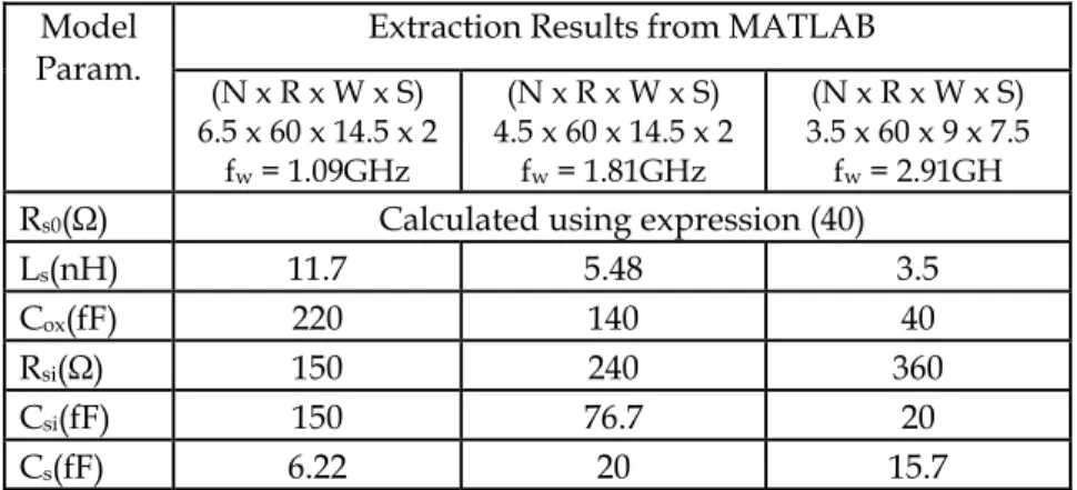
The parameters Rs , Ls , Rsi and Cox are obtained for lower frequencies (f = fl). The parameter
Csi is determined for high frequencies (f = fh):
l s Z R 3 ; Ls
Z3l l ; Rsi
Z1l , (37)
l l ox Z C 1 1 ;
ox h si C Z C 1 1 1 . (38)The series resistance Rsw is obtained for the working frequency fw. Cs is obtained for the
resonant frequency:
w s
w
sw L Y R 2 3 ;
2 2 0 s sw s s L L R C . (39)The series resistance Rs in Fig. 4 is frequency dependent. If the geometry of the extracted
spiral inductor is known, Rs can be calculated using the formula (Yue et al., 1996):
t s w l e R 1 , (40)where w is the width of the metal strips, δ is the skin-effect depth into the metal layers, σ is the conductivity of metal layers, l is the length of the spiral, t is the thickness of the metal layer of the spiral (Yue et al., 1996). In case when the geometry of the spiral inductor is not known, Rs can be calculated using the formula (Ashby et al., 1994):
2
1
01 K
s R K f
R , (41)
where the coefficients K1 and K2 determine the frequency dependence of Rs.
The model parameters results after the application of the described direct extraction procedure are given in Table 3.
Model
Param. Extraction Results
(N x R x W x S) 6.5 x 60 x 14.5 x 2 fw = 1.09GHz (N x R x W x S) 4.5 x 60 x 14.5 x 2 fw = 1.81GHz (N x R x W x S) 3.5 x 60 x 9 x 7.5 fw = 2.91GHz Rs0(Ω) 7.6 5.06 5.68 Rsw(Ω) 9.08 6.351 5.7 Ls(nH) 11.9 5.67 3.56 Cox(fF) 232.92 157.02 86.78 Rsi(Ω) 138.62 225.48 340.28 Csi(fF) 123.59 79.98 67.58 Cs(fF) 45.76 96.04 152.99
* N: number of turns, R: internal radius (μm), W: metal width (μm), S: spacing (μm)
Table 3. Model parameter values after the application of the direct extraction procedure
5. Parameter Extraction of Physical Geometry
Dependent RF Planar Inductor Model
The physical model of planar spiral inductor on silicon (Yue et al., 1996) is a very popular model used in microelectronic design. Its model parameter values can be expressed directly using the geometry of the spiral inductor. The skin effect at high frequencies is modeled using a frequency dependent series resistance. Several extraction procedures are developed for the physical spiral inductor model – direct procedures (Shih et al., 1992), optimization based procedures (Post, 2000). A number of approaches to geometry optimization of spiral inductors are proposed based on geometric programming optimization (Wenhuan & Bandler, 2006), parametric analysis (Hristov et al., 2003), etc. An approach is developed in (Durev et al., 2010) to direct parameter extraction based on the measured S-parameters. The approach gives excellent results for frequencies around the working frequency. GA based approach is used to refine the simulated S-parameters and to minimize the post extraction errors for the full investigated frequency range.
5.1. Analysis of the spiral inductor model
The physical model of spiral inductor (Yue et al., 1996) is shown in Fig. 4. The model parameters are Rs, Rsi, Cs, Cox, Csi and Ls. The series resistance takes into account the skin depth
of the conductor. Ls is the inductance of the spiral, Cox represents the capacitance between the
spiral and the substrate. Rsi and Csi model the resistance and the capacitance of the substrate,
and Cs models the parallel-plate capacitance between the spiral and the center-tap underpass.
The presented extraction procedure is based on the measured two-port S-parameters.
Fig. 4. Physical model of spiral inductor
As the model parameters can be easily expressed by the two-port Y-parameters, the measured S-parameters Sijm are converted to Y-parameters Yijm, i, j = 1, 2. The parameter
extraction procedure is based on determination of the admittances Y1, Y2 and Y3 (Fig. 4) as a
function of the two-port Y-parameters. The next step is to express the admittances Y1 and Y3