How to cite this paper: Rahman, M.K., Musa, A.M.M., Neher, B., Patwary, K.A., Rahman, M.A. and Islam,M.S. (2016) A Re-view of the Study on the Electromigration and Power Electronics. Journal of Electronics Cooling and Thermal Control, 6, 19-31. http://dx.doi.org/10.4236/jectc.2016.61002
Electromigration and Power Electronics
Md. Khalilur Rahman1*, Abul Monsur Mohammed Musa2, Budrun Neher1,Kawchar Ahmed Patwary1, Mohammad Atiqur Rahman3, Md. Shariful Islam4 1Department of Physics, Comilla University, Comilla, Bangladesh
2Department of Physics, University of Chittagong, Chittagong, Bangladesh 3Department of Chemistry, Comilla University, Comilla, Bangladesh 4Department of ICT, Comilla University, Comilla, Bangladesh
Received 15 November 2015; accepted 27 March 2016; published 30 March 2016
Copyright © 2016 by authors and Scientific Research Publishing Inc.
This work is licensed under the Creative Commons Attribution International License (CC BY). http://creativecommons.org/licenses/by/4.0/
Abstract
Electromigration is a main challenge in the pursuit of power electronics, because physical limit to increase current density in power electronics is electromigration (EM), whereas much higher electrical current and voltage are required for power electronics packaging. So the effect of EM is an important issue in applications where high current densities are used, such as in microelec-tronics and related structures (e.g., Power ICs). Since the structure size of integrated circuits (ICs) decreases and the practical significance of this effect increases, the result is EM failure. On the other hand, in the next generation power electronics technology electrical current density is ex-pected to exceed 107 A/cm2 which is another challenge. This review work has been carried out to
identify the mechanism of EM damage in power electronics (e.g., pure metallization and solder joints) and also how to control this kind of damage.
Keywords
Voids and Hillocks, Interconnect, Solder Joint, Thermomigration, MTF, Reliability of IC
1. Introduction
can cause the eventual loss of connections or failure of a circuit [7]. Whereas the reliability of interconnect un-der high electrical stressing is essential for high power electronics packaging. So it is an important issue for economic and human safety, and survival reasons.
EM is the phenomenon of interconnect metal by self-diffusion along an interconnection as high current den-sity is passing through the interconnect [8] [9] in Figure 1, which is nothing but the “transport of material due to the gradual movement of the ions in a conductor by simple momentum transfer between conducting electrons and diffusing metal atoms” [10]. So EM occurs within a metal conductor when large numbers of high-speed current carrying electrons impact on metal lattice and dislodge atoms by simple momentum exchange shown in Figure 2 [3] [11].
As a result voids will be formed on some parts of the interconnection [14] and hillock due to the accumulation of the metal atoms will be formed on different parts of the interconnection [5]. The presence of voids will in-crease the resistance [15] [16] of the interconnection or even open, while inin-creased mechanical stress may result in dielectric fractures and leakage between adjacent interconnects in Figure 3and Figure 4. On the other hand, the presence of hillock will cause short circuit between the adjacent interconnections if the hillock is developed side-way, and short circuit between the different levels of interconnections if it is developed vertically and punch through the inter-metal dielectric. Finally, the function of the integrated circuit is failure. Since repair of a microprocessor chip is impossible and has no alternate way to replace the failed chip [11] [17], this review work has been done to identify the EM failure in power electronics and also how to control this kind of failure.
2. EM Failure Mechanisms
There are three main mechanisms which are responsible for EM failure [12] and these are: a) The metallurgical-statistical properties of the interconnect;
b) The thermal accelerating process; c) The healing effects.
(a) The metallurgical-statistical properties of the interconnect
[image:2.595.158.472.446.707.2]The metallurgical-statistical properties of a conductor film refer to the misorientation of microstructural pa-rameters of the conductor material e.g., grain size distribution. Where grain boundaries and material interfaces lattice structure are not uniform distribution and grain boundaries are inclined with respect to electron flow. Due to
Figure 1.A cross-sectional view of the interconnect structure [12].
Figure 3.Voids form where the electrons flow away from the via, while a hillock forms when electrons flow towards the via [14].
(a)
(b)
Figure 4. (a) Schematic diagram of the thin stripe sample for EM test; (b) After current stressing voids and hillocks are formed near the cathode and anode side [18].
the random orientation of metallurgical parameters causes a non-uniform distribution of atomic flow rate. Therefore non-zero atomic flux divergence exists where, either a mass depletion (divergence > 0) or accumula-tion (divergence < 0), which is nothing but the formaaccumula-tion of voids and hillocks.
(b) The thermal accelerating process
Acceleration process of EM damage due to the local increase in temperature is refers to the thermal accelerating process. When voids will form in interconnect that increases the current density in the vicinity around itself be-cause it reduces the cross sectional area of the conductor. This increase of the local current density is known as the current crowding. The current crowding effect leads to a local temperature rise around the void due to joule heating [16] that further accelerates the void growth and the whole process continues till the void is large enough to break the line and the process is shown in Figure 5.
(c) The healing effects
[image:3.595.214.411.309.499.2]Figure 5.Thermal acceleration loop during EM[19].
2.1. EM in Pure Metal Wire Materials
Aluminium (Al) used in integrated circuits as a most common conductor due to its better properties [20] but it soon appeared that pure Al is susceptible to EM (get rapid formation of hillocks and voids). After adding 2% - 4% of Cu to Al its shows better performance in ICs but problem is grain boundary segregation of Cu, which greatly inhibits the diffusion of Al atoms across grain boundaries. In advanced semiconductor manufacturing processes, Cu has been replaced Al as the interconnect material of choice, because it is less vulnerable as it has higher mass and a higher melting point. Although it’s greater fragility in the fabrication process, Cu is preferred for its superior conductivity. Cu is also intrinsically less susceptible to EM. However, EM continues to be an ever present challenge to device fabrication, and therefore the EM research for Cu interconnects is ongoing [12]. On the other hand, the use of Cu plate as substrates, where the electrical connection can be made very simply and they can sustain a fairly large electrical current. It is important in power ICs because we want the EM to be restricted only to the solder bumps as it is well known that the EM of the thin film metal lines in ICs is the major reliability problem since 1970s [16] [21].
2.2. EM in Solder Joints
EM of interconnect metal lines is the major failure phenomenon in Power ICs [16] [22], but a seldom recognized reliability concern for solder joints. Most of the published literature on EM focused on thin pure metal lines and little on solder interconnects (explained in later section). In Cu or Al interconnects, EM occurs typical current density ranges 106 to 107 A/cm2, but for solder joint used in power ICs, however EM occurs at much lower
cur-rent densities, e.g. 104 A/cm2 because the solder has a low melting point and therefore greater atomic diffusivity
at higher operating temperature. So under this high current stressing, a diffusion process occurs to cause drift of metal atoms of bump solder in the direction of the electron flow. The diffusion of solder metal atoms may cause the formation of micro voids near the cathode side and pileup or hillocks near the anode side of solder bump. Due to the current crowding effect, voids form first at the corner of the solder joint. Then the voids extend and decrease the cross-section-area of the solder contact and increase the local current density and local resistance. This expected positive feedback cycle may eventually lead to a so-called EM induced catastrophic failure [23].
2.2.1. EM Results for SnPb Solder Joint
EM damage is nothing but failure of IC’s, the first symptoms is intermittent glitches and is quite challenging to diagnose. When some interconnections fail before others, the circuit exhibits seemingly random errors, which may be indistinguishable from other failure mechanism. Scanning electron microscopy (SEM) is used to identify the image of EM failure.
Eutectic SnPb solder joint was cross-sectioned and polished for direct observation of EM. A schematic cross-section of the solder joint and the SEM secondary image of the cross-section are shown in Figure 6(a)and
Figure 6(b) [23]. Then the solder joint was subjected to current stressing with 1A DC at room temperature,
yielding an average current density through the solder joint is 1.3 × 10⁴ A/cm2 based on the diameter of solder
(a)
[image:5.595.226.403.85.306.2](b)
Figure 6. (a)A schematic cross-section; (b) SEM secondary image of SnPb solder joint [23].
(a) (b)
(c) (d)
[image:5.595.135.493.341.675.2](a)
[image:6.595.85.535.82.430.2](b) (c)
Figure 8. SEM secondary images [23]. (a) after 37.5h, magnification 700×; (b) area on the PCB board side(anode) 2000×; (c) area on the silicon side(cathode) 2000×.
under bump metallization (UBM) on silicon die side to Cu plate on PCB side or top to bottom in the same fig-ure.
The mass accumulation on the anode side and the void formation on the cathode side can be seen in Figure 7 and Figure 8. After 37.5 h stressing, the surface of the cross-sectioned solder joint became very rough due to EM. As a result large depression areas were formed on the cathode side and big voids formed near the Ni UBM side, indicating large amount of mass depletion in the region. Hillocks and crystalline formation were clearly shown in the anode region in Figure 8(a), due to mass accumulation. On the other hand, voids and cracks clear-ly visible near the cathode region in Figure 8(c). For solder joints it is important to point out that in the real working condition, which is surrounded by epoxy underfill, hillock formation may be impeded. One can expect that much larger compression stress would develop near anode region and tension stress would develop near ca-thode region compared to the partially exposed cross-sectioned solder joint under test. Where, the development of compressive and tensile stresses will in turn affect the rate of EM as in the case of thin film EM [24].
2.2.2. Analysis of EM through Surface Marker Displacement in Solder Joint
Figure 9. Markers position on the cross-sectioned surface (initial SEM backscatter image) [23].
Figure 10. The marker movement on the sectioned eutectic SnPb surface [23].
[image:7.595.209.420.510.702.2]markers linear dependence on current stressing time. Hue Ye et al. (2003) also calculated in their experiment volume of solder movement by EM (VEM) 4.51 × 10⁻⁸ cm3 after 37.5 h of current stressing. The cross-sectional
area of solder joint at the initial marker position is 7.697 × 10⁻⁵ cm2.
The average marker movement is 6.078 μm. Finally, they computed the values D × Z* in their experiment and
compared with the previous published result shown in Table 1. The basic difference is that they have performed their experiment at room temperature whereas the previous all experiment was performed at elevated tempera-ture (120˚C). Since the diffusivity (D) of solder at room temperature is known, so the effective charge number Z* can be easily extracted [23].
2.2.3. Thermomigration
Thermomigration have investigated in flip chip solder bump system, which is nothing but as a movement of metal atoms from hot side to cold side between chip and substrate due to Joule heating induced thermal gradient. H. V. Nguyena et al. [26] has developed a physical model in which the important parameters were Cv, T, jand σ
are treated under perturbed state in the presence ofa temperature gradient and to analyze the effect of tempera-ture gradient on the EM induced failure. In the meantime Ru et al. and H.V. Nguyen et al. already proved in different experiment that temperature gradient plays a significant role in the EM-induced failure. EM process is enhanced by temperature gradient. The failures will occur mainly near the local heating elements at the site of maximum temperature gradient [26].
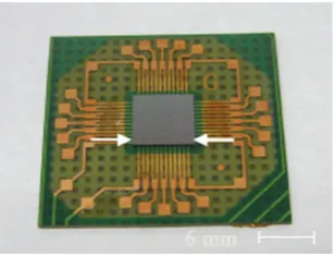
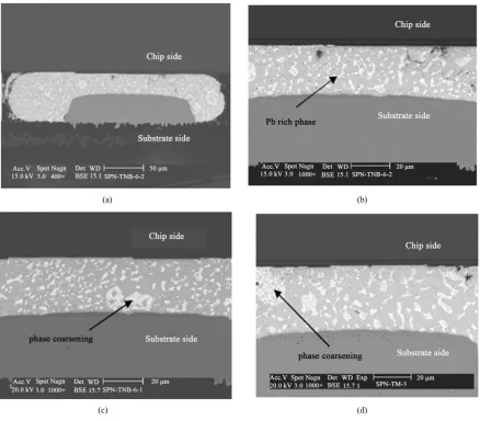
[image:8.595.237.391.384.501.2]D. Yang et al. (2006) [27] found in their experiment for eutectic SnPb flip chip solder joints, no significant thermomigration occurred after 100 h at 20˚C and at 100˚C. Only microstructural coarsening was observed in solder joints Figure 14. But at higher temperature 150˚C after 50 h they observed that Pb thermomigration and phase segregation. Figure 12 shows a typical bonded sample prepared for testing. A typical sketch of flip chip solder joints shown in Figure 13 has been used for this study where two pairs of solder joints (joint 5, 6, 7 and 8) were powered with a current of 1.8 A at different ambient temperatures.
[image:8.595.226.404.539.605.2]Figure 12. A Flip chip sample (The arrowed region shows the area which is given as an expanded sketch [27].
Figure 13.Sketch of solder joints with four solder joints (joint 5 to 8) under current stressing [27].
Table 1. Comparison of D × Z*.
Lee et al. (2001) Lee and Tu (2001) Hue Ye et al. (2003)
Temperature (˚C) Current density A/cm2
Time (h) D × Z*
120˚C 2 × 10⁴
324 2.16 × 10⁻¹¹
120˚C 3.8 × 10⁴
39.5 1.85 × 10⁻¹⁰
Room Temperature 1.3 × 10⁴
[image:8.595.96.540.658.723.2]experimentation [23]. D. Yang et al. (2006) [27] also explained coarsening in their literature. Figure 14(a) and Figure 14(b) are shown the original microstructure of solder joints before the experiments.
In the fine scale, bright region corresponds to the Pb rich region and dark region corresponds to the Sn rich region because of their difference in element numbers in the periodic table. When a current 1.8 A was applied of this solder joint at 20˚C and 100˚C after 100 h the phase coarsening were observed shown in Figure 14(c) and Figure 14(d) [11]. H. Ye et al. (2003) [23] also found in their experiment the average area and diameter of Pb rich regions were increasing according to current stressing time. The “average diameter” is calculated from the average length of several lines drawn through the centroid of the phase region and only the “average area” is an ASTM standard. The average Pb phase size and average Pb phase diameter of Pb regions vs. stressing time are shown in Figure 15.
(a) (b)
[image:9.595.95.534.303.687.2](c) (d)
(a) (b)
Figure15.Pb phase: (a) average area vs. stressing time; (b) average diameter vs. stressing time[23].
3. Mean Time to Failure (MTF) of Interconnection in IC
Due to difficulty of testing under real conditions of IC, at the end of the 1960s J. R. Black developed an empirical equation to estimate the MTF of a metal wire interconnection, taking EM into consideration and this equation has been widely used till now to predict the life time of ICs [15] [26] [28].
(
)
–(
)
crit
MTF=A J J− nexp E KTa
where, A = Constant based on the cross-sectional area of the interconnection;
J = Current density; Jcrit = Critical (threshold) current density necessary to produce failure;
Ea = Thermal activation energy (e.g. 0.7 eV for grain boundary diffusion in Al [29]);
K = Boltzmann’s Constant; T = Line temperature;
n = Scaling factor (usually set to 2 according to Black [30]).
So, it is clear from the above equation, current density (J) and the temperature (T) arethe affecting parameters at the MTF of the interconnection. During rising temperatures for an interconnection to remain reliable, the maxi-mum tolerable current density of the conductor must necessarily decrease. Usually, both the average J and average T are increasing as the semiconductor technology advances. Consequently, more precise EDA (Electronic design automation) tools that are able to account for the thermal effects are required to design in reliability which is nothing but to accurately simulate the current density and temperature of interconnects in order to prevent EM induce failures.
4. Importance of EM
EM is the dominate failure mechanism in Power ICs and decreases the reliability of chips integrated circuits (ICs). So Interconnect reliability is the main factor that determines the circuit reliability especially when the line width becomes much narrower which renders high current density [31]. It also noted that the failure rate of a scaled 65 nm processor is more than three times higher than a similarly pipelined 180 nm processor, where EM and time-dependent dielectric breakdown showing the most dominant mechanisms according to the advance-ment in the technology nodes.
Figure 16. Schematic of a simple inverter circuit to illustrate the in-creasing sensitivity of circuit performance to inter connect [19].
5. Improvement of Interconnect Reliability
From the EM studies it is noted that the interconnect reliability in ICs is most important issues as technology node advances in order to ensure its reliability. Recent work [32] showed that chip failures because of power grid issues, where EM already being discovered by chip designers. Analysis of power grid is becoming a re-quired addition to many design flows. The interconnect system is facing a number of different challenges ahead. Novel interconnect systems such as 3D interconnect are proposed and experimented, new interconnect materials are also being explored but the reliability of these new proposals remains unknown. C. Goossens et al. and J. Guo [23] [32] mentioned in their work additional efforts at the design stage are essential to obtain robust and re-liable chips. In order to provide adequate knowledge on the interconnect EM for both the IC manufacturers and designers, the testing methodologies of interconnect reliability and the modeling of EM is necessary. The mod-eling of EM is particularly important because it helps to identify the critical weak spots of an interconnection system in a short time. A typical IC layout has millions of interconnection. Analyzing the reliability problems on each of them is prohibitively time consuming. So using EM modeling the key interconnects easily can be inves-tigated. Also, modeling of EM can be integrated into EDA tool, where a complete EM aware IC design can be realized. Using the advancement in numerical tools, key factors that affect the EM performances of an intercon-nect system can be identified. Which is more significant for ULSI development so that a reliable interconintercon-nect system can be built as ULSI technology is advancing and the demand for ULSI in term of speed and functional-ity are ever increasing [14] [29]. Another recent work [15], where EM reliabilfunctional-ity of the contact hole in SiC pow-er devices was evaluated for an improved Al electrode sandwiched between thin TaN laypow-ers. They showed that Al electrode demonstrated long-term reliability even at higher junction temperatures. They found MTF of ap-proximately 3400 years under conditions of Tj = 300˚C and J = 104 A/cm2. On the other hand, many ICs have an
intended MTF is at least 10 years [17]. But in modern power electronic devices, power ICs are rarely fail due to EM effects, because most of the IC design houses use automated EDA tools to check and correct EM problems at the transistor layout-level. When devices are operated within the manufacturer’s specified temperature and voltage range, a properly designed IC device is more likely to fail from other causes may be environmental or such as cumulative damage from gamma-ray bombardment.
6. Conclusion
de-signers to more aggressively explore the design space and to reclaim the design margin imposed by less accurate, more pessimistic models. This analysis shows that temperature-aware designers are to evaluate the system relia-bility using runtime information, which increases the confidence about the actual behavior of the system. Gener-ally, when the operating temperature increases, lifetime is being consumed more rapidly and vice versa. But if the operating temperature is below a nominal temperature (i.e., the threshold temperature used in DTM tech-niques), lifetime can be easily consumed at a slower rather than nominal rate. This is nothing but banking time for future consumption. As a result, much better performance gains would be expected because more life-times can be banked.
References
[1] Weber, W.M. (2008) Silicon to Nickel Silicide Longitudinal Nanowire Heterostructures: Synthesis, Electrical Charac terization and Novel Devices. PhD Thesis, Technische University Munchen, Munich.
[2] Bourjot, E., Putero, M., Perrin-Pellegrino, C., Gergaud, P., Gregoire, M., Nemouchi, F. and Mangelinck, D. (2014) Kinetics Study of NiPt(10 at.%)/Si0.7Ge0.3 Solid State Reactions. Microelectronic Engineering, 120, 163-167.
http://dx.doi.org/10.1016/j.mee.2013.12.009
[3] Najm, F., Hajj, I. and Yang, P. (1989) Electromigration Median Time-to-Failure Based on a Stochastic Current Wave-form. IEEE International Conference on Computer Design, Cambridge, 2-4 October 1989, 447-450.
[4] Sigal, L., et al. (2011) Uniting to Overcome a Mounting BEOL Electromigration Reliability Challenge. Proceedings of IEEE International Conference on Computer-Aided Design, Munich, 7 November 2011.
[5] Pak, J., Pathak, M., Lim, S.K. and Pan1, D.Z. (2011) Modeling of Electromigration in Through-Silicon-Via Based 3D IC. IEEE 61st Electronic Components and Technology Conference, Lake Buena Vista, 31 May 2011-3 June 2011, 1420-1427.
[6] Jing, J.P., Liang, L. and Meng, G. (2010) Electromigration Simulation for Metal Lines. Journal of Electronic Packag-ing, 132, Article ID: 011002. http://dx.doi.org/10.1115/1.4000716
[7] Lienig, J. (2005) Interconnect and Current Density Stress: An Introduction to Electromigration-Aware Design. Pro-ceedings of IEEE SLIP, San Francisco, 2-3 April 2005, 81-88.
[8] Heliot, J.P. and Tullos, L. (2001) International SEMATE Technology Transfer. STMicroelectronics.
[9] Pak, J., Limet, S.K. and Pan, D.J. (2012) Electromigration-Aware Routing for 3D ICs with Stress-Aware EM Model-ing. Proceedings of IEEE International Conference on Computer-Aided Design, New York, 8 November 2012, 325- 332. http://dx.doi.org/10.1145/2429384.2429451
[10] Lee, J.H., et al. (2008) Size Effect on Electromigration Reliability of Pb-Free Flip Chip Solder Bump. IEEE 58th Elec-tronic Components and Technology Conference, Lake Buena Vista, 27-30 May 2008, 2030-2034.
[11] Tan, C.M. (2010) Electromigration in ULSI Interconnections. World Scientific Publishing Co. Pte. Ltd., Singapore.
http://www.worldscibooks.com/engineering/7294.html
[12] CSL (Computer Simulation Laboratory) (2011) Middle East Technical University.
http://www.csl.mete.metu.edu.tr/Electromigration/emig.htm
[13] DoITPoMS. TLP Library: Electromigation. University of Cambridge, Cambridge.
http://www.doitpoms.ac.uk/tlplib/electromigration/flux_2.php
[14] Nah, J.W., Kim, J.H., Lee, H.M. and Paik, K.-W. (2033) Electromigration in Flip Chip Solder Bump of 97Pb- 3Sn/37Pb-63Sn Combination Structure. Acta Materialia, 52, 129-136.
http://dx.doi.org/10.1016/j.actamat.2003.08.035
[15] Tanimoto, S., Nishio, N., Suzuki, T., Murakami, Y., Ohashi, H., Yamaguchi, H. and Okumura, H. (2010) Electromi-gration Reliability of the Contact Hole in SiC Power Devices Operated at Higher Junction Temperatures. Materials Science Forum, 645-648, 1139-1142.
[16] Islam, N., Kim, G. and Kim, K. (2014) Electromigration for Advanced Cu Interconnect and the Challenges with Re-duced Pitch Bumps. 2014 IEEE 64th Electronic Components and Technology Conference (ECTC), Orlando, 27-30 May 2014, 49-55. http://dx.doi.org/10.1109/ectc.2014.6897266
[17] Lienig, J. (2013) Electromigration and Its Impact on Physical Design in Future Technologies. Proceedings of the 2013 ACM International Symposium on International Symposium on Physical Design, Stateline, 24-27 March 2013, 33-40.
http://dx.doi.org/10.1145/2451916.2451925
[18] Zeng, K. and Tu, K.N. (2002) Six Cases Reliability Study of Pb-Free Solder Joints in Electronic Packaging Technolo-gy. Materials Science and Engineering, 38, 55-105. http://dx.doi.org/10.1016/S0927-796X(02)00007-4
Strain Evolution of Solder Joints. The 8th Intersociety Conference on Thermal and Thermomechanical Phenomena in Electronic Systems, San Diego, 1 June 2002, 946-952.
[23] Ye, H., Cemal, B. and Hopkins, D.C. (2003) Damage Mechanics of Microelectronics Solder Joints under High Current Densities. International Journal of Solids and Structures, 40, 4021-4032.
http://dx.doi.org/10.1016/S0020-7683(03)00175-6
[24] Blech, I.A. and Herring, C. (1976) Stress Generation by Electromigration. Applied Physics Letters, 29, 131-133.
http://dx.doi.org/10.1063/1.89024
[25] Lee, T.Y., Tu, K.N. and Frear, D.R. (2001) Electromigration of Eutectic SnPb and SnAg3.8Cu0.7 Flip Chip Solder
Bumps and Under-Bump Metallization. Journal of Applied Physics, 90, 4502-4508.
http://dx.doi.org/10.1063/1.1400096
[26] Nguyena, H.V., Salm, C., Krabbenbrgb, B., Zaage, K.W., Bisschopb, J., Mouthma, A.J. and Kuper, F.G. (2004) Effect of Thermal Gradients on the Electromigration Lifetime in Power Electronics. 42nd Annual International Reliability Physics Symposium, Phoenix, 25-29 April 2004, 619-620.
[27] Yang, D., Alam, M.O., Yu, B.Y. and Chan, Y.C. (2006) Thermomigration in Eutectic Tin-Lead Flip Chip Solder Joints. 8th Electronic Packaging Technology Conference, Singapore, 6-8 December 2006, 665-569.
http://dx.doi.org/10.1109/eptc.2006.342775
[28] Gui, X., James, W.H., Steven, K.D. and Michael, J.B. (1998) Simulation of Temperature Cycling Effects on Electro-migration Bhavior under Pulsed Current Stress. IEEE Transactions on Electron Devices, 45, 380-386.
http://dx.doi.org/10.1109/16.658670
[29] Young, D. and Christou, A. (1994) Failure Mechanism Models for Electromigration. IEEE Transactions on Reliability,
43, 186-192. http://dx.doi.org/10.1109/24.294986
[30] Black, J.R. (1969) Electromigration—A Brief Survey and Some Recent Results. IEEE Transactions on Electronic De-vices, 16, 338-347. http://dx.doi.org/10.1109/T-ED.1969.16754
[31] Tan, C.M. and Roy, A. (2007) Electromigration in ULSI Interconnects. Materials Sciences and Engineering, 58, 1-75.
http://dx.doi.org/10.1016/j.mser.2007.04.002
[32] Guo, J., Papanikolaou, A., Stucchi, M., Croes, K., TÖkei, Z. and Catthoor, F. (2008) The Analysis of System-Level Timing Failures Due to Interconnect Reliability Degradation. IEEE Transactions on Device and Materials Reliability,
![Figure 1. A cross-sectional view of the interconnect structure [12].](https://thumb-us.123doks.com/thumbv2/123dok_us/7978006.755902/2.595.158.472.446.707/figure-cross-sectional-view-interconnect-structure.webp)
![Figure 3. Voids form where the electrons flow away from the via, while a hillock forms when electrons flow towards the via [14]](https://thumb-us.123doks.com/thumbv2/123dok_us/7978006.755902/3.595.214.411.309.499/figure-voids-form-electrons-flow-hillock-forms-electrons.webp)
![Figure 5. Thermal acceleration loop during EM [19].](https://thumb-us.123doks.com/thumbv2/123dok_us/7978006.755902/4.595.188.500.80.198/figure-thermal-acceleration-loop-during-em.webp)
![Figure 6. (a) A schematic cross-section; (b) SEM secondary image of SnPb solder joint [23]](https://thumb-us.123doks.com/thumbv2/123dok_us/7978006.755902/5.595.135.493.341.675/figure-schematic-cross-section-secondary-image-snpb-solder.webp)
![Figure 8. SEM secondary images [23]. (a) after 37.5h, magnification 700×; (b) area on the PCB board side(anode) 2000×; (c) area on the silicon side(cathode) 2000×](https://thumb-us.123doks.com/thumbv2/123dok_us/7978006.755902/6.595.85.535.82.430/figure-secondary-images-magnification-board-anode-silicon-cathode.webp)
![Figure 9. Markers position on the cross-sectioned surface (initial SEM backscatter image) [23]](https://thumb-us.123doks.com/thumbv2/123dok_us/7978006.755902/7.595.209.420.510.702/figure-markers-position-cross-sectioned-surface-initial-backscatter.webp)
![Figure 16. Schematic of a simple inverter circuit to illustrate the in-creasing sensitivity of circuit performance to inter connect [19]](https://thumb-us.123doks.com/thumbv2/123dok_us/7978006.755902/11.595.196.428.81.262/figure-schematic-inverter-circuit-illustrate-creasing-sensitivity-performance.webp)
