N A N O E X P R E S S
Open Access
Control of epitaxial relationships of ZnO/SrTiO
3
heterointerfaces by etching the substrate surface
Caihong Jia
1,2, Yonghai Chen
1*, Xianglin Liu
1, Shaoyan Yang
1, Weifeng Zhang
2and Zhanguo Wang
1Abstract
Wurtzite ZnO thin films with different epitaxial relationships are obtained on as-received and etched (001), (011), and (111) SrTiO3(STO) by metal-organic chemical vapor deposition (MOCVD). ZnO films exhibit nonpolar (112―0) orientation with in-plane orientation relationship of <0001>ZnO//<110>STOon as-received (001) STO, and polar c-axis growth with <11―00>ZnO//<110>STOon etched (001) STO substrates. ZnO films change from polar (0001) to semipolar (101―2) oriented on as-received and etched (011) STO. On as-received and etched (111) STO, ZnO films show the same growing direction of polar (0001), but different in-plane orientations with 30° rotation. The change of epitaxial relationship of ZnO films on as-received and etched (001), (011), and (111) STO substrates is
accompanied with the increase of lattice mismatch, decrease of bond density, and increase of substrate surface roughness. In other words, the epitaxial relationships of ZnO/STO heterointerfaces can be controlled by etching the substrates. These results show that polar, nonpolar, and semipolar ZnO films for different applications can be grown epitaxially on STO substrates by MOCVD.
Keywords:ZnO, SrTiO3, Epitaxial
Background
Growth direction is a key element to determine the elec-trical and optical properties of ZnO thin films, and diffe-rent orientations are demanded for various applications [1,2]. Polar ZnO films with a c-axis perpendicular to the growth plane are required for the high electron mobility transistor structure, which depends on the realization of a high-density two-dimensional electron gas using electric polarization effects. The nonpolar and semipolar ZnO films with a horizontal and inclinedc-axis are expected to show higher emission efficiency in light-emitting diodes by eliminating or reducing the spontaneous and piezoelec-tric polarization fields [3-5].
SrTiO3 (STO) single crystal substrates have been widely used to deposit functional oxide films with super-conductivity, ferroelectricity, and ferromagnetism owing to lattice match. Compared with other common sub-strates for ZnO growth, the integration of wurtzite ZnO and perovskite STO combines the rich properties of pe-rovskites together with the superior optical and electrical
properties of wurtzites [6-9]. Thus, the ZnO/STO het-erojunction is expected to be applied in new multifunc-tional devices due to carrier limitation and coupling effect. On the other hand, it is found that the pretreat-ment method of (001) STO single crystal substrates will significantly influence the growth behaviors of thin films. For example, Pb(Zr,Ti)O3 [10] and (Sr,Ba)Nb2O6 [11] films show different growth modes and orientations on the TiO2- and SrO-terminated surfaces of (001) STO substrates, whereas SrRuO3 [12] and BaTiO3[13] films exhibit different initial morphology and crystallinity on the as-received and etched (001) STO substrates, re-spectively. However, there is little research about the growth behavior of ZnO films on as-received and etched (001), (011), and (111) STO substrates. Furthermore, the control of epitaxial relationships for ZnO on STO has not been investigated in detail.
In this paper, polar, nonpolar, and semipolar ZnO films are obtained on as-received and etched (001), (011), and (111) STO substrates by metal-organic chemical vapor deposition (MOCVD). X-ray θ-2θ and Ф scannings are performed to determine the out-of-plane and in-plane epitaxial relationships between ZnO films and STO substrates.
* Correspondence:[email protected]
1Key Laboratory of Semiconductor Material Science, Institute of
Semiconductors, Chinese Academy of Science, P.O. Box 912, Beijing 100083, People’s Republic of China
Full list of author information is available at the end of the article
Methods
The substrates used were (001), (011), and (111) STO single crystal wafers with sizes of 10 × 5 × 0.5 mm3. The as-received STO substrates were polished and cleaned by an organic solution, while the etched substrates were further conducted in buffered HF solutions at room temperature. ZnO films were grown on both as-received and etched STO substrates by a home-designed and made vertical low-pressure MOCVD reactor. Bubbled diethylzinc (DEZn) and pure oxygen were the reactants, and nitrogen gas was used as the carrier gas. The sam-ples were grown at 600°C for 30 min with the same bubbled diethylzinc flux and carrier gas flux of oxygen. The flow rate of the pure oxygen gas was set at 1 slpm, and the flow rate of DEZn was set at 16 sccm. The pres-sure of the chamber was kept at 76 Torr. The epitaxial relationships were determined by X-rayθ-2θ (X’Pert Pro MPD, PANalytical, Almelo, The Netherlands) and Ф scannings (TTR III, Rigaku, Tokyo, Japan) with CuKα radiation.
Results and discussion
Figure 1 shows the surface images of as-received and etched STO substrates taken by an atomic force micro-scope (AFM). It can be clearly seen that the STO surface varies from smooth for as-received to rough for etched. The surface roughness of as-received STO substrates is about 1 nm, while the etched STO surface is full of pits or trenches with a surface roughness of around 20 nm. Al-though some reports show that the surface of HF-etched STO is atomically flat with Ti-terminated surface since
Sr atom is much more sensitive to HF attack than Ti atom [14], the etched STO surface in the present case is full of pits or trenches. The STO used in this work may not be a perfect single crystal and is assumed to be made up of nanograins [15]. The HF solution permeates into the grain boundaries and dissolves Sr atoms on the lateral sides. As etching proceeds, the grains shrink and the grain boundaries widen in size, leading to the appearance of pits or trenches. The tilted angles of pits or trenches from the surface are estimated from AFM to be 56.4°, 41.8°, and 64.0° on etched (001), (011), and (111) STO substrates, respectively. The pits and/or trenches may serve as patterned substrates to control the growth direction of ZnO films, which is essentially important for practical applications.
X-ray θ-2θ and Ф scans were performed to identify the out-of-plane and in-plane orientation relationships between the films and substrates. In aФscan, the num-ber of peaks corresponds to the numnum-ber of planes for a particular family that possesses the same angleχ(0°<χ< 90°) with the crystal surface, while the separation tween peaks correlates with the angular separation be-tween the corresponding projections of the normals to the scanning family onto the crystal surface. The Ф angles of the ZnO films are respectively corrected by the Фscan of the STO substrates.
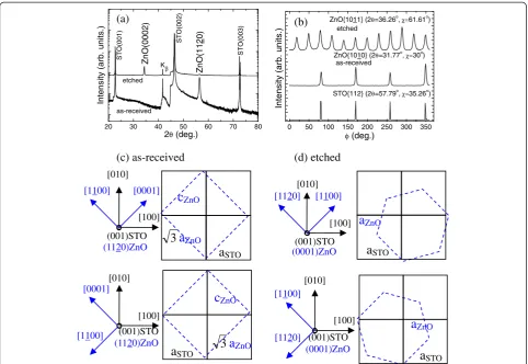
[image:2.595.58.539.480.716.2]It can be seen from Figure 2a that ZnO films show nonpolar (112―0) and polar (0001) orientations on as-received and etched (001) STO substrates, respectively. We first discuss the epitaxial relationship of (112―0) ZnO on as-received (001) STO. Several groups have obtained
(112―0) ZnO epitaxial films on (001) STO, but suppose one-, two-, or four-domain epitaxy [7-9,16]. In order to clarify the epitaxial relationship of (112―0)ZnO/(001) STO in the present work, we performed theФscans of ZnO {101―0} and STO {112} families, as shown in Figure 2b. In single crystal (112―0) ZnO, only two crystal planes in the ZnO {101―0} family have the same angle with the surface (χ = 30°), and two peaks separated by 180° are expected in ZnO {101―0}Фpatterns, which is just the case in single-domain (112―0) ZnO on r-sapphire [17]. However, the reflections from the ZnO {101―0} family show four peaks separated by 90°, implying that two domains perpendicular to each other coexist in the film plane. Furthermore, the peak positions in the Фscans of ZnO {101―0} (2θ = 31.77°,χ= 30°) and STO {112} (2θ= 57.79°,χ= 35.26°) coincide, implying that their zone axes are parallel to each other, that is, <0001>ZnO∥<110>STO, as shown in Figure 2c. In addition, the lattice mismatches are −5.7% (cZnO ffiffi2
p aSTO
ffiffi 2 p
aSTO ),
1.9% ( ffiffi3 p
aZnO ffiffi2
p aSTO
ffiffi 2 p
aSTO ) and −1.8% (
ffiffiffiffiffiffiffiffiffiffiffiffiffiffiffiffiffiffiffiffiffiffiffiffiffiffiffi 3
p aZnO
ð Þ2
þc2 ZnO
q
2aSTO
2aSTO )
along the directions of <0001>ZnO, <11―00>ZnO, and <11―01>ZnOin the film plane, respectively.
Similarly, the in-plane orientation relationships for (0001) ZnO films on etched (001) STO can also be achieved from X-ray Ф scanning. Figure 2b displays 12 peaks separated by 30° for the ZnO {101―1} family, which has six planes intersecting the surface at 61.6°. It indi-cates that two domains with 30° rotation coexist. Com-paring the peak positions of the ZnO {101―1} (2θ = 36.26°, χ = 61.61°) and STO {112} (2θ = 57.79°, χ = 35.26°), the in-plane orientation relationship is demon-strated to be <112―0>ZnO//<110>STOfor (0001) ZnO on etched (001) STO substrates, and the atomic arrange-ments are shown in Figure 2d. The lattice mismatch in the direction of <11―00>ZnO is 1.9% ( pffiffi3aZnO ffiffi2
p
aSTO
ffiffi
2 p
aSTO ), whereas in the direction of <112―0>ZnO, a higher order matching with a mismatch of −1.9% can also be found for seven ZnO over six STO unit cells. The higher order matching has been proposed for the epitaxial growth in large lattice mismatch system [18], but the lower order matching is regarded as the leading growth mechanism. Although the lattice mismatch of the (112―0) and (0001) ZnO with (001) STO are almost the same along <11―00>ZnO, (0001)-oriented films are obtained on etched (001) STO. This result is considered to be
0 50 100 150 200 250 300 350
ZnO{1011} (2θ=36.26o , χ=61.61o
)
ZnO{1010} (2θ=31.77o, χ=30o)
STO{112} (2θ=57.79o , χ=35.26o
)
Intensity (arb. units.)
φ (deg.)
as-received etched (b) (a) [100] (001)STO [010] [1100] [0001] (1120)ZnO
a
STOc
ZnO3
a
ZnOc
ZnO3
a
ZnOa
STO [100] [010] (001)STO [0001] [1100] (1120)ZnO (c) as-receiveda
ZnOa
STO [100] [010] (001)STO [1100] [1120] (0001)ZnO (d) etcheda
STOa
ZnO [100] [010] (001)STO [1120] [1100] (0001)ZnO20 30 40 50 60 70 80
etched STO(003) STO(002) ZnO(112 0) ZnO(0002)
Intensity (arb. units.)
2θ (deg.)
STO(001)
[image:3.595.57.540.88.420.2]as-received Kβ
related to the fact that ZnO films tend to be oriented in the (0001) direction even on amorphous substrates [19], implying that the restriction of substrates decreases and the surface energy becomes dominant for the growth of ZnO films on etched (001) STO. As a result, the (0001)
plane having the lowest surface energy, the close-packing plane tends to be oriented on etched (001) STO substrates.
Figure 3a shows that ZnO films exhibit (0002) and (101―2) preferred orientations on as-received and etched (011) STO substrates. The angle between (101―2) and
0 50 100 150 200 250 300 350
φ (deg.)
ZnO{0002} (2θ=34.42o, χ=42.77o)
ZnO{1011} (2θ=36.26ο, χ=61.61o
)
STO{100} (2θ=22.76ο, χ=45o)
Intensity (arb. units.)
as-received
etched
20 30 40 50 60 70 80
ST
O
(022)
ZnO(101
2)
2θ (deg.)
ZnO(0004)
ZnO(0002) K
K
STO
(011)
Intensity (arb. units.)
as-received etched
(a) (b)
(c) as-received
a
ZnO2
a
STOa
STO [1120][100] [011]
(011)STO
[1100]
(0001)ZnO
(d) etched
a
ZnO2
a
STOa
STO [3032][100] [011]
(011)STO
[1210]
(1012)ZnO
2 2
ZnO ZnO
c
[image:4.595.57.540.87.343.2]a
+
Figure 3ZnO films on as-received and etched (011) STO substrates.X-rayθ-2θ(a) andФ(b) scanning patterns and atomic arrangements (c,d).
20 30 40 50 60 70 80
2θ (deg.)
ZnO(0004)
ZnO(0002)
K K
ST
O
(111)
Intensity (arb. units.) as-received etched
(a)
(b)
2 a
STOa
ZnO [1100][011] [211]
(111)STO
[1120]
(0001)ZnO
(c) as-received
2 a
STOa
ZnO [1120]][011] [211]
(111)STO
[1100]
(0001)ZnO
(d) etched
0 60 120 180 240 300 360 ZnO{1122} (2θ=67.95o, χ=58.03o)
φ (deg.)
Counts (arb. units.)
STO{110} (2θ=32.40o, χ=35.26o) ZnO{1122} (2θ=67.95o, χ=58.03o)
etched
[image:4.595.57.540.459.714.2]as-received
bonded O atom
(b) as-received
[0001]
[110] [110]
(001)STO
[1100]
(1120)ZnO
[1100]
[110] [110]
(001)STO
[1120]
(0001)ZnO
O atom with dangling bond bonded O atom
(d) etched
Ti atom on STO surface O atom in ZnO layer
(a) as-received
[image:5.595.59.538.90.423.2]Ti atom on STO surface O atom in ZnO layer
(c) etched
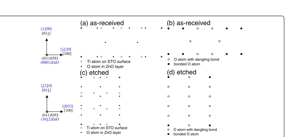
Figure 5The ZnO/(001)STO interface.Schematic top views (a,c) and distribution of O atoms bonded to Ti atoms (b,d) of the ZnO/(001)STO interface, in which (a,b) are on as-received STO while (c,d) are on etched STO. Only the O atoms and Ti atoms closest to the interface are shown in (a,c).
[1120]
[100] [011]
(011)STO
[1100]
(0001)ZnO
[3032]
[100] [011]
(011)STO
[1210]
(1012)ZnO
O atom with dangling bond bonded O atom
(b) as-received
Ti atom on STO surface O atom in ZnO layer
(c) etched
Ti atom on STO surface O atom in ZnO layer
(a) as-received
O atom with dangling bond bonded O atom
(d) etched
[image:5.595.59.540.464.696.2](0002) is calculated to be 42.77°, which corresponds to the tilted angle of the trench in etched (011) STO (41.8°, as shown in Figure 1d). This phenomenon is similar to that of GaN on patterned (001) Si substrates [20]. The ZnO films on as-received (011) STO show similar X-ray θ-2θ and Ф scanning patterns with other reports [6,7], and the atomic arrangements are shown in Figure 3c. The in-plane orientation relationship obtained was <11―00>ZnO∥<011>STO by comparing the Ф scanning peak positions of ZnO {101―1} (2θ = 36.26°, χ = 61.61°) and STO {100} (2θ = 22.76°, χ = 45°). The lattice mis-matches are 1.9% ( ffiffi3
p aZnO ffiffi2
p aSTO
ffiffi 2 p
aSTO ) and −16.8% (
aZnOaSTO
aSTO )
along the directions of <11―00>ZnO and <112―0>ZnO in the film plane, respectively. For (101―2) ZnO films on etched (011) STO, the in-plane orientation relation-ship obtained was<1―21―0>ZnO∥<011>STO by comparing the Ф scanning peak positions of ZnO {0002} (2θ= 34.42°, χ = 42.77°) and STO {100} (2θ = 22.76°,
χ = 45°). The lattice mismatches are −41.2%
(aZnOffiffi 2aSTO
2 p
aSTO ) and 57.1% (
aZnOþcZnOaSTO
aSTO ) along the
[image:6.595.61.539.344.704.2]directions of <112―0>ZnO and <3―032>ZnO in the film plane, respectively. Compared with ZnO films on the as-received (011) STO, much larger lattice mis-matches are found for those on etched (011) STO substrates.
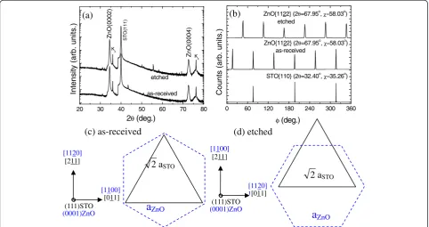
Figure 4a shows that ZnO films exhibit ac-axis perpen-dicular to the growth plane on both as-received and etched (111) STO substrates. Only six peaks are observed for the ZnO {112―2} family, which has six crystal planes with the same angle as the growth plane (χ= 58.03°), as shown in Figure 4b. Thus, both ZnO films are single-domain epitaxy on as-received and etched (111) STO, which exhibit a 30° rotation of the in-plane orientation. From the relative po-sition of ZnO {112―2} (2θ = 67.95°, χ = 58.03°) and STO {110} (2θ = 32.40°, χ = 35.26°) families, the in-plane relationships obtained was <11―00>ZnO∥<01―1>STO and <112―0>ZnO∥<01―1>STO on as-received and etched (111) STO substrates, respectively. The atomic arrangements in
[1100]
[011] [211]
(111)STO
[1120]
(0001)ZnO
[1120] ][011] [211]
(111)STO
[1100]
(0001)ZnO
(b) as-received
O atom with dangling bond bonded O atom
Ti atom on STO surface O atom in ZnO layer
(c) etched
Ti atom on STO surface O atom in ZnO layer
(a) as-received
O atom with dangling bond bonded O atom
(d) etched
the heterointerface of (0002)ZnO/(111)STO are shown in Figure 4c,d. The lattice mismatch is 1.91% ( ffiffi3
p aZnO ffiffi2
p aSTO
ffiffi 2 p
aSTO )
along the direction of <11―00>ZnO on as-received (111) STO, while the lattice mismatch is about 17.7% (2aZnO ffiffi2
p aSTO
ffiffi 2 p
aSTO ) along the direction of <112
―
0>ZnOon etched (111) STO. Surprisingly, the lattice mismatch increases a lot, but high quality with single-domain epitaxy is still pre-served on etched (111) STO substrates. A similar phenomenon is also found in (0001) ZnO films on (111) BaTiO3 pesudo-substrates [21]. The interface of ZnO on etched (111) STO is supposed to be incoherent, and the interface chemical energy plays a more important role than interface elastic energy for a large lattice mismatch system; thus, the excessive interface stress induces the rotation of ZnO domains.
Interestingly, all ZnO films prefer to grow with a much larger lattice mismatch on etched (001), (011), and (111) STO substrates. It is supposed that the inter-face dominates the film growth on as-received and etched STO, so it is essential to estimate the interface bond densities for each ZnO/STO heterointerface. To estimate the interface bond densities for each in-plane epitaxial relationship [22], we consider the in-plane atomic arrangements at the ZnO/STO interface for the case of as-received and etched STO surfaces. Figures 5a,c, 6a,c, and 7a,c show schematic top views of the ZnO/STO interfaces on as-received and etched (001), (011), and (111) STO substrates, respectively. In these figures, only the O atoms and Ti atoms closest to the interface are shown. Due to the large in-plane lattice mismatch between ZnO and STO, the arrangements of Ti-O bonds show the superstructure. In Figures 5b,d, 6b,d, and 7b,d, Ti-O bonds and dangling bonds are indi-cated by closed and open circles, respectively. Accord-ingly, the bond densities obtained were 3.41 × 10¹⁴and 1.09 × 1014 cm−2on as-received and etched (001) STO substrates, 3.28 × 10¹⁴ and 0.50 × 1014 cm−2 on as-received and etched (011) STO substrates, and 3.65 × 10¹⁴ and 1.31 × 1014 cm−2 on as-received and etched (111) STO substrates, respectively. Obviously, compar-ing with those on as-received STO, the bond density decreases greatly for ZnO films on etched STO. It is consistent with the fact that the substrate surface changes from smooth for as-received STO to rough for etched STO, as shown in Figure 1. With increasing sub-strate surface roughness, it becomes difficult to bond ZnO films and etched STO substrates, and the bond density decreases while the lattice mismatch increases largely for ZnO on etched STO. Therefore, the epitaxial relationship of ZnO/STO heterointerfaces can be controlled by etching the substrates.
Conclusions
In summary, epitaxial ZnO thin films have been obtained on as-received and etched (001), (011), and (111) STO substrates by MOCVD, and the epitaxial rela-tionships were determined. It is interesting that ZnO films exhibit nonpolar (112―0) orientation with an in-plane orientation relationship of <0001>ZnO//<110>STO on as-received (001) STO, and polar (0001) orientation with <11―00>ZnO//<110>STO on etched (001) STO sub-strates, respectively. The surface energy is supposed to be dominant for c-axis growth on etched (001) STO. ZnO films change from polar (0001) orientation to semi-polar (101―2) orientation on as-received and etched (011) STO. On as-received and etched (111) STO, ZnO films show the same growth direction with polar (0001), but different in-plane orientation with 30° rotation and a large lattice mismatch induced by the extra interface chemical energy of etched (111) STO with more dan-gling bonds. The change of epitaxial relationship for ZnO films on as-received and etched STO substrates is accompanied with the increase of lattice mismatch, de-crease of bond density, and inde-crease of substrate surface roughness. This investigation presents a very simple way to control epitaxial relationship of ZnO films with STO substrates, which is of technological interest in optoelec-tronic and elecoptoelec-tronic devices.
Competing interests
The authors declare that they have no competing interests.
Authors’contributions
CJ carried out the experimental analysis and drafted the manuscript. YC carried out the experimental design. XL carried out the growth and optimization of indium nitride films. SY participated in the experimental measurement. WZ participated in its design and coordination. ZW participated in the experimental design. All authors read and approved the final manuscript.
Acknowledgments
This work was supported by the 973 program (2012CB921304, 2012CB619306) and the National Natural Science Foundation of China (60990313, 51202057).
Author details
1Key Laboratory of Semiconductor Material Science, Institute of
Semiconductors, Chinese Academy of Science, P.O. Box 912, Beijing 100083, People’s Republic of China.2Key Laboratory of Photovoltaic Materials of
Henan Province and School of Physics and Electronics, Henan University, Kaifeng 475004, People’s Republic of China.
Received: 5 December 2012 Accepted: 2 January 2013 Published: 10 January 2013
References
1. Perez JZ, Sanjose VM, Lidon EP, Cochero J:Facets evolution and surface electrical properties of nonpolarm-plane ZnO thin films.Appl Phys Lett
2006,88:261912.
3. Perez JZ, Sanjose VM, Lidon EP, Colchero J:Polarity effects on ZnO films grown along the nonpolar [11–20]-direction.Phys Rev Lett2005,
95:226105.
4. Baker TJ, Haskell BA, Wu F, Fini PT, Speck JS, Nakamura SJ:Characterization of planar semipolar gallium nitride films on spinel substrates.Jpn J Appl Phys2005,44:L920.
5. Peruzzi M, Pedarnig JD, Bauerle D, Schwinger W, Schaffler F:Inclined ZnO thin films produced by pulsed-laser deposition.Appl Phys A1873,
2004:79.
6. Bellingeri E, Marre D, Pallecchi I, Pellegrino L, Siri AS:High mobility in ZnO thin films deposited on perovskite substrates with a low temperature nucleation layer.Appl Phys Lett2005,86:012109.
7. Wei XH, Li YR, Zhu J, Huang W, Zhang Y, Luo WB, Ji H:Epitaxial properties of ZnO thin films on SrTiO3 substrates grown by laser molecular beam epitaxy.Appl Phys Lett2007,90:151918.
8. Wu YL, Zhang LW, Xie GL, Zhu JL, Chen YH:Fabrication and transport properties of ZnO/Nb-1 wt%-doped SrTiO3epitaxial heterojunctions. Appl Phys Lett2008,92:012115.
9. Karger M, Schilling M:Epitaxial properties of Al-doped ZnO thin films grown by pulsed laser deposition on SrTiO3(001).Phys Rev B2005, 71:075304.
10. Fujisawa H, Nonomura H, Shimizu M, Niu H:Observations of initial growth stage of epitaxial Pb(Zr, Ti)O3 thin films on SrTiO3(1 0 0) substrate by MOCVD.J Crystal Growth2002,237–239:459.
11. Infortuna A, Muralt P, Cantoni M, Setter N:Epitaxial growth of (Sr, Ba) Nb2O6 thin films on SrTiO3 single crystal substrate.J Appl Phys2006,
100:104110.
12. Chae RH, Rao RA, Gan Q, Eom CB:Initial stage nucleation and growth of epitaxial SrRuO3thin films on (0 0 1) SrTiO3substrates.J Electroceramics
2000,4:345.
13. Yoshimura T, Fujimura N, Ito T:The initial stage of BaTiO3epitaxial films on etched and annealed SrTiO3substrates.J Crystal Growth1997,174:790.
14. Kawasaki M, Takahashi K, Maeda T, Tsuchiya R, Shinohara M, Ishiyama O, Yonezawa T, Yoshimoto M, Koinuma H:Atomic control of the SrTiO3 crystal surface.Science1994,266:1540.
15. Li ZH, Sun HT, Xie ZQ, Zhao YY, Lu M:Modulation of the
photoluminescence of SrTiO3(001)by means of fluorhydric acid etching combined with Ar+ion bombardment.Nanotechnology2007,18:165703. 16. Wu YL, Zhang LW, Xie GL, Ni J, Chen YH:Structural and electrical
properties of (110) ZnO epitaxial thin films on (001) SrTiO3substrates. Solid State Communinations2008,148:247.
17. Han SK, Hong SK, Lee JW, Lee JY, Song JH, Nam YS, Chang SK, Minegishi T, Yao T:Structural and optical properties of non-polar A-plane ZnO films grown on R-plane sapphire substrates by plasma-assisted molecular-beam epitaxy.J Crystal Growth2007,309:121.
18. Zheleva T, Jagannadham K, Narayan J:Epitaxial-growth in large-lattice-mismatch systems.J Appl Phys1994,75:860.
19. Funakubo H, Mizutani N, Yonetsu M, Saiki A, Shinozaki KJ:Orientation control of ZnO thin film prepared by CVD.Electroceramics1999,4:25. 20. Hikosaka T, Honda Y, Yamaguchi M, Sawaki N:Al doping in (1–101) GaN
films grown on patterned (001) Si substrate.J Appl Phys2007,101:103513. 21. Wei XH, Li YR, Jie WJ, Tang JL, Zeng HZ, Huang W, Zhang Y, Zhu J:
Heteroepitaxial growth of ZnO on perovskite surfaces.J Phys D: Appl Phys
2007,40:7502.
22. Hirama K, Taniyasu Y, Kasu M:Heterostructure growth of a single-crystal hexagonal AlN (0001) layer on cubic diamond (111) surface.J Appl Phys
2010,108:013528.
doi:10.1186/1556-276X-8-23
Cite this article as:Jiaet al.:Control of epitaxial relationships of ZnO/ SrTiO3heterointerfaces by etching the substrate surface.Nanoscale
Research Letters20138:23.
Submit your manuscript to a
journal and benefi t from:
7Convenient online submission
7Rigorous peer review
7Immediate publication on acceptance
7Open access: articles freely available online
7High visibility within the fi eld
7Retaining the copyright to your article