International Journal of Emerging Technology and Advanced Engineering
Website: www.ijetae.com (ISSN 2250-2459,ISO 9001:2008 Certified Journal, Volume 4, Issue 3, March 2014)
365
Performance Analysis and Implementation of CMOS Current
Starved Voltage Controlled Oscillator for Phase Locked Loop
NehaPathak
1, Prof. Ravi Mohan
21
M Tech Scholar, Dept of ETC, SRIT Jabalpur (M.P),India, 2HOD M tech Dept of ETC, SRIT Jabalpur (M.P), India
Abstract— The work is based on Current Starved Voltage controlled oscillator (CSVCO) for a Phase Locked Loop (PLL) in 180 nm process. Phase locked loop’s were used in most of the application for clock generation and recovery as well. As the technology grows faster in the existing generation, there has to be quick development with the technique.
In most of the application PLL’s were used for clock and data recovery purpose, from that perspective jitter will stand as a huge problem for the designers. The main aim of this thesis was to design a Current Starved Voltage controlled oscillator (CSVCO) that should bring down the jitter as down as possible which was designed as standalone; the designed CSVCO would be later placed in a PLL. To understand the concept and problem about jitter at the early stage of the project, an Analog PLL was designed in block level and tested for different types of jitter and then design of a CSVCO was started. This document was about the design of a Current Starved Voltage controlled oscillator which operates with the center frequency of 1.25 GHz.
This project work describes the design and simulation of miscellaneous blocks of an PLL for the 3.33 GHz band. The reference frequency is 500 MHz and the Current Starved Voltage controlled oscillator output frequency is 1.25 GHz to 3.33 GHz in a state-of the-art 180nm process, with 1 V supply voltage.
Keywords- CSVCO; PLL; Zeni˗EDA; Oscillation
frequency; power consumption.
I. INTRODUCTION
A PLL is a feedback system that compares the output frequency/phase with the input frequency/phase. Phase-locked loops can be utilized for frequency synthesizing, carrier synchronization, carrier recovery, frequency
division, frequency multiplication and frequency
demodulation [1]. A PLL is generally used in wireless communications and data recovery circuits. A VCO is the heart of the PLL and can be designed either by LC or RC. A LC VCOs have superior phase noise performance compared with ring VCO’S. However, an LC VCO has a small tuning range large layout area and possibly higher power [2]. The ring oscillators, however, do not have the complication of the on-chip inductors required for the LC oscillators. Thus the chip area is reduced. In addition to a wide tuning range; ring oscillators with even number of delay cells can produce quadrature-phase outputs.
The phase noise performance of ring oscillators is much poorer in general [3], [4]. Also, at high oscillation frequencies, the power consumption of the ring oscillators may not be low which is a key requirement for battery operated devices [5]. To overcome these problems, we work on five stages current starved Oscillator and single stage source coupled oscillator without an LC tank. Finally their performances are compared based on their results.
A challenging work in the CMOS technology is to design a low phase noise ring oscillator for a Charge Pump Phase Locked Loop (CPPLL) using CMOS technology. A design presented here is to improve the overall characteristics of PLL. The first component of the PLL is the PFD which has been designed to improve the speed by minimizing the dead zone. The CP circuit improves the performance of the PLL because it has been designed for high bandwidth. The main part of this PLL is the CSVCO, which has been designed to get superior phase noise.
II.SYSTEM OVERVIEW
Phase-locked loops (PLLs) generate well-timed on-chip clocks for various applications such as clock and data recovery, microprocessor clock generation and frequency synthesizer. The basic concept of phase locking has remained the same since its invention in the 1930s [1]. However, design and implementation of PLLs continue to be challenging as design requirements of a PLL such as clock timing uncertainty, power consumption and area become more stringent.
This section briefly discusses the basic concept of phase locking. A PLL is a closed-loop feedback system that sets fixed phase relationship between its output clock phase and the phase of a reference clock. A PLL tracks the phase changes that are within the bandwidth of the PLL.
International Journal of Emerging Technology and Advanced Engineering
Website: www.ijetae.com (ISSN 2250-2459,ISO 9001:2008 Certified Journal, Volume 4, Issue 3, March 2014)
366
After this, the PLL continues to compare the two signals but since they are in lock mode, the PLL output is constant.
A basic form of a PLL consists of five main blocks:
1. Phase Frequency Detector (PFD) 2. Charge Pump (CP)
3. Low Pass Filter (LPF)
4. Voltage Controlled Oscillator (VCO) 5. Frequency divider
III. PLLARCHITECTURE
To synchronize the frequency, various types of PLLs are being used in the application of wireless communication. PLLs are consists of PFD, CP, LPF, CSVCO and divider which is shown in Fig. 1. In addition with CSVCO, the PFD compares feedback signal with input signal and generates the error signal. A charge pump circuit along with LPF is used to minimize the disturbances at the input of CSVCO and to get a sharper and smooth signal at the CSVCO output. To form a phase-locked loop (PLL), the phase error output of PFD is fed to a charge pump and then to loop filter which integrates the signal to get a sharper and smooth signal so that the disturbances at the input of CSVCO get minimized.
Figure (1): Architecture of PLL
IV. CURRENT-STARVED VOLTAGE CONTROLLED
OSCILLATOR
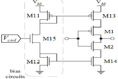
The operation of current starved VCO is similar to the ring oscillator. Figure (2) shows a one stage Current˗ Starved VCO [6]. Middle PMOSM1 and NMOSM2 operate as inverter, while upper PMOSM11 and lower NMOSM14 operate as current sources. The current sources limit the current available to the inverter. In other words, the inverter is starved for current. The current in the first NMOS and PMOS are mirrored in each inverter/current source stage. PMOSM11 and NMOSM11 drain currents are the same and are set by the input control voltage [6].
Figure (2): current starved with output-switching
The current-starved VCO is as shown in Figure (2) with the current-starved structure, the supply noise would contaminate the output phase. Referring to (6), the output frequency can be assumed to be in terms of the RC delay
and n denoting the number of the inverter stages. Ctot
denotes the total parasitic capacitance including wire
parasitic capacitor (Cwire), and drain-to-bulk capacitor
(CDB). For simplifying the analysis, CDB is assumed to be a
constant regardless of the operation mode of the transistors. Moreover, the resistance of the channel of each stage (R)
could be estimated as the reciprocal of the
transconductance of the MOS. With
the
supply noise would change the VGS of the PMOS and
further affect the output frequency and output phase:
=
( )( )
Where VTH denotes the threshold voltage [11].
[image:2.612.346.550.141.278.2] [image:2.612.53.284.413.519.2]International Journal of Emerging Technology and Advanced Engineering
Website: www.ijetae.com (ISSN 2250-2459,ISO 9001:2008 Certified Journal, Volume 4, Issue 3, March 2014)
367
The currents in M5 and M6 are mirrored in each inverter/current source stage. There are in total 23 transistors, where upper PMOS transistors are connected to the gate of M6 and source voltage is applied to the gates of all lower NMOS transistors [9].
Figure (3) Schematic Circuit of Current-Starved VCO
Now the performance analysis for the CSVCO is as shown in Table (1) with different voltages for generating the different frequencies.
Table (1)
CSVCO output frequency range
S. No.
CSVCO input control Voltage in (Volts)
Output frequency in (GHz)
1 0.4 0.04
2 0.6 0.53
3 0.8 1.25
4 1.0 1.66
5 1.1 2.0
6 1.2 2.5
7 1.3 2.5
8 1.4 2.8
9 1.5 3.1
10 1. 7 3.3
V.PHASE FREQUENCY DETECTOR
A phase frequency detector (PFD), is a device which compares the phase of two input signals and provides a signal in the form of phase error.
It has two inputs which correspond to two different input signals, usually one from a current starved voltage-controlled oscillator and other is a reference source. It has two outputs which instruct subsequent circuitry on how to adjust to lock onto the phase [10].
From Figure (4) the Schematic Circuit of Phase Frequency Detector compares the leading edges of data and data1 (data is the input signal to PFD, data1 is considered as the feedback signal from the output of VCO to PFD). A data1 rising edge cannot be present without a data rising edge. If the rising edge of the data leads the data1 rising edge, the "Up" output of the phase detector goes high while the "Down" output remains low. This causes the data1 frequency to increase and makes the edges move closer. If the data1 signal leads the data, "Up" remains low while the "Down" goes high. And we can find the phase difference between data1 and data.
Figure (4) Schematic Circuit of Phase Frequency Detector
VI. CHARGE PUMP
[image:3.612.48.302.194.413.2] [image:3.612.351.535.336.469.2] [image:3.612.57.281.489.619.2]International Journal of Emerging Technology and Advanced Engineering
Website: www.ijetae.com (ISSN 2250-2459,ISO 9001:2008 Certified Journal, Volume 4, Issue 3, March 2014)
368
Figure (5) Schematic Circuit of Charge Pump
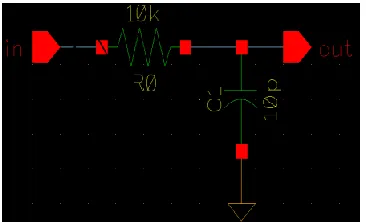
VII. LOOP FILTER
The function of the loop filter is to convert the output signal of phase frequency detector to control voltage and also to filter out any high frequency noise introduced by the PFD. The loop filter shown in Figure (6) used with this type of PFD is a simple RC low-pass filter. Since the output of the PFD is oscillating, the output of the loop filter will show a ripple as well, even when the loop is locked. This modulates the clock frequency, an unwanted characteristic of a DPLL using PFD. A ripple on the output of the loop filter with a frequency equal to the clock frequency will modulate the control voltage of the VCO. A high speed low power consumption positive edge triggered Delayed (D) flip-flop was designed for increasing the speed of counter in Phase locked loop, using 180 nm CMOS technology.
Figure (6): Low Pass Filter
VIII.FREQUENCY DIVIDER
Frequency divider divides the VCO frequency to generate a frequency which is comparable with reference
frequency. Here we used divide by 2 network, we can vary
the divider network for synthesis of different frequencies. It divide the clock signal of VCO and generate dclock as shown in figure (7), than applied to phase frequency detector which compare it with input data[8].
Figure (7) Schematic Circuit of Frequency divider
IX. RESULTS AND WAVEFORMS
The PLL for high performance application have been designed using 180 nm CMOS technology with 36.516 mA. and emulated by Zeni Electronic Design Automation . The phase noise obtained is-122.2 dBc/Hz @ 10 MHz offset frequency, which is shown in Fig. (8). The proposed voltage controlled oscillator has designed for getting optimized 2.2 GHz frequency. A design has been completed with 180 nm CMOS technology and 1.5 Volt supply voltage. The final output waveform of complete PLL is shown in Figure (9). Where signal1 is for input data signal, signal2 is for output of PFD UP signal, signal3 is for output of PFD DN signal, signal4 is output charge pump, signal5 is output of Low Pass Filter, signal6 is output of current starved voltage controlled oscillator, and signal7 is output of divider circuit which is performing divide by 2 operation.
[image:4.612.79.260.132.257.2] [image:4.612.341.552.137.284.2] [image:4.612.78.261.472.583.2] [image:4.612.328.561.519.661.2]International Journal of Emerging Technology and Advanced Engineering
Website: www.ijetae.com (ISSN 2250-2459,ISO 9001:2008 Certified Journal, Volume 4, Issue 3, March 2014)
369
Figure (9): Waveforms of different stages of output signal for PLL
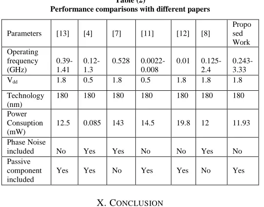
Now the results of PLL using CSVCO is compared with different papers in the parameters of operating frequency, power consumption etc. in Table (2).
Table (2)
Performance comparisons with different papers
Parameters [13] [4] [7] [11] [12] [8]
Propo sed Work Operating
frequency (GHz)
0.39-1.41
0.12-1.3
0.528 0.0022-0.008
0.01 0.125-2.4
0.243-3.33 Vdd 1.8 0.5 1.8 0.5 1.8 1.8 1.8
Technology (nm)
180 180 180 180 180 180 180
Power Consuption (mW)
12.5 0.085 143 14.5 19.8 12 11.93
Phase Noise
included No Yes Yes No No Yes No Passive
component included
Yes Yes No Yes Yes No Yes
X.CONCLUSION
Modern wireless communication system employ phase locked loop (PLL) mainly on synchronization clock synthesis, skew and jitter reduction. Because in the increase of speed of the circuit operation, there is a need of a PLL circuit with faster locking ability. The PLL has been designed with low power, small chip size area and better phase noise using 180 nm CMOS technology for high performance PLL and simulated by ZENI˗ EDA environment. While increasing the number of stages for getting the higher frequency the power dissipation and size of oscillator was going to increase. Hence instead of increasing the number of stages and time constant again a control voltage and width of the CMOS can be adjusted for getting the higher frequency.
REFERENCES
[1 ] J. Craninckx and M. Steyaert, “A 1.8-GHz low-phase noise CMOS VCO using optimized hollow spiral inductors,” IEEE J. Solid-State Circuits, vol. 32, pp. 736–744, May 1997.
[2 ] Yalcin, A.E. and P. John, 2004. A 5.9-GHz voltage controlled ring oscillator in 0.18 um CMOS technology. IEEE J. Solid-State Circuit, 39(1): 230-233.
[3 ] C. H. Park and B. Kim, “A low-noise, 900-MHz VCO in 0.6-_m CMOS,” IEEE J. Solid-State Circuits, vol. 34, pp. 586–591, May 1999.
[4 ] A. Hajimiri, S. Limotyrakis, and T. H. Lee, “Phase noise in multi- gigahertz CMOS ring oscillators,” in Proc. IEEE 1998 Custom Integrated Circuit Conf., 1998, pp. 49–52.
[5 ] T. Friedrich, “Direct phase noise measurements using a modern spectrum analyzer,” Microwave J., vol. 35, pp. 94, 96, 99, 101–104, Aug. 1992.
[6 ] K. M. Ring and S. Krishnan, “Long-term jitter reduction through supply noise compensation,” in Proceedings of the IEEE International Symposium on Circuits and Systems (ISCAS’08), pp. 2382–2385, Seattle,Wash, USA, May 2008.
[7 ] Y. Chen, Z. Wang, and L. Zhang, “A 5GHz 0.18-μm CMOS technology PLL with a symmetry PFD,” in Proceedings of the International Conference on Microwave and Millimeter Wave Technology (ICMMT’08), vol. 2, pp. 562–565, Nanjing, China, April 2008.
[8 ] Rahajandraibe, A.W., L. Zaid, V.C. de Beaupre and J. Roche, 2007. Low-gain-wide-range 2.4-GHz phase locked loop. 14th IEEE International Conference on Electronics, Circuits and Systems, pp: 26-29.
[9 ] S. B. Rashmi and Siva S. Yellampalli, “Design of Phase Frequency Detector and Charge Pump for High Frequency PLL,” International Journal of Soft Computing and Engineering, vol.2, Issue-2, May 2012, pp 88-92.
[10 ]V.Lule and V.Nasre, “ Area efficient 0.18um CMOS phase frequency detector for high speed PLL”, International Journal of Engineering Scientific and Research Publication,vol.2,Feb.2012, pp 1-3.
[11 ]Chakraborty, B. and R.R. Pal, 2007. Study of speed enhancement of a CMOS ring VCO. J. Phys. Sci., 11: 77-86.
[12 ]M. Shahruz, “Novel phase-locked loops with enhanced locking capabilities,” Journal of Sound and Vibration, Vol. 241, Issue 3, Pages 513-523, 29 March 2001.
[13 ]Sung-Rung Han, Chi-Nan Chuang, and Shen-Iuan Liu, Member,
[image:5.612.50.303.128.253.2] [image:5.612.35.305.323.535.2]