310
DESIGN PERSPECTIVE OF LOW POWER, HIGH
EFFICIENCY SHIFT REGISTERS
MOHD. MARUFUZZAMAN, Z. H. Jalil, M. B. I. REAZ, L. F. RAHMAN
Department of Electrical, Electronic and Systems Engineering,
University Kebangsaan Malaysia,
43600, UKM, Bangi, Selangor, Malaysia
E-mail: [email protected]
ABSTRACT
In low-power digital design, especially in shift registers, flip-flops (FF) plays a significant role. In shift registers, the power consumption of system clock is estimated to be half of the overall system power. Therefore, selecting the right FF is very important for designing an compact size and low power shift register. In this paper, a review of different FF designs that have been applied for different shift register (SIPO, PIPO, SISO and PISO) is presented. The connection between FFs parameters and shift registers is also discussed. FFs architecture is evaluated via its average power, delay and power delay product. Comparative study showed that FFs have great effect on the performance quality of shift registers.
Keywords: CMOC, FF, Single Edge Triggered FF, Double Edge Triggered FF, Shift Register
1.
INTRODUCTIONAt present, by decreasing the CMOS technology process feature size based on Moore’s law, more transistors can be integrated onto the same die [1-2]. Applying more transistors is accompanied with more switching which brings about more energy dissipation in the form of heat and radiation [3]. As the packaging and cooling are not able to remove the additional heat, the matter of heat is one of the significant issues in this era [4]. The heat and the consistency of the integrated circuit are addressed as important drivers of low power design procedures especially in RFID based applications [5-9]. Moreover, reaching to the mobile society can be reported as another important objective of low power design [10-11]. As it goes further, it is expected that more low power systems being reported. This expectancy requires an appropriate development in low power procedures and tools [12]. The procedure that is currently developing will guide us to the low power design automation in integrated chips are flip-flop (FF) based designs [13]. FFs are addressed as the fundamental storage elements that are applied vastly in whole types of digital designs [14-16]. Majority of the digital designs are currently implemented by using FF-rich modulus. One of the major design using FFs are shift registers [17]. In shift registers, the power consumption of system clock is estimated to be half
of the overall system power [18]. Therefore, the FFs contribute a substantial percentage of the chip area and power consumption in compare with whole system design [19-20].
This paper is prepared as follows. The basic perception of the shift register and DFF is brought in section 2. The fundamental kind of shift register is described in section 3. Applications of shift register in Section 4. The comparison between different designs of shift register is stated in section 5. Conclusion is done in Section 6.
2.
THE ELEMENTARY CONCEPT OFSHIFT REGISTERS
311 Figure 1: Basic data movement in shift registers [21]
The storing capacity in a register is the whole quantity of bits (0 or 1) from digital data that may be held. Every FF within a shift register is considered as one bit of storing capacity. Thus, the number of Flip-flop in a register defines its storing capacity. FF can be defined as an electronic circuit that retains the logical state of data input signals once it responds to a clock pulse. They are mostly implemented in the computational circuit to function in a predefined sequence during repeating clock period to take and keep data for a restricted time interval, which is adequate for other circuits in the system to promote the process data [22].
In every clock signals rising and falling edge, all data which are kept in the FFs are freely available for other computational and sequential circuitry to be applied as input. Double-edge triggered FFs are those, which keep data on leading and trailing edge. The FFs with one edge storing capability are called single edge triggered FFs [23-24]. The FF of type D that is extensively used is familiar as delay or data FF (D-FF). This kind of flip-flop takes the input-value in certain part of the clock cycle (falling or rising edge). The taken value turns to Q output and does not change at other times. D-FFs are used as a delay line or a zero order hold or as a memory cell. The D-FFs in integrated circuits have the ability to set or reset mandatory. Benefit of the D flip-flop in comparison with the D-type transparent latch is the signal on the D input is taken when the FF is clocked [25]. The next change on the D input is neglected until the subsequent clock event. An exclusion is that some FFs have a “reset” signal input, that will reset Q (to zero), and can synchronous or asynchronous by the clock.
[image:2.612.89.527.60.189.2]The D-FFs are considered as a simple gated S-R latch in which a NAND inverter is linked between R and S input. This kind of FF has just one input. Because of data postponement between output and input, it is known as delay FF. R and S complete each other because of NAND inverter. Figure 2 shows the D FF NAND gate.
Figure 2: Basic Single edge triggered flip-flop [22].
The technology of CMOS introduces a very different method to Flip-flop construction and
design. The CMOS flip-flop applies the
[image:2.612.323.520.337.448.2]transmission gates to switch the data connections. This method is different from applying logic gates to link the clock signal to slave and master sections of flip-flop. As a result, the controllable flip-flop may be constructed with just inverter and transmission gates [27]. This kind of flip-flop is simple and very small structure for an IC. The D-FF transmission gate is shown in Figure 3.
Figure 3: D Flip Flop Transmission gates [28].
Common set flip-flops are activated at the clock
cycle rising or falling edge [26]. For the rising set FF, the FF output is determined using rising edge.
In the similar way for falling set of the FF, the input
value at the falling edge is sent to the output. However, for careful operation of FF, the input value should be kept constant right earlier and later the clock triggering edge [26]. Many methods are available to use the Double Edge Triggered FF (DETFF). Generally, they may be sorted into two methods. First method is to input an extra circuitry to make inner pulse signals on every clock edge. Second method is to reproduce the way to assist the FF for sampling data on each clock edge [29-30].
312 transistors’ number in the design will directly decrease the delay, area and power consumption. The multiplexer is known with double CMOS transmission gates. Thus, the logic structure may be simply applied to the design of CMOS DETFF. It should be noted that double inverters are inserted in the feedback route to recover the level in the two latches. On the other hand, the three multiplexers are easily collected of two MOS transistors to decrease the transistors’ numbers. Figure 4 shows the general diagram of DETFF and conventional DETFF, respectively.
Figure 5: (a) General diagram of DETFF [36]. (b) Conventional DETFF [37].
The performance of flip-flop can be evaluated by based on the following main parameters, which are delay, power and power-delay product (PDP).
Delay: Many significant timing parameters are available in the FF such as D-Q delay, Clk-Q delay, hold time and set up time. The Clk-Q delay (that is regularly applied as an applicable performance parameter) does not consider setup time and the final transition of input affects Clk-Q delay greatly.
Power: Three main sources of energy consumption are available in FF; input energy, which characterizes the energy dissipate to power
the flip-flop input, clock energy, which is dissipated in the local clock buffer powering the clock and internal energy which is dissipated at the inner nodes [38]. A crucial fact regarding the energy dissipation of FF is that it is a function of input data and clock activity. Energy can be saved through gating the clock that is normally performed in new low-power designs. However, even once the clock is frozen; there are some power dissipations because of input data transitions. The other fact is that the different FFs in the data path have expressively dissimilar input and clock activity designs.
PDP: PDP is the switching energy and is made of power consumption that is averaged over a switching event multiple by the input–output delay (or duration of the switching event). It is included the dimension of energy that measures the energy spent per switching event.
3.
COMPARISON OF DIFFERENT SHIFTREGISTERS
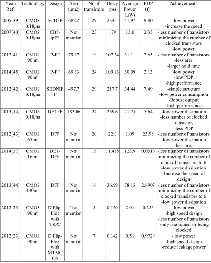
Performance comparisons among various CMOS FF based shift registers are shown in table 1. It was obtained that the efficiency of the FF can be assessed by calculating its number of transistors, area, average power, delay and PDP of the FF.
SCDFF is applied in reference [39] via Cross-coupled inverters to save the data at the output Q. However, problem is in the cross-coupled inverters that not only reduces the speed of discharging, but also bring about dissipation in short-circuit power. The period of the race current will be elongated when the capacitance of output load is large and can misrepresent the wanted output signal and
magnifies the dynamic power dissipation.
[image:3.612.102.280.246.544.2]313 signal from input source to the internal node of TSPC latch which reduce the transition time and improve speed and power. The static explicit-pulsed dual edge triggered Flip-flop (SEDNIFF) accompanies with latch node built-in is reported in reference [42]. A pulse generator circuit is implemented in SEDNIFF to make narrow pulses at the clock edges (rising and falling). The DETFF proposed in [14], is connected the parallel form of negative and positive latch. Tow inverter and one transmission gate connected back to back ,the output of two latch became input to 2:1 Mux by using one NMOS and one PMOS connected in series, the Mux was design and the gate derive by the inverted CLK. when the transmission gate is OFF the back to back connected inverters hold the data and to get the correct data at the output the Mux sends the latched data to the inverter in same time.. DETFF has less number of clocked transistors in comparison with FF [39-42]. The post layout experimental model results displays that proposed DETFF offers enhancement in power dissipation and PDP, but high delay compare with [39-42]. Consequently, the DETFF is very well matched for low power applications. Now design decreased the number of inverters and a new double edge triggered DFF is achieved in reference [43]. This design decreases four transistors. However, the number of clocked transistors rests as similar as before. The number of transistors needed to achieve the design 20 transistors. Designs in references [37], [44] are suggested to substitute the transmission gates by the n pass transistors. Essentially, n-type pass transistors offer weak high however, the n-type pass transistors are continued by an inverter, that along with a strong high. The number of transistor is reduced to 18 and 16 for the mentioned references, respectively while the number clocked transistors are just 6 transistors. The TSPC D-FF is proposed in [23]. The D-FF is made by applying two PMOS transistors and three NMOS transistors and with MTCMOS D-FF. MTCMOS D-FF is planned with seven transistors; two PMOS transistors, three NMOS, sleep and sleep bar that have more number of transistors but less power consumption. The malty threshold CMOS working with low and high threshold, when threshold is low it enhance the speed performance and when threshold is high it decrease the leakage power. This technology is decreasing power dissipation, propagates delay promotes.
All FF designs that have been discussed in table 1 can be applied in shift registers. The choice of the FFs design depends on the shift registers objective applications.
The basic types of shift registers are:
a.Serial In -Serial Out shift registers.
b.Serial In -Parallel Out shift registers.
c.Parallel In -Serial Out shift registers.
d.Parallel In- Parallel Out shift registers.
Serial In -Serial Out shift registers: The serial
in-serial out shift register receives data
consecutively, which is one bit at a time on a single line. It generates the kept data in serial form on its output as well. A basic 4-bit shift register is designed applying 4-D flip-flops, as displayed in Figure 6.
Figure 6: Serial in-serial out shift register [22].
[image:4.612.332.516.451.531.2]Serial In- Parallel Out shift registers : In this type of register data is received consecutively as like as discussed in the SISO section. Figure 18 displays the serial in parallel out diagram for this type of register. The variance is within the method that the data bits are derived of the register. When the information is kept, every bit get appear on its own output line, and concurrently whole bits are accessible.
Figure 7: Serial in - parallel out register [18]
[image:5.612.88.301.73.175.2]
314 Figure 8: Parallel in Serial out Shift Register [22]
Parallel in- Parallel out Shift Register: For the parallel in parallel out shift registers, whole data bits are sorted on the parallel outputs directly following the concurrent entry of the data bits. A design of a 4-bit parallel in - parallel out shift register by is illustrated in Figure 9. Inputs and outputs make the parallel operation. The clock is used to activate all the flip flops linked as depicted below. The D1, D2, D3 and D4 are the parallel inputs and the Q1, Q2, Q3 and Q4 are the parallel outputs. When the register is clocked, the whole data at the D's inputs get appear at the resultant Q’s outputs simultaneously.
Figure 9: Parallel in/out Shift Register [22]
Shift registers are used in many applications. Some of these applications are:
To produce time delay: the SISO shift register can be implemented as a time delay system [45- 46]. The amount of delay may be measured as either the number of flip-flops in the register or the frequency of the clock.
To simplify combinational logic: The main difficulty within the understanding of synchronous serial circuits is the duty of binary codes to the internal conditions of the circuit to decrease the convolution of needed circuits. Through assigning one FF to one internal state, it is probable to alleviate the combinational logic needed to understand the serial circuit. Once the circuit is in a specific condition, the flip-flop related to that condition is set to high and the rest flip-flops remain low [47].
To convert serial data to parallel data: A computer or microprocessor-based system usually needs input data to be in parallel format. Then commonly, these systems should connect to the external devices that send or receive serial data. Therefore, serial-to-parallel conversion is needed.
As displayed in earlier part, a serial in - parallel out register can attain this [48].
[image:5.612.330.515.279.422.2]In [37], the design of DETFF for shift registers for replacing the entire transmission gate in the conventional design by the n pass transistors. Mainly, n-type pass transistors result in weak high. However, the n-type pass transistors, which are accompanied by an inverter that gives strong high. Number of transistor is reduced to 18 where the clocked transistors are just 6 transistors. The shift registers are constructed using this DFF’s, thus all the performance parameters as well as Power consumption, area Delay are improved and the design is best appropriate for high speed and low power usages.
Figure 10: Proposed DETFF [37]
Design of 4-bit shift register (PIPO) by applying diverse design of FF (IP-DCOFF, SCCER FF, EPTL FF) was performed in [49]. Design FF with The enhanced pulse triggered low-power flip-flop (EPTLFF) decrease the discharging path and restricts pointless internal node transitions to decrease power consumption and delay. Therefore, this design of PIPO shift register applying EPTLFF is better than the other designs.
[image:5.612.110.288.337.434.2][image:6.612.262.519.64.296.2]
315 Figure 11: SISO Shift Register with ADOC &
RTPG [50]
Design and construction of low power single edge triggered D-FF based shift registers (SISO, SIPO, PISO and PIPO) was accomplished in [51]. D-FF design includes regenerative feedback just for slave, which increase the performance. Though in most projects master slave logic is applied and recreating feedback is favored for slave and master. This design is so consistent in comparison with other designs and can be applied for high speed usages. This design decreases the total area and
power consumption. This design is most
[image:6.612.115.282.407.509.2]appropriate for the low power usages.
Figure 12: Low power set D-FF [51]
The design of shift registers applying TSPC flip-flops (True Single Phase Clock) was presented in [52]. TSPC technique is added for designing D flip-flops. TSPC uses only a single clock and 2 or 3 clocked transistors in every latch without local inversion of the clock as such inversion needs additional clocked systems. Moreover uses OBSC (optimized bus specific clock gating). This technique is presented which reduces the problem of gated flip-flop choice by appropriate selection of subset of flip-flops. It may reduce dynamic power by 25.07%. Moreover, simulation results display that the recommended technique reaches 32% discount in active leakage power.
Figure 24: Proposed OBSC Circuit [52]
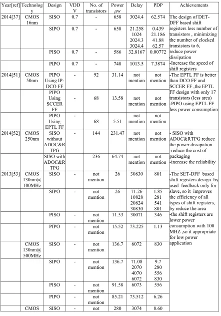
This review article was present a variety of low power and high efficiency shift registers published in different scientific papers. Table 2 displays summary of experimental outcomes for shift registers collected from different research papers. After reviewing it was found that the recent research on shift registers are mainly concentrating on average power, PDP, delay.
From the literature, it was found that the performance of shift registers could be accessed through measuring mean power, PDP and delay for shift registers. The Flip-flops (FFs) are the basic storage elements used widely in all types of shift registers. FFs contribute a chief part of the chip area and power consumption to the global system plan. The papers always tend to choose the simple
circuit structure of FFs due to its
uncomplicatedness and easy implementation (small area and less number of clocked transistors). Nevertheless, from the conductive literature review, it can be concluded that regularly there is a need to use the new technology in order to reduce the power consumption and to satisfy a low power, high performance for shift registers.
4. CONCLUSION
316 requires high performance of flip-flops because it has significant impact to the power consumption, which will degrade the performance of shift registers.
REFRENCES:
[1] T. Ravi and V. Kannan, “Effect of N-Type
Cntfet on Double Edge Triggered D Flip-Flop
Based PISO Shift Register”, in Proc. of
International Conference on Emerging Trends
in Science, Engineering and Technology, 13-14
Dec, 2012, pp. 344-349.
[2] E. Mollick, “Establishing Moore's law”, IEEE
Annals of the History of Computing, vol. 28, No. 3, 2006, pp. 62-75.
[3] D. E. Schwartz and T. N. Ng, “Comparison of
static and dynamic printed organic shift
registers”, IEEE Electron. Device Lett, vol. 34,
2013, p. 271-273.
[4] A. Sayed, H. Al-Asaad, “A New Low Power
High Performance Flip-Flop” IEEE Conference,
2006, pp 723-726.
[5] O. Sarbishei and M. Maymandi-Nejad, “A
novel overlap-based logic cell: An efficient implementation of flip–flops with embedded logic”, IEEE Transactions on Very Large Scale Integration (VLSI) Systems, vol. 18, No. 2, 2010, pp. 222-231.
[6] L. F. Rahman, M. B. I. Reaz, M. A. M. Ali, et
al., “Implementation of sense amplifier in 0.18-
µm CMOS process”, Elektronika ir
elektrotechnika (Electronics and Electrical Engineering), no. 4, 2012, pp. 113–116.
[7] Marufuzzaman, M.B.I Reaz, M.A.M. Ali,
"FPGA implementation of an intelligent current dq PI controller for FOC PMSM drive,"
International Conference on Computer
Applications and Industrial Electronics, 5-8 Dec, 2010, pp.602-605.
[8] M. Marufuzzaman, M. B. I. Reaz, M. A. M. Ali,
and L. F. Rahman, “Hardware approach of two way conversion of floating point to fixed point
for current dq PI controller of FOC PMSM
drive,” Electronics and Electrical Engineering,
vol. 7, no. 123, pp.79–82, 2012.
[9] 6] L. Rahman, M. B. I. Reaz, C. T. Gyu, and M.
Marufuzzaman, “Design of sense amplifier for non volatile memory,” Revue Roumaine Des Sciences Techniques, vol. 58, no. 2, 2013, pp. 173–182.
[10]N. Sklavos, P. Kitsos, N. Zervas, and O.
Koufopavlou, "A New Low Power and High
Speed Bidirectional Shift Register
Architecture," in International
Workshop-Power And Timing Modeling, Optimization and Simulation, 2001.
[11]Y. W. Kim, J. S. Kim, J. W. Kim, and B.-S.
Kong, "CMOS differential logic family with
conditional operation for low-power
application," IEEE Transactions on Circuits
and Systems II: Express Briefs, vol. 55, No. 5, 2008, pp. 437-441.
[12]P. Girard, "Low power testing of VLSI circuits:
Problems and solutions," in First International Symposium on Quality Electronic Design, March, 2000, pp. 173-179.
[13]N. Sirisantana, L. Wei, and K. Roy,
"High-performance low-power CMOS circuits using multiple channel length and multiple oxide thickness," in Int. Conf. on Computer Design, September, 2000, pp. 227-232.
[14]G. Singh and V. Sulochana, "Low Power Dual
Edge-Triggered Static D Flip-Flop," arXiv
preprint arXiv, 1307.3075, 2013.
[15]M. Nimbalkar and V. Pujari, "Design Of Low
Power Shift Register Using Implcit And Explicit Type Flip Flop." International Journal of VLSI and Embedded Systems, vol. 5, 2014, pp.1023-1027.
[16]Zhao, Peiyi, Tarek K. Darwish, and Magdy
Bayoumi. "High-performance and low-power
conditional discharge flip-flop." IEEE
Transactions on Very Large Scale Integration (VLSI) Systems, vol. 12, no. 5 2004,pp.477-484.
[17]S. Reddy and R. Dandapani, "Scan design using
standard flip-flops," IEEE Design & Test of Computers, vol. 4, 1987, pp. 52-54.
[18]H. Mahmoodi, V. Tirumalashetty, M. Cooke, K.
Roy, “Ultra low-power clocking scheme using
energy recovery and clock gating”, IEEE
transactions on very large scale integration (VLSI) systems, vol. 17, No. 1, 2009, p. 33-44.
[19]H. Kawaguchi and T. Sakurai, “A reduced
clock-swing flip-flop (RCSFF) for 63% power
reduction”, IEEE Journal of Solid-State
Circuits, vol. 33, No. 5, 1998, pp. 807-811.
[20]C. K. Teh, T. Fujita, H. Hara, and M. Hamada,
“A 77% energy-saving 22-transistor
single-phase-clocking D-flip-flop with
adaptive-coupling configuration in 40nm CMOS”, in
IEEE Solid-State Circuits Conference Digest of Technical Papers (ISSCC), 20-24 Feb. 2011, pp. 338-340.
[21]T. L. Floyd, Digital Fundamentals, 10/e.
317
[22]M. Arunlakshman, T. Dineshkumar, and N.
Mathan, “Performance Evaluation of 6
Transistor D-Flip Flop based Shift Registers
using GDI Technique”, International Journal
of Advanced Research in Computer and Communication Engineering, vol. 3, No. 3, 2014, pp.5858-5861.
[23]D. Sagar and T. K. Moorthy, “Design of a Low
Power Flip-Flop Using MTCMOS Technique”, International Journal of Computer Applications and Information Technology, vol. 1, No. 1, 2012, pp. 19-21.
[24]S. Mishra, S. Rofail, and K. Yeo, “Design of
high performance double edge-triggered
flip-flops”, IEE Proceedings of Circuits, Devices
and Systems, Vol. 147. No. 5. IET, 2000, pp. 283-290.
[25]T. D. Loveless, S. Jagannathan, T. Reece, J.
Chetia, B. L. Bhuva, M. W. McCurdy, L. W. Massengill, S-J. Wen, R. Wong and D. Rennie, “"Neutron-and proton-induced single event upsets for D-and DICE-flip/flop designs at a 40
nm technology node”, IEEE Transactions on
Nuclear Science, vol. 58, No. 3, 2011, pp. 1008-1014.
[26]J. M. Hutson, V. Ramachandran, B. L. Bhuva,
X. Zhu, R. D. Schrimpf, O. A. Amusan, and L. M. Massengill, “Single event-induced error propagation through nominally-off transmission
gates”, IEEE Transactions on Nuclear Science,
vol. 53,No. 6, 2006, pp. 3558-3562.
[27]I. A. Khan and M. T. Beg, “A New Area and
Power Efficient Single Edge Triggered Flip-Flop Structure for Low Data Activity and High
Frequency Applications”, Innovative Systems
Design and Engineering, vol. 4, no. 1, 2013, pp. 1-12.
[28]X. Wang and W. H. Robinson, “A low-power
double edge-triggered flip-flop with
transmission gates and clock gating”, in IEEE
International Midwest Symposium on Circuits and Systems, 1-4 Aug. 2010, pp. 205-208.
[29]M. Sharma, A. Noor, S. C. Tiwari, and K.
Singh, “An area and power efficient design of
single edge triggered D-flip flop” in IEEE
International Conference on Advances in Recent Technologies in Communication and
Computing, 27-28 Oct. 2009, pp. 478-481.
[30]M. Marufuzzaman, H. N. B. Rosly, M. B. I.
Reaz, L. F. Rahman, and H. Hussain. “Design of Low Power Linear Feedback Shift Register”, Journal of Theoretical & Applied Information Technology Vol. 61, no. 2, 2014, pp. 326-333.
[31]H. Thapliyal, N. Ranganathan, and S. Kotiyal,
“Design of testable reversible sequential
circuits”, IEEE Transactions on Very Large
Scale Integration Systems, vol. 21, no. 7, 2013, pp. 1201-1209.
[32]Z. Peiyi, J. McNeely, P. Golconda, M.
Bayoumi, R. Barcenas, and W. Kuang, “Low-power clock branch sharing double-edge
triggered flip-flop”, IEEE Transactions on Very
Large Scale Integration (VLSI) Systems, Vol. 15, no. 3, 2007, pp. 338-345.
[33]A. Gago, R. Escano, and J. A. Hidalgo.
“Reduced implementation of D-type DET
flip-flops”, IEEE Journal of Solid-State Circuits,
Vol. 28, no. 3, 1993, pp.400-402.
[34]A. Strollo, E. Napoli, and C. Cimino, “Low
power double edge-triggered flip-flop using one
latch”, Electronics Letters, vol. 35, No. 3, 1999,
pp. 187-187.
[35]X. Wang and W. H. Robinson, “Asynchronous
Data Sampling Within Clock-Gated Double
Edge-Triggered Flip-Flops”, IEEE Transactions
on Circuits and Systems I: Regular Papers, vol. 60,No. 9, 2013, pp.2401-2410.
[36]T. Ravi and V. Kannan, “Effect of N-type
CNTFET on Double edge triggered D flip-flop
based PISO shift register”, IEEE International
Conference on Emerging Trends in Science,
Engineering and Technology, 13-14 Dec. 2012,
pp. 344-349.
[37]M. Arunlakshman, “Power and delay analysis
of double edge triggered D-Flip Flop based shift
registers in 16nm MOSFET technology” Int.
Journal of Advanced Research in Electrical, Electronics and Instrumentation Engg., vol. 3, No. 4, 2014, pp. 8560-8568.
[38]W. Chung, T. Lo, and M. Sachdev, “A
comparative analysis of low-power low-voltage
dual-edge-triggered flip-flops”, IEEE
transactions on very large scale integration (VLSI) systems, vol. 10, No. 6, 2002, pp. 913-918.
[39]M-W. Phyu, W. L. Goh, and K-S. Yeo. “A
low-power static dual edge-triggered flip-flop using an output-controlled discharge configuration”, in IEEE International Symposium on Circuits
and Systems, May 2005, pp. 2429-2432.
[40]P. Zhao, J. McNeely, P. Golconda, M.
Bayoumi, R. Barcenas, and W. Kuang, “Low-power clock branch sharing double-edge
triggered flip-flop”, IEEE Transactions on Very
318
[41]Y.-T. Hwang, J.-F. Lin, and M.-H. Sheu,
“Low-power pulse-triggered flip-flop design with
conditional pulse-enhancement scheme”, IEEE
Transactions on Very Large Scale Integration (VLSI) Systems, vol. 20, No.2, 2012, pp. 361-366.
[42]X.-X. Wu and J.-Z. Shen, “Low-power
explicit-pulsed triggered flip-flop with robust output”, Electronics Letters, vol. 48, No. 24, 2012, pp. 1523-1525.
[43]I. A. Khan, D. Shaikh, and M. T. Beg, “2 GHz
low power double edge triggered flip-flop in
65nm CMOS technology”, in IEEE
International Conference on Signal Processing,
Computing and Control, March 2012, pp. 1-5.
[44]T. Ravi, D. Irudaya Praveen and V. Kannan,
“Design and Analysis of High Performance
Double Edge Triggered D-Flip Flop”,
International Journal of Recent Technology and Engineering, vol.1, No. 6, 2013, pp. 15-18.
[45]J.-F. Lin, “Low-Power Pulse-Triggered
Flip-Flop Design Based on a Signal Feed-Through
Scheme”, IEEE Transaction on Very Large
Scale Integration (VLSI) System, vol. 22, No. 1, 2014,pp.181-185.
[46]L. Lee, S. Al-Sarawi, and D. Abbott, “Low
power serial-parallel dynamic shift register”, Electronics Letters, vol. 39, No. 1, 2003, pp. 19-20.
[47]I. Pomeranz and S. M. Reddy, “3-weight
pseudo-random test generation based on a deterministic test set for combinational and
sequential circuits”, IEEE Transactions on
Computer-Aided Design of Integrated Circuits and Systems, vol. 12, No. 7, 1993, pp. 1050-1058.
[48]S. I. Kartashev, “A Microcomputer with a
Shift-Register Memory”, IEEE Trans. on Computers,
vol. 100, No. 5, 1976, pp. 470-484.
[49]T. Ravi, and V. Kannan, “High Performance
Double Edge Triggered D Flip-Flop Based Shift
Registers Using CNTFET”, IUP Journal of
Electrical and Electronics Engineering, vol. 7, no. 1 2014, pp. 19.
[50]K. Aditya, B. B. Kotaru, and B. B. Naik,
“Design of low power shift register using activity-driven optimized clock gating and
run-time power gating”, in IEEE International
Conference on Green Computing
Communication and Electrical Engineering,
Mar. 2014, pp. 1-7.
[51]N. Mathan, T. Ravi, E. Logashanmugam,
“Design And Analysis Of Low Power Single
Edge Triggered D Flip Flop” International
journal of Advanced Research in Computer Science and Electronics Engineering, vol. 2, No. 2, 2013, pp.2-6.
[52]R. Rampriya, T. Marutharaj, "Power Efficient
Design of Sequential Circuits using OBSC and
RTPG Integration," International Journal of
Computer Science and Mobile Computing, vol. 2, No. 9, 2013, pp.268-278.
[image:10.612.89.522.115.655.2]
319
Table 1: Performance Comparison Among Various Design Of CMOS FF For Shift Registers
Year/ Ref.
Technology Design Area
(μm2)
No of transistors
Delay (ps)
Average Power
(μW)
PDP (fj)
Achievements
2005[39] CMOS
0.18μm
SCDFF 682.2 29 234.5 41.97 9.80 -low power
-increase the speed
2007[40] CMOS
0.18μm
CBS-ipFF
Not mention
23 179 13.0 2.33 -less number of transistors
-minimizing the number of clocked transistors
-low power
2012[41] CMOS
90nm
P-FF 79.17 19 107.24 31.11 2.65 -less number of transistors
-less area -larger hold time
2014[45] CMOS
90nm
P-FF 69.13 24 109.13 30.09 2.13 -low power
-low PDP -high performance
2012[42] CMOS
0.18μm
SEDNIF F
497.7 29 217.7 34.44 7.49 -simple structure
-low power consumption -Robust out put -high performance
2013[14] CMOS
0.18μm
DETFF 183.06 24 259.6 21.75 5.64 -low power dissipation
-less number of clocked transistors -less PDP
2012[43] CMOS
65nm
DFF Not
mention
20 22.0 1.09 23.98 -less number of transistors
-low power dissipation -less area
2014[37] CMOS
16nm
DET-DFF
Not mention
18 11.418 123.9 0.0516 -less number of transistors
-minimizing the number of clocked transistors to 6 -low power dissipation -Increase the speed of
design
2013[44] CMOS
130nm
DFF Not
mention
16 36.99 78.15 2.8907 -less number of transistors
-minimizing the number of clocked transistors to 6 -low power dissipation
2012[23] CMOS
90nm
D Flip-Flop with TSPC
Not mention
5 0.126 2.01 0.253 -low power
-high speed design -less number of transistors
-only one transistor being clocked
2012[23] CMOS
90nm
D Flip-Flop with MTMC
OS
Not mention
7 0.142 0.51 0.9729 - low power
[image:11.612.87.529.110.741.2]
320
Table 2: Performance Comparison Among Various Designs Of Shift Registers
Year[ref] Technolog y
Design VDD
V
No. of transistors
Power μw
Delay PDP Achievements
2014[37] CMOS 16nm
SISO 0.7 - 658 3024.4 62.574 The design of
DET-DFF based shift registers less number of transistors , minimizing the number of clocked transistors to 6, reduce power dissipation
-Increase the speed of shift registers
SIPO 0.7 - 658 21.258
1024 2024.3 3024.4 0.439 21.186 41.88 62.57
PISO 0.7 - 586 32.8167 0.00772
PIPO 0.7 - 748 1013.5 7.3874
2014[51] CMOS 50nm
PIPO Using
IP-DCO FF
- 92 31.14 not
mention not mention
-The EPTL FF is better than DCO FF and SCCER FF ,the EPTL FF design with only 17 transistors (less area) -PIPO using EPTL FF less power consumption PIPO
Using SCCER
FF
- 68 13.58 not
mention not mention PIPO Using EPTL FF -
68 5.51
not mention
not mention
2014[52] CMOS 250nm
SISO without ADOC&R
TPG
- 144 231.47 not
mention not mention
- SISO with
ADOC&RTPG reduce the power dissipation -reduce the cost of packaging
-increase the reliability SISO with
ADOC&R TPG
236 64.74 not
mention not mention
2013[53] CMOS 130nm@ 100MHz
SISO - not
mention
26 30830 801 -The SET-DFF based
shift registers design by used feedback only for slave, so it improves the efficiency of all types of shift registers, by reduce the area -the shift registers are lower power
consumption with 100 MHZ ,so it appropriate for low power
application
SIPO - not
mention
26 71.26
10828 20824 30830 1.85 281 541 801
PISO - not
mention
11.53 30071 346
PIPO - not
mention
15.52 73.225 1.13
CMOS 130nm@ 500MHz
SISO - not
mention
136.7 6072 830
SIPO - not
mention
136.7 71.08
2070 4070 6072 9.7 280 556 830
PISO - not
mention
91.58 6073 556
PIPO - not
mention
85.21 73.512 6.26
321 130nm@
1GHz
mention
SIPO - not
mention
280 71.226
1071 2071.8
3074
19.9 299 580 860
PISO - not
mention
202.3 3073 621
PIPO - not
mention
177.1 74.733 13.2
2013[54] CMOS 90nm@
1GHz
SISO 1 not
mention
79.442 153 12.1546 -The design of FF based
shift registers reduce the leakage power
-low delay -low PDP
SIPO 1 not
mention
79.442 51 4.05154
PISO 1 not
mention
162.098 213 34.5268
PIPO 1 not
mention
![Figure 3: D Flip Flop Transmission gates [28].](https://thumb-us.123doks.com/thumbv2/123dok_us/8910105.958839/2.612.323.520.337.448/figure-d-flip-flop-transmission-gates.webp)
![Figure 5: (a) General diagram of DETFF [36]. (b) Conventional DETFF [37].](https://thumb-us.123doks.com/thumbv2/123dok_us/8910105.958839/3.612.102.280.246.544/figure-a-general-diagram-of-detff-conventional-detff.webp)
![Figure 7: Serial in - parallel out register [18]](https://thumb-us.123doks.com/thumbv2/123dok_us/8910105.958839/4.612.332.516.451.531/figure-serial-in-parallel-out-register.webp)
![Figure 8: Parallel in Serial out Shift Register [22]](https://thumb-us.123doks.com/thumbv2/123dok_us/8910105.958839/5.612.330.515.279.422/figure-parallel-serial-shift-register.webp)
![Figure 12: Low power set D-FF [51]](https://thumb-us.123doks.com/thumbv2/123dok_us/8910105.958839/6.612.115.282.407.509/figure-low-power-set-d-ff.webp)