http://dx.doi.org/10.4236/jsip.2015.62005
Comparative Study and Analysis of
Performances among RNS, DBNS, TBNS and
MNS for DSP Applications
Rakhi Roy1, Debanjana Datta2, Somnath Bhagat3, Sangita Saha3, Amitabha Sinha3 1Neotia Institute of Technology Management and Science, Diamond Harbour, West Bengal, India 2Savita Devi Education Trust-Brainware Group of Institutions, North 24 Pgs, West Bengal, India 3School of Engineering and Technology, West Bengal University of Technology, Salt Lake, India Email: [email protected], [email protected], [email protected],
[email protected], [email protected]
Received 22 February 2015; accepted 25 March 2015; published 27 March 2015
Copyright © 2015 by authors and Scientific Research Publishing Inc.
This work is licensed under the Creative Commons Attribution International License (CC BY).
http://creativecommons.org/licenses/by/4.0/
Abstract
This paper presents a comparative study of the performances of arithmetic units, based on differ-ent number systems like Residue Number System (RNS), Double Base Number System (DBNS), Tri- ple Base Number System (TBNS) and Mixed Number System (MNS) for DSP applications. The per-formance analysis is carried out in terms of the hardware utilization, timing complexity and effi-ciency. The arithmetic units based on these number systems were employed in designing various modulation schemes like Binary Frequency Shift Keying (BFSK) modulator/demodulator. The anal-ysis of the performance of the proposed modulator on above mentioned number systems indicates the superiority of other number systems over binary number system.
Keywords
Residue Number System (RNS), Double Base Number System (DBNS), Triple Base Number System (TBNS), Mixed Number System (MNS), Look Up Table (LUT), Digital Signal Processing (DSP)
1. Introduction
To evaluate this carry chain and have a carry free operation residue number system came into popularity.
Re-sidue Number System (RNS) [1] [2] is an un-weighted number system which supports carry-free addition,
bor-row-free subtraction, and single step multiplication without any partial products. With residue number system computation time is highly reduced as a result of high speed real time operations being achieved. In residue number system as addition and multiplication are performed individually on each digit, the arithmetic operations become faster.
In Double Base Number System (DBNS) [3]-[6] any number is represented as a power of 2 and 3. During any
arithmetic operation these powers only participate in the execution, eliminating partial products of binary mul-tiplication. So, processing becomes faster.
Triple Base Number System (TBNS) [7] [8] is an improvement over DBNS, requiring smaller number of
multipliers and adders for multiplication but at the cost of greater computational complexity. The conversion stages in TBNS are much more complex compared with DBNS, but execution time is greatly reduced, resulting in high speed multiplication.
Mixed Number System (MNS) [9] [10] employs both residue and double base number systems. It uses RNS
adder and DBNS multiplier together to utilize both their advantages. It provides more speed of execution than any other number system but suffers from overheads like three conversion stages for being implemented.
2. Review of Residue Number System
In residue number system [1] [2], a number is represented by several residue digits. Addition and multiplication operations are performed independently on each residue. As a result high degree of concurrency can be achieved. RNS arithmetic uses a set of numbers
(
x x x1, , , ,2 3 xn)
which evaluates a number X using a set of integers(
m m m1, , , ,2 3 mp)
called moduli. These moduli are pair wise relatively prime to each other, i.e. GCD(xi, xj) = 1.Now if M be the dynamic range (where X < M) then,
1 2 3 n
M m m m= × × × × m .
and the residue are given as,
mod
i i
x =X m
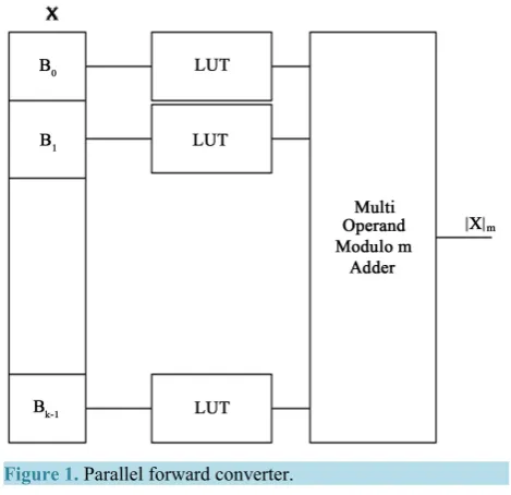
2.1. Forward Converter
In this paper, the forward converter [2] has been designed using partition method. In this method the binary number is first partitioned in k blocks having p bit each, where partitions are represented as Bk−1,Bk−2, , , B B1 0,
The number can be expressed in terms of the partitions as,
1 02 k jB j j
X − B
=
=
∑
1 1
02 02
k k
jB jB
j j
m j j m
m m
X − B − B
= =
=
∑
=∑
where m is the modulus. Now this equation is implemented by storing all the possible values of 2jB j m
B di-
rectly in LUT’s whose locations are accessed by the value of Bj. the size of the LUT is given by (p × log2m)
where p is the number of bits in each block. As it is a parallel converter it will require k number of LUT’s for every moduli followed by a multi operand modulo adder which will add the output bits from the k LUT’s. As a result of these parallel operations, this method of forward conversion is faster compared to other means of con-version.
Figure 1. Parallel forward converter.
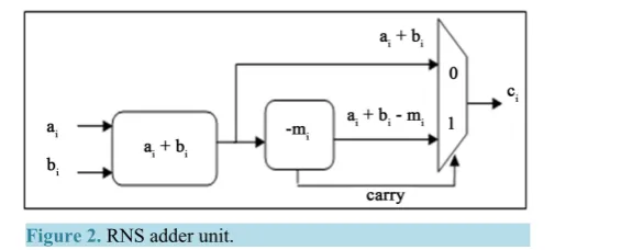
2.2. Modulo Adder
In Residue Number System, addition [1] is done by adding each residue individually which eradicates the delay for carry. Addition operation is done by decomposing it into a set of parallel sub additions. Now if xi and yi be
the inputs to a RNS adder and zi be their output result then it can be mathematically expressed as,
(
)
mod ,i i i i
z = x y+ m
where 0<x yi, i<mi−1. While implementing RNS adder the above equation can be evaluated as, when
i i i i i i
z = +x y x y+ <m
when
i i i i i i i
z = + −x y m x y+ >m
Several architectures have been proposed for implementing modulo addition on the basis of these equations. A simple modulo adder is given here (Figure2) using simple ripple carry adder (RCA), a subtractor and a 2to1 mux.
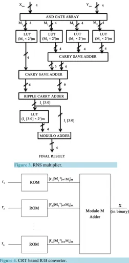
2.3. Modulo Multiplier
RNS multiplication [11] uses a combination of LUT’s and arithmetic units keeping in mind the balance between speed and hardware complexity. Multiplication has been done using an AND gate array, some LUT’s and using a multistage carry save adder known as the Wallace Tree Multiplier. The two inputs xrns and yrns are applied to
the inputs of the array of AND gates which generate the partial products. The sum of partial products is given mathematically as,
( )
[ ]
1
0
i n
k mi k rns rns
i M M x y k
= −
=
= ×
∑
where Mk is the partial product which is given as
[ ]
k rns rns
M =x ×y k
Now after the bit by bit multiplication using and gate arrays the partial products are stored in the LUT’s in the form of
( )
(
2k)
k mi k mi
M = M ×
Figure 2. RNS adder unit.
then added with the other bits to generate the final multiplication result. The LUT contains the mapping function given as,
[ ]
(
Ir 5 : 4 2k)
mi ×where Ir is the 6 bit output of the Wallace tree multiplier unit. The architecture of the proposed architecture is given in Figure3.
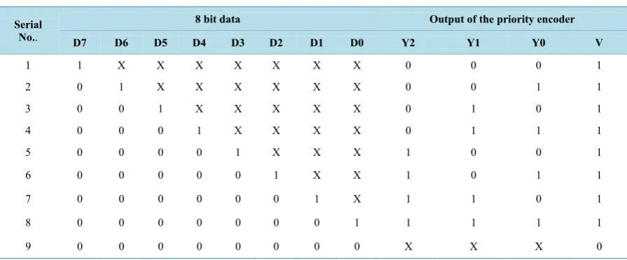
2.4. Reverse Converter
Reverse conversion [2] [12] is implemented using the Chinese Remainder theorem. It is implemented in parallel, meeting our requirement for high speed applications. Here the reverse conversion is done purely depending on LUT approach where the output of LUT’s is added to get the final result. Residue inputs of different moduli
individually are applied as for addressing the LUT’s which generate, 1
n n n n M
r M m M−
as the output, where M is the range of the residue digits. The outputs are then added by a modulo M adder to get the converted binary output. The results lie within the range M (Figure 4).
3. Review of DBNS Theory and Analysis
Double Base Number System [3]-[6] is a special way of representing integers as a sum of mixed power of two
(2) and three (3). This number representation scheme is unusually sparse, which is a good measure for potential applications. In DBNS, we represent integers in the form of the following equation
( )i j, i j, 2 3 wherei j i j,
{ }
0,1x=
∑
d d =Therefore, binary system is special case of above representation. From these expression it is clear that when a binary number is converted into double base number system (DBNS), it is represented as number consisting of several (i, j) pairs. These (i, j) pairs are known as DBNS indices.Figure5 depicts a DBNS table where i and j both are the range from 0 to 3.
Greedy algorithm is an iterative approach for computing these indices. Since each iteration finds one index, the number of iterations indicates the number of one’s (1) in the DBNS table which are often referred to as ac-tive cells. The values given in each box in the DBNS table indicate the weight for the corresponding acac-tive cell.
The maximum decimal number which is represented by a DBNS system with m × n cells can be obtained by
adding the weights of all the m × n cells. Hence we can conclude that using a 4 × 4 DBNS table maximum de-cimal number that can be represented is 600 in followingFigure 5.
3.1. Conversion of Binary to DBNS
The conversion of binary to DBNS [13] [14] means extracting the indices, i.e. (i, j) pairs, that represent the number. Look-up tables (LUT) [5] [15] are used for the conversion of the numbers where dynamic range is not large. When the dynamic range increases, LUT based approach becomes inefficient because of exponential in-crease in LUT size.
To implement binary to DBNS conversion different approaches are used like Binary Search Tree (BST) [14]
Range Table Search (RTS) [15], Improved Range Table Search (IRTS) [13], etc. Among all these approaches
Figure 3. RNS multiplier.
Figure 4. CRT based R/B converter.
3.1.1. Improved Range Table Search
Improved Range Table Search (IRTS) [13] is the improved version of Range Table Search (RTS) approach. The
architecture that represents IRTS conversion approach has been described below. To implement this architecture Table 1 has been deployed.
3.1.2. Algorithm of the Architecture
a) First the data is passed through the 8:3 priority encoder, whose inputs are D7-D0 and outputs are Y2-Y0 and V (valid bit);
b) The three bit output is sent to control signal generation unit which checks the condition;
c) The control signal generation unit then send appropriate number to compare with the incoming data; d) The hybrid approach has been used here for the functioning of control signal unit.
3.1.3. Architecture of the Converter
[image:6.595.150.451.310.499.2]Architecture [13] of the above algorithm is shown inFigure6. For example, a binary number (X) is encountered by the Processing Element (PE) for which D7 = 0 & D6 = 1, so the number is in between 63 and 128. So, the output of the encoder is 001 and V = 1. The control signal generation unit checks the encoder output and sends 72 to the input of the comparator for 1st comparison and 54 and 108 to the input of the output multiplexer. If X > 72 then lower input of the multiplexer is enabled and X is compared to the 108. If X > 108, then the co-ordinate
Figure 6. Architecture of Processing Element (PE).
Table 1. Input and output of the priority encoder.
Serial No..
8 bit data Output of the priority encoder
D7 D6 D5 D4 D3 D2 D1 D0 Y2 Y1 Y0 V
1 1 X X X X X X X 0 0 0 1
2 0 1 X X X X X X 0 0 1 1
3 0 0 1 X X X X X 0 1 0 1
4 0 0 0 1 X X X X 0 1 1 1
5 0 0 0 0 1 X X X 1 0 0 1
6 0 0 0 0 0 1 X X 1 0 1 1
7 0 0 0 0 0 0 1 X 1 1 0 1
8 0 0 0 0 0 0 0 1 1 1 1 1
[image:6.595.90.538.535.721.2]of 108 is the 1st pair of the (i, j) for X. If X < 72 in the 1st comparison, then the upper input of the multiplexer is enable and X is compared to the 54, i.e. 1st pair of (i, j) will be the co-ordinate of 54 or 72.
So, here at least and at most two comparisons are required for extracting the indices means (i, j) pairs. Then the subtraction is done and the result is sent to the next PE. If zero is encountered, it is easily checked by the va-lid bit of priority encoder. No additional circuitry is required for this problem.
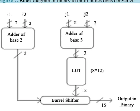
It is approved that for 4 × 4 DBNS table that the maximum five (5) number or (i, j) pairs are needed to represent an 8-bit binary number. So, a maximum of five Processing Element (PE) are employed which are con- nected in cascade. The block diagram of such a configuration is shown in Figure 7.
When the first binary data enters into the stage one of the Binary to DBNS Converter, maximum 5 cycles will be required to extract the (i, j) pairs. When the partial conversion data for the first input data enters into the second stage, the second input binary data enters into the first stage of the pipeline and so on. So, after 5 clock cycle each binary data will effectively take 1 clock cycle to represent the corresponding DBNS based number.
3.2. DBNS Multiplier
DBNS multiplication [13] [14] [16] [17] operation can be done after converting the binary number to DBNS.
The extracted indices (i, j pairs) are used in the multiplication. Since i, j pairs are in binary form, the multiplica-tion of DBNS is done by adding the i, j pairs in powers of 2 and 3. So, the complexity of the multiplication is reduced. This gives a great advantage in DBNS multiplication as compared to binary multiplication.
Multiplication of two DBNS numbers are expressed as the following equation
(
2 3i1 ji) (
2 3i2 j2)
2i i1 2 3j1 2jX Y× = ⋅ × ⋅ = + ⋅ +
Two perform the above operation two Adders, one Look Up Table (LUT), one Barrel Shifter are required. One adder is performing the addition of indices on base 2 and another adder is performing the addition of indic-es on base 3. The binary equivalent of 3b1+ b2 is then stored in the LUT. Then the data is passed through the barrel
shifter with the help of the first addition result. How many bits will be shifted is decided by the number of bits of the first addition result.
[image:7.595.175.419.430.506.2]The architecture to perform the task of the above expression is shown in Figure 8.
Figure 7. Block diagram of binary to multi indies dbns converter.
[image:7.595.177.419.516.707.2]DBNS Multiplier Structure
Let us take two binary numbers K and L. After converting them into DBNS they can be expressed as,
1 1 2 2 3 3 4 4 5 5
2 3i j 2 3i j 2 3i j 2 3i j 2 3i j
K= ⋅ + ⋅ + ⋅ + ⋅ + ⋅
1 1 2 2 3 3 4 4 5 5
2 3m n 2m 3n 2m 3n 2m 3n 2m 3n
L= ⋅ + ⋅ + ⋅ + ⋅ + ⋅
Now, when they are multiplied the result can be written as,
(
)
(
)
(
)
(
)
1 1 2 2 3 3 4 4 5 5
1 1 2 2 3 3 4 4 5 5
1 1 1 1 2 2 3 3 4 4 5 5
2 2 1 1 2 2 3 3 4 4 5 5
3 3 1
2 .3 2 3 2 3 2 3 2 3
2 3 2 3 2 3 2 3 2 3
2 3 2 3 2 3 2 3 2 3 2 3
2 3 2 3 2 3 2 3 2 3 2 3
2 3 2
i j i j i j i j i j
m n m n m n m n m n
i j m n m n m n m n m n
i j m n m n m n m n m n
i j m
K L× = + ⋅ + ⋅ + ⋅ + ⋅
× ⋅ + ⋅ + ⋅ + ⋅ + ⋅ = ⋅ × ⋅ + ⋅ + ⋅ + ⋅ + ⋅ + ⋅ × ⋅ + ⋅ + ⋅ + ⋅ + ⋅ + ⋅ ×
(
)
(
)
(
)
1 2 2 3 3 4 4 5 5
4 4 1 1 2 2 3 3 4 4 5 5
5 5 1 1 2 2 3 3 4 4 5 5
3 2 3 2 3 2 3 2 3
2 3 2 3 2 3 2 3 2 3 2 3
2 3 2 3 2 3 2 3 2 3 2 3
n m n m n m n m n
i j m n m n m n m n m n
i j m n m n m n m n m n
⋅ + ⋅ + ⋅ + ⋅ + ⋅ + ⋅ × ⋅ + ⋅ + ⋅ + ⋅ + ⋅ + ⋅ × ⋅ + ⋅ + ⋅ + ⋅ + ⋅ (15)
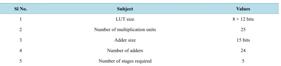
From the expression it is clear that each term in the DBNS expression of one number has to be multiplied with each term of the 2nd number. After that the multiplication results are added together to get the final result. For implementing these two stages are required: 1) multiplication stage; 2) addition stage. In multiplication stage 25 multipliers are required which produces 25 multiplication results. They are stored in the LUT locations. This block diagram of this multiplication stage is shown in Figure 9.
Because 25 multipliers are required in the previous stage, 25 outputs are generated. These 25 outputs are added using 24 adders in 5 stages as shown in Figure 10.
[image:8.595.128.479.98.314.2]The hardware requirements for implementing DBNS multiplier are summarized in Table 2.
Figure 9. DBNS multiplier (multiplication stage).
Table 2. Data corresponding to DBNS multiplier.
Sl No. Subject Values
1 LUT size 8 × 12 bits
2 Number of multiplication units 25
3 Adder size 15 bits
4 Number of adders 24
[image:8.595.90.542.612.719.2]Figure 10. DBNS multiplier (addition stage).
4. Review of TBNS Theory and Analysis
The Triple Base Number System (TBNS) [7] [8] is a special way of representing numbers as a sum of mixed
power of two (2), three (3), five (5). In TBNS, an integer is represented in the following way
{ }
, , , ,
, ,
2 3 5i j k where 0,1
i j k i j k
i j k
X =
∑
d d =It is clear that when j = k = 0, the number system represented binary number system. The TBNS can be con-sidered as a three dimensional geometric representation which is suitable to implement FIR, DFT, linear convo-lution etc of a signal with less hardware and design complexity. TBNS can perform arithmetic, using logarith-mic-like computational unit. The structure of a TBNS table where i, j, and k varies from 0 to 3 is more like a (4 × 4 × 4) cube which represent maximum decimal number up to 27,000. The TBNS table where i, j, and k varies from 0 to 3 is as follows (Table 3).
4.1. Conversion of Binary to Triple Base Numbers
Conversion of a number from its binary to TBNS [7] from aims at extracting the indices [(i, j, k) pairs] that are required to represent the number.
4.1.1. Conversion Using “Improved Range Table Search (IRTS)” Approach
Here IRTS [7] [13] approach has been followed which improves Range Table Search (RTS) for conversion of a
binary number to its corresponding three integer form (Table 4).
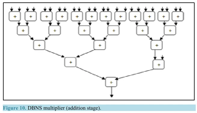
4.1.2. Architecture of Conversion Processing Element (CPE)
The Architecture of the CPE is described as an algorithm described (Figure 11).
a)First the data is passed through an 8:3 priority encoder, whose input are (D7-D0) and outputs are Y2, Y1, Y0 and v (valid bit);
b) Control Signal Generation Unit (CSGU) checks the priority encoder output; c) Coordinate of Comparator Cum Substractor (CCS) will be the first pair of (i, j, k);
d) Control signal generation unit send value to the input of CCS and comparison is done. The same method mentioned in the previous step is repeated;
e) If the process does not satisfy, then second set of values are sent in CSGU;
f) Here at least one and at most six comparisons are required to extract pair of (i, j, k); g) Then the subtraction is done and results are sent to the next CPE (Table 5).
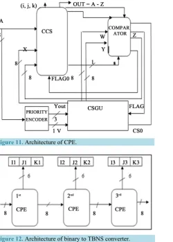
4.1.3. Architecture of Binary to Multiterm TBNS Converter
Maximum of three conversion processing elements (CPE) are required which are connected in cascade, i.e.
Figure 11. Architecture of CPE.
[image:10.595.91.540.464.720.2]Figure 12. Architecture of binary to TBNS converter.
Table 3. TBNS table for ranging from 0 to 3.
(i, j) co-ordinates N = 2i3j k = 0 k = 1 k = 2 k = 3
N × 5k N × 5k N × 5k N × 5k
(0, 0) 1 1 5 25 125
(1, 0) 2 2 10 50 250
(0, 1) 3 3 15 75 375
(2, 0) 4 4 20 100 500
(1, 1) 6 6 30 150 750
(3, 0) 8 8 40 200 1000
(0, 2) 9 9 45 225 1125
(2, 1) 12 12 60 300 1500
(1, 2) 18 18 90 450 2250
(3, 1) 24 24 120 600 3000
(0, 3) 27 27 135 675 3375
(2, 2) 36 36 180 900 4500
(1, 3) 54 54 270 1350 6750
(3, 2) 72 72 360 1800 9000
(2, 3) 108 108 540 2700 13,500
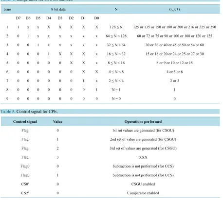
Table 4. Range table for an 8 bit number.
Srno 8 bit data N (i, j, k)
D7 D6 D5 D4 D3 D2 D1 D0
1 1 x x X X X X X 128 ≤ N 125 or 135 or 150 or 180 or 200 or 216 or 225 or 250 2 0 1 x x x x x x 64 ≤ N < 128 60 or 72 or 75 or 90 or 100 or 108 or 120 or 125 3 0 0 1 x x x x x 32 ≤ N < 64 30 or 36 or 40 or 45 or 50 or 54 or 60 4 0 0 0 1 X X X x 16 ≤ N < 32 15 or 18 or 20 or 24 or 25 or 27 or 30
5 0 0 0 0 0 X X x 8 ≤ N < 16 8 or 9 or 10 or 12 or 15
6 0 0 0 0 0 0 X X 4 ≤ N < 8 4 or 5 or 6
7 0 0 0 0 0 0 1 x 2 ≤ N < 4 2 or 3
8 0 0 0 0 0 0 0 1 N = 1 1
9 0 0 0 0 0 0 0 0 N = 0 0
Table 5. Control signal for CPE.
Control signal Value Operations performed
Flag 0 1st set values are generated (for CSGU)
Flag 1 2nd set of value are generated (for CSGU)
Flag 2 3rd set of values are generated (for CSGU)
Flag 3 XXX
Flag0 0 Subtraction is not performed (for CCS)
Flag0 1 Subtraction is not performed (for CCS)
CS0' 0 CSGU enabled
CS2' 0 Comparator enabled
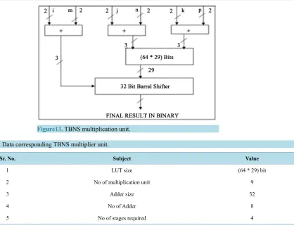
4.2. TBNS Multiplication Unit
After converting a given binary number to TBNS, we have to perform TBNS addition & multiplication [17] be-cause these two operations are primary in any digital signal processing system. The [i, j, k] pairs extracted at the time of conversion are used for addition and multiplication in TBNS. Since the extracted [i, j, k] pairs are in bi-nary form, the addition in TBNS will give no advantages as compared to bibi-nary addition. So bibi-nary addition performed.
But as TBNS multiplication is concerned, the [i, j, k] pairs will be added in powers of 2, 3 & 5. So, naturally the complexity of multiplication is reduced. This gives a great advantage in TBNS multiplication as compared to binary multiplication.
The expression for TBNS single-bit multiplication is shown in following equation
(
2 3 5i⋅ ⋅j k) (
× 2 3 5m⋅ ⋅n p)
=2i m+ ⋅3j n+ ⋅5k p+At first, the addition i + m, j + n and k + p will be performed using the binary adders as shown in Figure 13. The result of the 2nd & 3rd addition, i.e. (j + n) and (k + p) are Stored in an LUT and then shifted by (i + m) us-ing a barrel shifter. The final result is stored in a register.
Figure13. TBNS multiplication unit.
Table 6. Data corresponding TBNS multiplier unit.
Sr. No. Subject Value
1 LUT size (64 * 29) bit
2 No of multiplication unit 9
3 Adder size 32
4 No of Adder 8
5 No of stages required 4
5. Concept of Mixed Number System (MNS)
Considering the advantageous parallel addition concept of Residue Number System and faster multiplication by
Double-Base Number System a new concept of Mixed Number System(MNS) [9] [10], i.e. applying both of
them simultaneously to get both their advantages, is getting greater attentions these days. Performance study of MNS on FIR filters shows its advantages over binary number system.
For implementing MNS five units are required. These are A) DBNS conversion unit;
B) DBNS multiplier unit;
C) Binary to RNS conversion unit; D) RNS adder unit;
E) RNS to binary conversion unit.
The architecture for implementing MNS is shown in Figure 14. All these units have already been discussed in detail in sections 2 (RNS) and 3 (DBNS). Implementation of these five units together obviously increases the hardware complexity but also increases the speed of the system. Its performance for DSP applications is still needed to be explored.
6. Application of Different Number Systems on DSP
Here a particular modulation scheme has been chosen on which the different number systems has been applied and their performances have been compared. The architecture of the BFSK (Binary Phase Shift Keying) mod-ulator is depicted in Figure15. This architecture has been firstly simulated using matlab and then validated on Xilinx Vertex IV FPGA using Xilinx ISE version 9.1i.
The demodulator corresponding to the above mentioned modulator is given in Figure16.
Figure 14. Architecture of MNS.
Figure 15. Architecture of BFSK modulator.
Figure 16. Architecture of demodulator.
A) Binary adder and multiplier are replaced by RNS adder and multiplier; B) Binary multiplier is replaced by DBNS multiplier;
C) Binary multiplier is replaced by TBNS multiplier;
D) Binary adder and multiplier are replaced by RNS adder and DBNS multiplier respectively (MNS).
7. Experimental Results
All the designs of modulator and demodulator with arithmetic units using different number systems have been
[image:14.595.91.539.188.385.2] [image:14.595.90.542.227.686.2]simulated and synthesized using Xilinx ISE version 9.1i and validated on Xilinx Vertex IV FPGA. Table 7 and
[image:14.595.91.540.412.603.2]Table 8summarize the number of different devices utilized during implementation of the proposed modulators and demodulators with different arithmetic units. Table 9 and Table 10 show timing report generated during synthesis of the proposed modulators and demodulators with different arithmetic units.
Table 7. Device utilization for modulator with different arithmetic units.
Device utilization
for modulator with Binary adder and multiplier RNS adder and multiplier DBNS multiplier TBNS multiplier RNS adder and DBNS multiplier (MNS)
No. of Slices 48 254 3128 1797 3361
No. of Slice Flip Flops 37 336 3405 896 3836
No. of 4 input LUTs 89 454 5590 3000 6122
No. of IOs 29 18 34 49 29
No. of bonded IOBs 29 18 34 49 29
No. of GCLKs 1 1 1 1 1
No. of DSP48s 2 × × × ×
No. used as logic × 451 5589 × 6120
[image:14.595.89.539.632.721.2]No. used as shift registers × 2 1 × 2
Table 8. Device utilization for demodulator with different arithmetic units.
Device utilization
for demodulator with Binary adder and multiplier RNS adder and multiplier DBNS multiplier TBNS multiplier RNS adder and DBNS multiplier (MNS)
No. of Slices 50 289 3536 1832 3549
No. of Slice Flip Flops 39 368 3859 1214 3989
No. of 4 input LUTs 89 531 5590 3178 6428
No.of IOs 26 18 36 52 32
No. of bonded IOBs 26 18 36 52 32
No. of GCLKs 1 1 1 1 1
No. of DSP48s 2 × × × ×
No. used as logic × 524 5712 × 6120
No. used as shift registers × 7 1 × 2
Table 9. Timing summery for modulator with different arithmetic units.
Timing summary
for modulator with Binary adder and multiplier RNS adder and multiplier DBNS multiplier TBNS multiplier RNS adder and DBNS multiplier (MNS)
Minimum period (ns) 1.395 3.728 4.040 4.877 4.040
Minimum input arrival time
before clock (ns) 2.410 3.259 4.410 5.168 4.410
Maximum output required
8. Analysis of Results
[image:15.595.164.439.172.323.2]Using the data from the above mentioned synthesis reports the performance of the modulator and demodulator with arithmetic units of different number system has been compared and the results are given by the following graphs (Figures 17-20).
[image:15.595.159.443.359.519.2]Figure 17. Comparison of execution time of BFSK modulator.
Figure 18. Comparison of device utilization factor in BFSK modulator.
[image:15.595.160.439.564.704.2]Figure 20. Comparison of device utilization factor in BFSK demodulator.
Table 10. Timing summery for demodulator with different arithmetic units.
Timing summery
for demodulator with Binary adder and multiplier RNS adder and multiplier DBNS multiplier TBNS multiplier RNS adder and DBNS multiplier (MNS)
Minimum period (ns) 1.333 5.545 8.212 8.911 4.103
Minimum input arrival
time before clock (ns) 2.215 2.909 7.848 8.137 4.170
Maximum output required
time after clock (ns) 15.03 4.677 5.846 4.724 6.927
From the graphs it is clear that:
a)Application of any number system provides better performance compared to binary number system;
b) Replacement of binary multiplier by DBNS multiplier improves the speed of the architecture but the hard-ware complexity increases substantially specially due to the conversion stage;
c) Although TBNS multiplier improves the performance of the modulator and demodulator further compared to DBNS multiplier, yet it suffers from additional hardware complexity for conversion;
d)Application of RNS adder and multiplier gives the best result among them, also providing lesser hardware complexity due to LUT based forward and reverse conversion stages;
e) MNS should provide better results compared to both DBNS and RNS. Although it performs better than DBNS according to the results but maximum output required time after clock is more than RNS because of the three conversion stages required for its implementation which is maximum among all of them. If the DBNS multiplier stage can be modified to produces results directly in RNS then application of MNS can be faster than RNS application.
9. Conclusion
[image:16.595.90.542.298.395.2]References
[1] Chiang, C.-L. and Johnsson, L. (1983) Residue Arithmetic and VLSI. IEEE International Conference on Computer
Design: VLSI in Computers (ICCCD’83), New York, 31 October-3 November 1983, 80-83.
[2] Abdelfattah, O. (2011) Data Conversion in Residue Number System. Department of Electrical & Computer Engineer-ing, McGill University, Montreal.
[3] Dimitrov, V.S., Jullien, G.A. and Miller, W.C. (1999) Theory and Application of the Double-Base Number System.
IEEE Transactions on Computers, 48, 1098-1106. http://dx.doi.org/10.1109/12.805158
[4] Dimitrov, V.S., Sadeghi-Emamchaie, S., Jullien, G.A. and Miller, W.C. (1996) Near Canonic Double-Based Num-ber System (DBNS) with Application in Digital Signal Processing. Proceedings SPIE Conference on Advanced Signal Processing, 4 August 1996, 14-25. http://dx.doi.org/10.1117/12.255433
[5] Eskritt, J., Muscedere, R., Jullien, G.A., Dimitrov, V.S. and Miller, W.C. (2000) A 2-Digit DBNS Filter Architecture.
IEEE Workshop on Signal Processing Systems, Lafayette, 11-13 October 2000, 447-456.
http://dx.doi.org/10.1109/SIPS.2000.886743
[6] Jullien, G.A., Dimitrov, V.S., Li, B., Miller, W.C., Lee, A. and Ahmadi, M. (1999) A Htbrid DBNS Processor for DSP Computation. Proceedings International Symposium on circuits and Systems, ISCAS’99, July 1999, 5-8.
[7] Chakraborty, A. and Sinha, A. (2011) Conversion of Binary to Single-Term Triple Base Numbers of DSP Applications.
ACM SIGARCH Computer Architecture News, 39, 5-11.
[8] Maitra, S. and Sinha, A. (2007) A Single Digit Triple Base Number System—A New Concept for Implementing High Performance Multiplier Unit for DSP Applications. 6th international Conference on Information, Communications & Signal Processing, Singapore, 2007, 1.
[9] Ghosh, A., Singha, S. and Sinha, A. (2010) A Novel Architecture of Mixed Number System MAC Unit for Digital signal Processors. International Journal of computer Science and Communication (IJCSC), 1, 175-179.
[10] Ghosh, A., Singha, S. and Sinha, A. (2012) A New Architecture for FPGA Implementation of a MAC Unit for Digital signal Processors using Mixed number System. ACM SIGARCH Computer Architecture News, 40, 33-38.
http://dx.doi.org/10.1145/2234336.2234342
[11] Kundu, P.P., Bandyopadhyay, O. and Sinha, A. (2008) An Efficient Architecture of RNS Based Wallace Tree Multi-plier for DSP Application. IEEE, Circuits and Systems,2008. MWSCAS 2008. 51st Midwest Symposium on IEEE,2008, 221-224.
[12] Pemmaraju, V. and Mohan, A. (2007) RNS-to-Binary Converter for a New Three-Moduli {Set 2n+1 1; 2n; 2n−1}.
IEEE Transactions on Circuits and Systems—II: Express Briefs, 54, 775-779.
[13] Mukherjee, M. and Sinha, A. (2010) A Novel Architecture for Conversion of Binary to Single Digit Double Base Numbers. ACM SIGARCH Computer Architecture News, 38, 1-6.
http://dx.doi.org/10.1145/1978907.1978909
[14] Singha, S., Ghosh, A. and Sinha, A. (2011) A New Architecture for FPGA based Implementation of Conversion of Bi-nary to Double Base Number System (DBNS) Using Parallel Search Technique. ACM SIGARCH Computer Architec-ture News, 39, 12-18.
[15] Muscedere, R., Jullien, G.A., Dimitrov, V.S. and Miller, W.C. (2005) Efficient Techniques for Binary-to-Multidigit Multidimensional Logarithmic Number System Conversion Using Range-Addressable Look-Up Tables. IEEE Trans-actions on Computers, 64, 257-269.
[16] Muscedere, R., Dimitrov, V.S., Jullien, G.A., Miller, W.C. and Ahmadi, M. (2000) On Efficient Techniques for Diffi-cult Operations in One and Two-Digit DBNS Index Calculus. Conference Record of the Thirty-Fourth Asilomar Con-ference on Signals, Systems and Computers, 2, 870-874. http://dx.doi.org/10.1109/ACSSC.2000.910637