2018 International Conference on Physics, Computing and Mathematical Modeling (PCMM 2018) ISBN: 978-1-60595-549-0
Bipolar-type Dynamic Voltage Conditioner Using P-Leg and N-Leg
Structured AC-AC Converter
Yue-yue LI
1, Dong-bo GUO
2, Yi-bo WANG
2,*, Yu MA
1and Han-wen ZHANG
21State Grid Shenyang Electric Power Supply Company, China
2School of Electrical Engineering, Northeast Electric Power University, China
*Corresponding author
Keywords: Residential photovoltaic, Voltage fluctuation, B-DVC, P-Leg and N-Leg, Commutation
problem.
Abstract. The voltage fluctuation caused by the high proportion of residential photovoltaic (PV)
grid-connected not only restricts the capacity of network to absorb renewable energy, but also seriously affects the normal operation of electrical equipment. Voltage problems in the low voltage distribution network with high proportion of residential PV are described and a novel bipolar-type dynamic voltage conditioner (B-DVC) is introduced to solve the voltage problem in this paper. The topology of the B-DVC adopts the positive current leg (P-Leg) and the negative current leg (N-Leg). By combining two separation inductors together, the voltage distortion caused by the traditional full-bridge two-way switch converter is overcome. Due to the use of the P-Leg and N-Leg structure, the B-DVC can be short- and open-circuited without damaging the switching devices. Neither lossy RC snubber nor a dedicated soft commutation strategy is required in the proposed B-DVC. Furthermore, B-DVC can not only output the voltage with the same polarity as the grid voltage, but also output the voltage opposite the polarity, which can ensure the stability of the power grid voltage and improve the capacity of grid to absorb renewable energy. A 10-kW prototype of single-phase B-DVC is developed, and its performance is experimentally verified.
Introduction
With the aggravation of global energy shortages and environment pollution problems, renewable energy, represented by photovoltaic (PV) and wind power generation, has been more and more researched and utilized. However, as the number of residential photovoltaic systems interconnected to the low voltage distribution network (LVDN), many problems have arisen in the current LVDN such as voltage fluctuations, three-phase imbalance [1] and increased harmonic content [2]. Among the above problems, voltage fluctuations is also one of the important issues due to the voltage fluctuation not only affects the normal use of the user’s power equipment, but also seriously restricts the capability of Grid to absorb renewable energy[3-5]. Consequently, it’s of great significance to study the method of addressing voltage fluctuation problems in LVDN with a high percentage of renewable energy access.
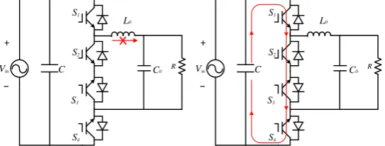
In order to address the voltage fluctuation problems of LVDN, many experts and scholars at home and abroad have done extensive research on the topology and control strategy of dynamic voltage regulator[6]. In numerous researches, AC-AC converters have been extensively studied due to the advantages of simple topology, single-stage power conversion, no DC links, high power factor and so on, so the dynamic voltage regulator based on AC-AC conversion has also got great development [7]. However, the dynamic voltage regulator based on the conventional AC-AC conversion has the disadvantages of unreliable commutation process, short circuit of bridge, dead time and unipolar output voltage [8-9]. The commutation problem of conventional dynamic voltage regulator based on BUCK converter is shown in Figure 1. As shown in Figure 1, in an ideal case, the switches S2 and S3
are both turned ON and OFF simultaneously, and they are complementary to the switches S1and S4
[10]. However, due to the inherent characteristics of the switches itself, there always exists a short dead-time or an overlap-time between switches. During the dead-time, the current flowing in the output filter inductors (L0) has no circulation loop, which may cause the switches to burst. Similarly,
the switches may be damaged by excessive current when there is an overlap-time between switches, because the input voltage will be short-circuited. In order to solve the commutation problem, the usual method is to use lossy of resistor-capacitor (RC) snubbers circuit or to adopt the soft switch commutation strategy. However, these measures can’t reliably achieve commutation when the voltage crosses zero point or the input voltage is distorted [11]. Therefore, traditional dynamic voltage regulators for LVDN containing high proportion of residential PV can’t safely and reliably implement voltage regulation.
In this paper, the bipolar-type dynamic voltage conditioner (B-DVC) based on a novel type of direct AC-AC converter without the commutation problem is proposed. The proposed converters adopt the positive current leg (P-Leg) and the negative current leg (N-Leg) [12]. Because P-Leg and N-Leg structure is adopted, the B-DVC proposed in this paper doesn’t need to set dead-time and can avoid shoot-through problem. In addition, it can operate reliably and robustly even when the voltage or current at the point of common coupling are highly distorted because safe commutation is always guaranteed by the P-Leg and N-Leg structure. The proposed B-DVC can change the polarity of the output voltage by changing the positive and negative duty cycle (D), which can effectively solve the problem of voltage sag or swell. Therefore, it’s possible to solve the current LVDN’s voltage problem with high proportion of renewable energy access. Based on the detailed theoretical analysis, a simulation system is built and an experimental prototype is designed for the proposed topology. Finally, the feasibility and effectiveness of the proposed scheme are verified by simulation and experiments.
C0
L0
R
S1
S2
S3
S4
Vin C
+
-C0
L0
R
S1
S2
S3
S4
Vin C
+
-Figure 1. Commutation of traditional dynamic voltage regulator based on BUCK converter.
Topology Structure of B-DVC based on P-Leg and N-Leg
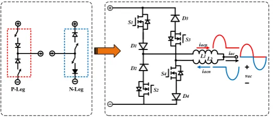
P-Leg and N-Leg
[image:2.595.164.436.541.644.2]indicated by (→) in Figure 2, the current in every P-Leg always flows out from the center terminal, and the current in N-Leg always flows into the center terminal.
The two upper and lower switches in the traditional bridge-leg periodically work alternately. In order to avoid short circuit caused by the two switches short-through, the dead-time must be set during the switching period. However, the separation inductor is placed at the common port of the P-Leg and N-Leg bridge arms, Even if the switching time between P-Leg and N-Leg switches is overlapped, inductor and link stray inductor can limit the rate of current change, so the dead-time is not needed, so the D can be maximized and the conversion efficiency of converter can be improved. At any moment, when the current is in the positive half period, it only flows through the P-Leg; when the current is in the negative half period, it flows through the N-Leg only.
1 D
L1L 2 iacp
iacn iac
vac S1
S3
S2 S4 2 D
4 D 3 D
[image:3.595.164.435.227.343.2]P-Leg N-Leg
Figure 2. Evolution of topology based on P-Leg and N-Leg.
Topology structure of B-DVC
Figure 3 shows the proposed B-DVC topology. Compared with the conventional dynamic voltage regulators, the proposed B-DVC adopts P-Leg and N-Leg structure shown in Figure 2.
AC
Lin
Cin
Lf
Cf
vs
vp
load Power
Grid
S1
S2
S3
S4
S6
S8
S5
S7
Output Input
[image:3.595.144.467.431.625.2]vin
Figure 3. B-DVC of topology based on P-Leg and N-Leg.
Compared with the IGBT, the MOSFET has lower switching loss, resistance characteristics and high frequency. These advantages can ensure the output voltage/current waveform quality and can effectively reduce the size of the filter.
The B-DVC can work in voltage compensation mode or bypass mode. When the grid voltage is normal, the B-DVC operates in the bypass mode adjusting the D of the PWM control signal to zero and the output compensation voltage to zero; when the grid voltage sag or swell, the AC-AC converter generates high-frequency voltage controlled by the D of the PWM signal. After filtering, the sinusoidal AC voltage Vp in the same phase as the grid is obtained. Finally, the Vp is coupled to the distribution network through the power frequency transformer, thereby ensuring the stability of the voltage at the load terminal. When the B-DVC solves the high voltage problem, the polarity of the output voltage is obtained by changing the control strategy, and there is no need to change the voltage polarity through a mechanical switch or a solid state relay. Therefore, compared with the traditional voltage regulator, the B-DVC has the advantages of fast dynamic response, high compensation accuracy, safe and reliable operation.
Operation of the Proposed B-DVC
Switch Signal Modulation
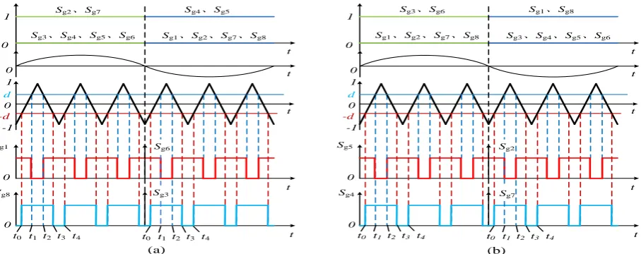
The B-DVC can compensate both voltage sag and swell. A modulation strategy adapted to the topology of Figure 3 is designed according to the different working modes of B-DVC. In this paper, a dual modulation PWM modulation strategy is adopted. In this modulation strategy, the switches S1 S2 S3 and S5, which need to perform high frequency operation, are controlled by modulation signal d(t), while switches S4 S6 S7 and S8 are controlled by modulating signal -d(t). All high-frequency switches take the same triangular carrier signal. According to the different modes of B-DVC, and the positive or negative half-wave of input voltage, the modulation strategy can be divided into Figure 4 and 5. The specific PWM control signal of the corresponding switches is shown in Figure 6.
Sg3
1 d(t) +
0 -1
Sg1
d(t)
Sg8
1 d(t) +
0 -1
d(t)
Sg3
(a) (b)
Sg8
Sg6
Sg3
1 d(t) +
0 -1
Sg5
d(t)
Sg4
1 d(t) + 0 -1
d(t)
(a) (b)
Sg3
Sg5
Sg4
Sg3
Sg2
Sg3
[image:4.595.83.519.462.544.2]Sg7
Figure 4. PWM modulation strategy for voltage sag. Figure 5. PWM modulation strategy for voltage swell.
Sg1
Sg8
Sg2、Sg7
0
0 0 0
0
t
t t
t t
-1 1
d
-d
(a) t0 t1 t2 t3
Sg4、Sg5
Sg3、Sg4、Sg5、Sg6 Sg1、Sg2、Sg7、Sg8
Sg6
Sg3
t4
Sg5
Sg4
Sg3、Sg6
0
0 0
0
t
t
t t
-1 1
d
-d
Sg1、Sg8
Sg1、Sg2、Sg7、Sg8 Sg3、Sg4、Sg5、Sg6
Sg2
Sg7
t0 t1 t2 t3 t4 t0 t1 t2 t3 t4 t0 t1 t2 t3 t4
0 t
1 1
(b)
[image:4.595.73.527.589.769.2]As shown in Figure 4, the PWM modulation strategy for voltage sag, where (a) is the modulation strategy for the positive half period of the input voltage and (b) is the modulation strategy for the negative half period of the input voltage. Figure 5 shows the PWM modulation strategy when the voltage swell, where (a) and (b) is the modulation strategy diagram at the time of the positive and negative half period of the input voltage respectively. In addition, the gate drive signal of Sg1~Sg8 is S1~S8 in Figure 6, which controls the corresponding switches.
Commutation State Analysis of B-DVC
Commutation State of Step-down Mode. When the actual voltage of the Grid is higher than the
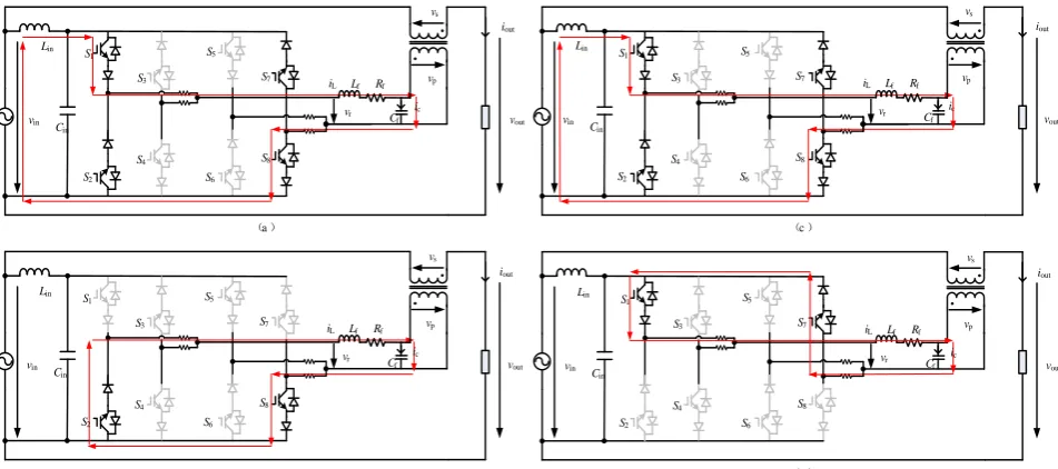
rated voltage, B-DVC works in this mode. Taking the voltage in the positive half-period as an example to analyze the commutation state of the B-DVC. As shown in Figure 7(a), switches S2 and S7 are always in the ON state, switches S3, S4, S5, and S6 are always in the OFF state, and switches S1 and S8 do high frequency actions to achieve a positive half-period energy control of the voltage. The commutation state is divided into four states, as shown in Figure 7 (a) (b) (c) (d). At time t0~t1, as shown in Figure 7(a), the B-DVC operates in an active state. At this point, current flows through S1, inductors, capacitors, S8, and finally back to the power sources. During this time, the power source charges the capacitor. At time t1~t2, as shown in Figure 7(b), the B-DVC operates in a freewheeling state, current flows through S2, inductors, capacitors, and S8, and the capacitor is discharged. Because S2 is always in the ON state, when S1 is turning on to off, the current loop is always exist, and therefore switches are not impacted. At time t2~t3, as shown in Figure 7(c), the operating state of the B-DVC is the same as the time t0~t1, and will not be described again. At time t3~t4, as shown in Figure 7 (d), the B-DVC is in a freewheeling state. At this time, the current flows through S1, inductors, capacitors and S7. When the voltage at a negative half-period, the working state is it is similar to the positive half-period, so it will not be repeated. The specific switches on and off follow the PWM signal shown in Figure 6 (a).
(a)
(b)
(c)
(d)
ic
S1
S3
S2
S8
S5
S7
S6
S4
vin
Lin
Cin
iout
vout
vr C f
ic
Lf Rf
iL
vs
vp
S1
S3
S2
S8
S5
S7
S6
S4
vin
Lin
Cin
iout
vout
vr C f
Lf Rf
iL
vs
vp
S1
S3
S2
S8
S5
S7
S6
S4
vin
Lin
Cin
iout
vout
vr C f
ic
Lf Rf
iL
vs
vp
S1
S3
S2
S8
S5
S7
S6
S4
vin
Lin
Cin
iout
vout
vr C f
ic
Lf Rf
iL
vs
[image:5.595.60.536.440.651.2]vp
Figure 7. Working process diagram of B-DVC with voltage sag and positive half-period.
Commutation State of Step-up Mode. When the actual voltage of the Grid is higher than the rated
charges the capacitors. At time t1~t2, as shown in Figure 8(b), the B-DVC operates in a freewheeling state, the current flows through S4, inductors, capacitors and S6, and the capacitor is discharged. Because the switch S4 is always in the ON state, when the switch S1 is turning on to off, the current loop is always exist and therefore the switches are not impacted. At time t2~t3, as shown in Figure 8(c), the operating state of B-DVC is the same as the time t0~t1, and will not be described again. At time t3~t4, as shown in Figure 8 (d), the B-DVC is in a freewheeling state. At this time, the current flows through S3, inductors, capacitors and S5. When the voltage at a negative half-period, the working state is similar to the positive half-period, so it will not be repeated. The specific switches on and off follow the PWM signal shown in Figure 6 (b).
(a)
(b)
(c)
(d)
S1 S3 S2 S8 S5 S7 S6 S4 vin Lin Cin iout vout
vr C
f
ic
Lf Rf
iL vs vp S1 S3 S2 S8 S5 S7 S6 S4 vin Lin Cin iout vout
vr C
f
ic
Lf Rf
iL vs vp S1 S3 S2 S8 S5 S7 S6 S4 vin Lin Cin iout vout
vr C
f
ic
Lf Rf
iL vs vp S1 S3 S2 S8 S5 S7 S6 S4 vin Lin Cin iout vout
vr C
f
ic
Lf Rf
iL
vs
[image:6.595.73.535.213.409.2]vp
Figure 8. Working process diagram of B-DVC with voltage swell and positive half-period.
Simulation and Experimental Study
Simulation Results
To prove the validity and advantages of the B-DVC proposed, detailed simulation results are presented in this section. Suppose the grid voltage peak is 311V and the load is 10kW pure resistive. The simulation waveform when the voltage sag and swell is shown in Figure 9 and Figure 10, respectively.
Input voltageVin
Compensation voltage Vp
时间/S
Load voltageVout
0. 08 0. 1 0. 12 0. 14 0. 16 0. 18 0. 20 Time/S 400
200
0
-200
-400 voltage/V
Compensation voltage Vp
时间/S
Load voltageVout
0. 08 0. 1 0. 12 0. 14 0. 16 0. 18 0. 20 Time/S 200
0
-200
Voltage/V
Figure 9. Simulation waveform diagram of voltage sag. Figure 10. Simulation waveform diagram of voltage swell.
[image:6.595.67.532.568.698.2]can meet the requirements of voltage fluctuation control in LVDN. Similarly, when the voltage swell of grid occurs, the compensation voltage of B-DVC output is in the same phase and opposite polarity to the grid voltage. It can be seen from Figure 10 that the waveform is slightly distorted when the polarity of the output voltage is reversed, but the duration is very short and doesn’t affect the accuracy of compensation.
Experimental Results
On the basis of the previous analysis, a 10-kW prototype B-DVC is developed and tested, as shown in Figure 13. Table I lists the electrical specifications of the proposed B-DVC. Due to the limitation of laboratory conditions, it’s assumed that the rated voltage amplitude and frequency of LVDN are 155.5V and 50Hz, respectively. When the grid voltage amplitude falls to 100V, that is, when the grid voltage falls 35.7%, the waveform is shown in Figure 14 (a). In addition, when the voltage sag from 20% to a sudden rise of 40%, the waveform is show in Figure 14 (b). From Figure 14 (a) and (b) shows that the B-DVC proposed in this paper can accurately realize the compensation of voltage sags and swells, especially when crossing zero point, there is no commutation problems and voltage isn’t distorted.
Input filter
Output filter
DSP Simulator
DSP
Driver Cooling
[image:7.595.154.442.297.487.2]panel IGBT
Figure 13. B-DVC experimental prototype.
Grid voltage Vin Load voltage Vout Compensation voltage Vp
Load voltage Vout
Compensation voltage Vp
[image:7.595.68.533.511.664.2](a) (b)
Figure 14. Waveform diagram of compensating voltage sag and swell.
Table 1. Parameters of the B-DVC proposed.
Parameter
Input filter inductor
Lin/uH
Input filter capacito
r
Cin/uH
IGBT S1~S8
Switching frequency
/Hz
Output filter inductor
Lf/uH
Output filter capacitance
Cf/uF
Transformer capacity S/MVA
Transformer ratio
Conclusion
In order to address the problem of voltage sag or swell in LVDN with high proportion of residential PV access, a Bipolar-type Dynamic Voltage Conditioner is proposed. The B-DVC adopts a direct AC-AC converter based on P-Leg and N-Leg structure, which overcomes the voltage distortion caused by traditional full-bridge bi-directional switching converter. At the same time, the B-DVC does not need to set dead-time, so the D is maximized, and the efficiency of the B-DVC is improved. In addition, the B-DVC can operate reliably and robustly due to safe commutation is always guaranteed by the P-Leg and N-Leg structure even when the voltage or current at the point of common coupling are highly distorted. Moreover, it can output bipolar voltage without changing the polarity of output voltage by mechanical switches. On the basis of theoretical analysis, the simulation and experimental results show that the B-DVC proposed can quickly adjust the voltage and ensure the stability of the load terminal voltage, which can effectively solve the problem of voltage fluctuation in the LVDN and improve the ability of the LVDN to absorb renewable energy.
Acknowledgement
This research was financially supported by the science and technology project of State Grid Liaoning Electric Power Supply Co. Ltd. (5222SY16000M).
References
[1]El-Naggar A, Erlich I. Control approach of three-phase grid connected PV inverters for voltage unbalance mitigation in low-voltage distribution grids[J]. IET Renewable Power Generation, 2017, 10(10):1577-1586.
[2]Fekete K, Klaic Z, Majdandzic L. Expansion of the residential photovoltaic systems and its harmonic impact on the distribution grid[J]. Renewable Energy, 2012, 43:140-148.
[3]Weckx S, Driesen J. Optimal Local Reactive Power Control by PV Inverters[J]. IEEE Transactions on Sustainable Energy, 2016, 7(4):1624-1633.
[4]Procopiou A T, Ochoa L F. Voltage control in pv-rich LV networks without remote monitoring[C]// IEEE Power & Energy Society General Meeting. IEEE, 2017:1-1.
[5]Long C, Ochoa L. Voltage control of PV-Rich LV networks: OLTC-fitted transformer and capacitor banks[C]// Power and Energy Society General Meeting. IEEE, 2016:1-1.
[6]Babaei E, Kangarlu M F, Sabahi M. Dynamic voltage restorer based on multilevel inverter with adjustable dc-link voltage[J]. IET Power Electronics, 2014, 7(3):576-590.
[7]Barros J D, Silva J F. Multilevel Optimal Predictive Dynamic Voltage Restorer[J]. IEEE Transactions on Industrial Electronics, 2010, 57(8):2747-2760.
[8]Jothibasu S, Mishra M K. A Control Scheme for Storageless DVR Based on Characterization of Voltage Sags[J]. IEEE Transactions on Power Delivery, 2014, 29(5):2261-2269.
[9]Liu H, Wang J. Analysis and control of a single phase AC chopper in series connection with an auto-transformer[C]// International Conference on Automation and Computing. IEEE, 2012:1-6. [10]Shin H H, Cha H, Kim H G, et al. Novel Single-Phase PWM AC–AC Converters Solving Commutation Problem Using Switching Cell Structure and Coupled Inductor[J]. Power Electronics IEEE Transactions on, 2015, 30(4):2137-2147.
[11]Kaniewski J, Szczesniak P, Jarnut M, et al. Hybrid Voltage Sag/Swell Compensators: A Review of Hybrid AC/AC Converters[J]. IEEE Industrial Electronics Magazine, 2015, 9(4):37-48.