Transmission Electron Microscopy and
Spectroscopy of Carbon-based
Nanomaterials
PhD Thesis
Ehsan Rezvani
ASIN Group School of Chemistry
Faculty of Engineering, Mathematics and Science
I, Ehsan Rezvani, declare that this thesis titled, ’Transmission Electron Microscopy and Spectroscopy of Carbon-based Nanomaterials’ and the work presented in it are my own. I confirm that:
This work was done wholly or mainly while in candidature for a research degree at this University.
Where any part of this thesis has previously been submitted for a degree or any other qualification at this University or any other institution, this has been clearly stated.
Where I have consulted the published work of others, this is always clearly at-tributed.
Where I have quoted from the work of others, the source is always given. With the exception of such quotations, this thesis is entirely my own work.
I have acknowledged all main sources of help.
Where the thesis is based on work done by myself jointly with others, I have made clear exactly what was done by others and what I have contributed myself.
Signed:
Date:
Abstract
Faculty of Engineering, Mathematics and Science School of Chemistry
Doctor of Philosophy
Transmission Electron Microscopy and Spectroscopy of Carbon-based Nanomaterials
by Ehsan Rezvani
There are a number of people without whom this thesis might not have been written,and to whom I’m greatly indebted.
I thank my supervisor, Prof. Georg S. Duesberg for his guidance and support.
I would like to thank everyone in the ASIN Group for their support, continual help-ful scientific discussions as well as great humour! Their attitude has made coming to work every day for the last four years a very positive and enjoyable experience, and I have always appreciated the lengths that they have all gone to whenever I needed help. Thanks to Hugo and Niall who have been true friends and invaluable sources of support and advice throughout my study. Thanks to Toby for being a wonderful source of ref-erence and aid endlessly and patiently in all matters. Nina is thanked for her assistance with XPS and her support. Thanks to Shishir a former group member, who generously thought me how to design an experiment properly and showed me the stepping stones of graphene research. Kay and Hye-Young are greatly acknowledged for their constant help and advice on electrical measurements and analysis. Without you,none of those electrical data would have got obtained. Sin´ead and Maria are thanked for their kind support. Thanks to Riley for his technical assistance without whose hands-on skills, isotope graphene experiment would not be feasible. Thanks to Brendan O’Dowd for his generous helps with schematics and and software issues, regularly putting aside his work to help me for as long as was needed. Christian is thanked for being a good friend..
I have greatly enjoyed working at CRANN as well as Advanced Microscopy Lab (AML). In both institutions there is a wealth of experience and advice. I’d like to thank all the staff and researchers here who contribute to the wonderful working environment.
Finally, special and profound thanks to my parents who have been a great source of encouragement and inspiration to me throughout my life. An hour phone conversation with them at a crucial time, helped me find the strength to continue my work here and helped me come to the decision, once and for all, that obtaining this degree would not be the first challenge in my life that I would not rise to meet. And also for the myriad of ways in which always they’ve actively supported me in my determination to find and realise my potential and to make this happen. I’d also like to thank my brothers who offered invaluable support and humour over the years. Words can’t express how much I love you all and how grateful I am for your support. Without you four, I most certainly would not be where I am today.
Declaration of Authorship ii
Abstract iii
Acknowledgements iv
Contents v
Abbreviations ix
1 Introduction and Theoretical Background 1
1.1 Graphene . . . 2
1.1.1 Properties . . . 3
1.1.2 Synthesis of Graphene . . . 4
1.2 Crystal Structure . . . 5
1.3 Growth . . . 8
1.3.1 Theoretical Treatment . . . 8
1.3.2 CVD Process . . . 8
1.3.3 Importance of Layer Number . . . 11
1.4 Electron Microscopy . . . 12
1.4.1 Electron Optics Background . . . 12
1.4.2 Electron-beam Sample Interactions . . . 13
1.4.2.1 Scanning Electron Microscopy . . . 15
1.4.2.2 Transmission Electron Microscopy . . . 16
1.4.3 TEM on Graphene . . . 18
1.4.3.1 Electron Diffraction . . . 20
1.4.3.2 Imaging and Interpretation . . . 23
1.4.3.3 Feature Types on Graphene . . . 24
1.5 Electron Energy Loss Spectroscopy . . . 33
1.5.1 Specimen Thickness . . . 34
1.5.2 Feature Types . . . 34
1.5.3 Graphene Spectrum . . . 37
1.6 Raman Spectroscopy . . . 38
1.6.1 Raman Scattering Theory . . . 38
1.6.2 Raman Spectroscopy of Graphene . . . 40
1.6.2.1 Number of Layers and Stacking Order . . . 41
1.6.2.2 Defects and Disorders . . . 43
1.6.2.3 Effect of Doping . . . 45
1.6.2.4 Effect of Isotopic Composition . . . 45
2 Experimental Methods 47 2.1 Chemical Vapour Deposition . . . 47
2.1.1 CVD Reactors . . . 47
2.1.2 Preparation of CVD Graphene . . . 48
2.1.2.1 Process Steps . . . 48
2.1.2.2 Experimental Set-up . . . 49
2.2 Graphene Transfer to Si/SiO2 wafer . . . 50
2.3 Remote Plasma Functionalisation . . . 51
2.4 Raman Spectroscopy . . . 51
2.5 Scanning Electron Microscopy . . . 53
2.6 Transmission Electron Microscopy . . . 54
2.7 TEM sample preparation . . . 55
2.8 Electron Energy Loss Spectroscopy . . . 57
2.8.1 Spectrometer . . . 57
2.8.2 Energy-Filtered Imaging . . . 58
3 TEM of Carbon-based Nanomaterials 61 3.1 Large-area High-quality Graphene . . . 61
3.2 Graphene as TEM Support . . . 64
3.3 Carbon-Silicon Interfaces . . . 67
3.4 Conclusions . . . 69
4 Modification of CVD of Graphene via Catalyst Optimisation 71 4.1 Suppression of Multilayer Graphene . . . 71
4.2 Methodology . . . 72
4.3 Chromium Influence on Closed Graphene Layers . . . 73
4.4 Time-Resolved Graphene Growth . . . 77
4.5 Isotope Labelling . . . 80
4.6 Proposed Mechanism . . . 82
4.7 Conclusions . . . 83
5 Study of Isotope-enriched CVD Graphene 85 5.1 Isotope-enriched Graphene . . . 85
5.2 Methodology . . . 85
5.3 Isotope-enriched Graphene: Bonding Properties . . . 89
5.3.1 Bond Length . . . 89
5.3.2 Abundant Klein Edges . . . 91
5.3.3 Unusual Heavily Deformed Edge . . . 92
5.4 Conclusions . . . 93
6.2 Remote-Plasma Functionalisation . . . 96
6.3 HRTEM/EELS in Graphitic Materials Research . . . 97
6.3.1 Carbon K-edge EELS features . . . 97
6.3.2 Measurement of Bond Type . . . 98
6.4 Electron Microscopy of Plasma-Treated Graphene . . . 99
6.4.1 HRTEM Studies . . . 99
6.4.2 EELS Studies . . . 101
6.5 Conclusions . . . 102
7 Conclusions and Outlook 103
AC-TEM AberrationCorrected TransmissionElectronMicroscope/y AFM AtomicForce Microscope/y
APS AmmoniumPerSulfate
BF-TEM Bright Field Transmission Electron Microscopy BSE BackScatteredElectron
CBED Convergent Beam Electron Diffraction CCD Charge Coupled Device
CNT Carbon Nano Tube
CVD ChemicalVapour Deposition DFT Density FunctionalTheory
DF-TEM Dark Field TransmissionElectron Microscopy DLC DiamondLikeCarbon
ED Electron Diffraction
EDP Electron Diffraction Pattern EDX EnergyDispersiveX-ray
EELS Electron EnergyLossSpectroscopy
EFTEM EnergyFilteredTransmission Electron Microscopy EKLs ExtendedKLs
ELNES EnergyLossNearEdgeStructure EXELFS EXtended Energy LossFine Structure FFT FastFourierTransform
FWHM FullWidthHalf Maximum GC Glassy Carbon
GFET Graphene Field Effect Transistor GRIP Graphene Resist Interlacing Process
HAADF High AnnularAngleDarkField HOPG Highly OrderedPyrolyticGraphite
HRTEM High ResolutionTransmission Electron Microscopy
HV High Vacuum
IR InfraRed
KIE Kinetic Isotope Effect KLs KLein edges
KLDs KLeinDoublets MFC MassFlow Controller NC NitroCellulose NP Nano Particle
PPF PyrolysedPotoresist Film PyC PyrolyticCarbon
SAED Selected AreaElectronDiffraction SE Secondary Electron
SEM Scanning ElectronMicroscope/y
STEM Scanning Transmission Electron Microscope/y TEM TransmissionElectronMicroscope/y
List of Publications
[1] E. Rezvani, T. Hallam, N. McEvoy, N.C. Berner and G.S. Duesberg. Optimi-sation of copper catalyst by the addition of chromium for the chemical vapour deposition growth of monolayer graphene. Carbon, 95: 789-793, 2015. DOI:
http://dx.doi.org/10.1016/j.carbon.2015.08.114.
[2] E. Rezvani, J.S. Kim,et al.. Aberration-corrected TEM study of isotope graphene.
in preparation, 2015.
[3] J. Conroy, N.K. Verma, R.J. Smith, E. Rezvani, G.S. Duesberg, J.N. Coleman, Y. Volkov. arXiv preprint arXiv:1406.2497, 2014. URL:http://arxiv.org/abs/ 1406.2497.
[4] R. Gatensby, N. McEvoy, K. Lee, T. Hallam, N.C. Berner, E. Rezvani, S. Win-ters, M. O’Brien, G.S. Duesberg. Controlled synthesis of transition metal dichalco-genide thin films for electronic applications. Applied Surface Science, 297: 139-146, 2014. DOI: http://dx.doi.org/10.1016/j.apsusc.2014.01.103.
[5] C. Yim, N. McEvoy, H-Y. Kim, E. Rezvani, G.S. Duesberg. Investigation of the Interfaces in Schottky Diodes Using Equivalent Circuit Models. ACS Applied Materials & Interfaces, 5 (15): 6951-6958, 2013. DOI: http://dx.doi.org/10. 1021/am400963x.
[6] A.K. Nanjundan, H. Nolan, N. McEvoy, E. Rezvani, et al.. Plasma-assisted simultaneous reduction and nitrogen doping of graphene oxide nanosheets. Journal of Materials Chemistry A, 1 (14): 4431-4435, 2013. DOI: http://dx.doi.org/ 10.1039/c3ta10337d.
[7] C. Yim, E. Rezvani, S. Kumar, N. McEvoy, G.S. Duesberg. Investigation of carbon–silicon Schottky barrier diodes. physica status solidi (b), 249 (12): 2553-2557, 2012. DOI:http://dx.doi.org/10.1002/pssb.201200106.
[9] S. Kumar, E. Rezvani, V. Nicolosi, G.S. Duesberg. Graphene resist interlac-ing process for versatile fabrication of free-standinterlac-ing graphene. Nanotechnology, 23 (14): 145302, 2012. DOI: http://dx.doi.org/10.1088/0957-4484/23/14/ 145302.
[10] N. McEvoy, N. Peltekis, S. Kumar, E. Rezvani, H. Nolan, G.P. Keeley, W.J. Blau, G.S. Duesberg. Synthesis and analysis of thin conducting pyrolytic carbon films. Carbon, 50 (3): 1216-1226, 2012. DOI: http://dx.doi.org/10.1016/j. carbon.2011.10.036.
[11] G.P. Keeley, N. McEvoy, H. Nolan, S. Kumar, E. Rezvani, M. Holzinger, S. Cosnier, G.S. Duesberg. Simultaneous electrochemical determination of dopamine and paracetamol based on thin pyrolytic carbon films. Analytical Methods, 4 (7): 2048-2053, 2012. DOI: http://dx.doi.org/10.1039/C2AY25156F.
[12] S. Kumar, N. McEvoy, H-Y. Kim, K. Lee, N. Peltekis,E. Rezvani, H. Nolan, A. Weidlich, R. Daly, G.S. Duesberg. CVD growth and processing of graphene for electronic applications. physica status solidi (b), 248 (11): 2604-2608, 2011. DOI:
Talks
[1] Title: Electron Microscopy and Spectroscopy of Plasma-Functionalised CVD graphene. E-MRS Spring Meeting, Lille, France - 2014
[2] Graphesp2014 Graphene Flagship Meeting, Lanzarote, Spain - 2014
Posters
[1] AMBER Centre Launch, Dublin-2013 (selected as top 8 posters)
[2] Graphene 2013 Conference - Bilbao, Spain
[3] Smart Surfaces, Dublin-2012
[4] Nanoweek Conference, Dublin-2011
Collaborative Posters
[1] Patterned single-layer graphene with metamaterial behavior in the THz range, IRMMW-THz, Arizona - 2014
[2] Detection of critical functional responses to grapheme-based thin films in primary human phagocytes, 14th International Conference on the Science and Application of Nanotubes, Finland - 2013
[3] Multimodal biocompatibility assessment of graphene-based thin films, Nanoweek conference, Dublin - 2012
Introduction and Theoretical
Background
Carbon is able to form strong covalent bonds with itself and other atoms. It can also adopt a number of allotropes, diamond and graphite being two of the most famous ones (see Figure 1.1 (a) & (b)). The discovery of the quasi zero-dimensional C60 molecule (Figure 1.1 (c)) by Curl, Kroto and Smalley in 1985 [1] (for which they were awarded a Nobel Prize) opened a new family of carbon allotropes, known as Fullerenes which includes C60, C70, C82, etc. Following on from this, Iijima reported the discovery of a one-dimensional graphitic carbon structure, now known as a Carbon Nanotubes (CNT) (see Figure1.1(d), in 1991 [2]. The most recent discovery, which brought its discoverers the Nobel Prize in 2010, was a single isolated graphitic layer known as graphene [3] (see Figure 1.1(e)).
Figure 1.1 Schematic representation of various carbon allotropes. (a) Graphite, (b) diamond, (c) fullerene, (d) CNT and (e) graphene (adapted from [4]).
Glassy Carbon (GC), Pyrolytic Carbon (PyC) and so forth. The carbon atoms in these various allotropes can bond in different hybridisation configurations which can be pure
sp, sp2,sp3 or a mixture of them. Diamond has pure sp3 bonds whereas graphite and graphene have puresp2 bonds (with the exception of atoms at the edges of such struc-tures which aresp3-hybridised). Amorphous carbon holds a mixture ofsp2-sp3 bonds, with varying amounts. The ratio between the sp2 and sp3 bonds present in a mate-rial plays an important role in determining its (electrical and mechanical) properties. Therefore it is important to characterise the relative proportions of these bonds [5]. The disordered members of the nanocarbon family are typically produced by means of evap-oration, sputtering, or pyrolysis of carbonaceous materials. For instance, pyrolysis of polymers produces what is known as GC, while Chemical Vapour Deposition (CVD) of hydrocarbons on appropriate materials yields Pyrolytic Carbon (PyC). The crystalline members, namely graphite, fullerenes, CNTs and graphene are typically formed at high temperatures and in the presence of catalysts, where conditions for the growth of larger crystals are met.
1.1
Graphene
1.1.1 Properties
The unique electronic properties of graphene (ballistic charge carriers and high mobility) have inspired a great deal of research and interest in this material. What makes graphene special is mainly its unique electronic properties. Carbon atoms have a total number of six electrons with electron configuration of 1s22s22p2; two in the inner shell and four in the outer shell. In a graphene sheet, there are four orbitals for bonding: three sp2 and one pz. Each carbon atom is bonded to its three closest neighbours via strong in-plane
σ-bonds formed from sp2-hybridised orbitals. The sp2 orbitals yield a trigonal planar structure. The corresponding Bravais lattice to this planar hexagonal structure has two atoms per unit cell. The remaining unhybridised pz orbitals that are extending out of the plane overlap to form π-bonds. The unit cell of graphene contains two π orbitals that disperse to form two π bands (analogous to valence and conduction band). The most important feature of these π bands is that, the gap between them closes at the corners of Brillouin zone, implying the charge carriers in graphene are massless. As a result, the electrons in graphene behave very much like photons and can travel without scattering as fast as approximately 1/300 of speed of light. That is why graphene is an extraordinary conductor of electricity, with an intrinsic charge carrier mobility at room temperature of 200,000 cm2/V.s [9], higher than any other known material.
Figure 1.2 Schematic representation ofσandπbonds in graphene (adapted from [10]).
As well as its electronic properties, the mechanical properties of graphene have also attracted considerable attention. The outstanding mechanical properties of graphene are attributed to the strong network of σ-bonds in a graphene sheet. It has been reported that graphene has a Young’s modulus of 1 TPa and an intrinsic strength of 130 GPa and large spring constant of 1-5 N/m [11–13].
The thermal properties of graphene are equally exceptional. Graphene has an extremely high thermal conductivity up to 5000 W/m.K [14], 20 times higher than that of copper. Moreover, graphene has a large negative thermal expansion coefficient of−6×10⁻⁶ [15], 5-10 times greater than that in graphite.
naked eye when placed on SiO2/Si wafer; and absorbs 2.3 % of the light that passes through it [16]. Due to all these superior properties, graphene has been heralded as a revolutioniser in various research fields and sectors, e.g. energy, electronics, health and costruction. If graphene holds its promise, it can be the material of the century.
1.1.2 Synthesis of Graphene
There are four main approaches to produce graphene: (1) exfoliation (mechanical or chemical), (2) CVD on catalytic transition metal substrates, (3) epitaxial growth on substrates such as silicon carbide and (4) molecular assembly [17] (see Figure1.3).
Mechanical exfoliation is the simplest production method which involves peeling off layers of Highly-Ordered Pyrolytic Graphite (HOPG) one by one, for instance by means of a cello-tape [3]. This method produces the highest quality graphene and therefore is most suitable for lab-scale production where investigation of fundamental physics of graphene is intended. However, this technique has a very low yield and the thickness, size and distribution of the obtained graphene flakes are not controllable; which make this method unsuitable for large-scale production.
Another technique to produce graphene at low cost is by chemical exfoliation. This technique uses a surfactant and sonication energy (or shear mixing) to separate layers of high quality graphite [18, 19]. This method can produce reasonably good quality graphene at commercial scale. Nonetheless, the resulting graphene flakes are typically multilayer and their size does not exceed few hundred micrometres at best. Since this method is a solution-based technique, it is mainly useful for making graphene composites, supercapacitors, printed electronics and chemical applications.
Transfer-free wafer-scale graphene growth is possible by the thermal decomposition of silicon carbide (SiC) [20–22]. Production of epitaxial graphene via this approach involves sublimation of silicon from a SiC substrate at very high temperature to obtain graphene layers. When the SiC is heated in vacuum or in an argon atmosphere, only the silicon atoms leave the surface due to the difference in the vapour pressures of silicon and carbon, and the remaining carbon atoms form epitaxial graphene spontaneously on the surface. This graphene produced by this method is of high quality but it is not really cost-effective due to the extremely high process temperature and the cost of SiC.
Figure 1.3 Diagrammatic comparison of production cost and the associated quality of various production methods of graphene (adapted from [17]).
Finally, the most promising larger-scale graphene growth technique is CVD on a metal substrate. Briefly, a carbon-containing gas such as methane, ethane or propane, decom-poses at high-temperatures and turns into graphene (see section 1.3in this Chapter for detailed description) on the catalytic metal surface [24]. The CVD technique can provide wafer-scale graphene at low cost, which is appropriate for industrial applications. Grow-ing large-area sGrow-ingle crystal graphene without grain boundaries, and removGrow-ing defects and impurities due to the transfer process are the remaining bottlenecks for complete realisation of industrial application [25,26].
Figure 1.3 compares (arbitrarily) graphene production methods and their associated cost and quality. Each of these techniques has its own cost and quality figure of merit and hence will be best suited for particular applications. The production method used throughout the current study was CVD technique. The CVD technique will be discussed in Chapter 2in more details.
1.2
Crystal Structure
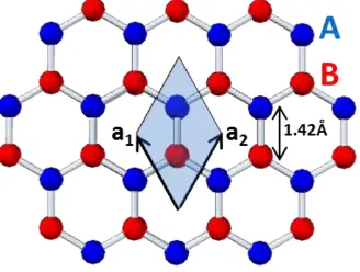
above and below by relatively weak Van der Waals forces. These stacked 2D layers are graphene sheets. The atoms in graphene are laid out flat and each layer is made of hexagonal rings of carbon giving a honeycomb-like appearance. This honeycomb lattice is not a Bravais lattice because two neighbouring sites are inequivalent [27, 28]. Figure 1.4illustrates the graphene’s crystal lattice. A carbon atom located on the A sublattice, has three nearest neighbours in north-east, north-west and south directions; whereas a site on the B sub-lattice has nearest neighbours in north, south-west and south-east directions. The a1 anda2 denote the real space lattice vectors in graphene.
Figure 1.4 Schematic illustration of honeycomb lattice of graphene.
Both A and B sub-lattices however, are triangular Bravais lattices, and one may view the honeycomb lattice as a triangular Bravais lattice with a two-atom basis (A and B). The distance between nearest neighbour carbon atoms is 0.142 nm.
Figure 1.5 Lattice structures of (a) monolayer graphene, (b) AB-stacked bilayer
graphene, (c) ABA-stacked multilayer graphene and (d) ABC-stacked multilayer graphene (adapted from [31]).
In the case of turbostratic graphite, one may distinguish translational disorder from rotational disorder in the stacking which is a crystallographic defect. Generally, the graphene layers in turbostratic graphite are loosely bonded together compared to crys-talline graphite. The simplest case is twisted bilayer graphene, in which the two graphene layers are rotated in relation to one another with an angle ofθ.
1.3
Growth
1.3.1 Theoretical Treatment
Nucleation is a crucial stage during the growth process; therefore, before discussing the case of graphite and graphene growth, a brief theoretical background treatment is presented. The most standard and simple theory that explains the nucleation process is calledclassical nucleation theory. This theory has been successfully applied to describe the graphene nucleation process on the surface of transition metals [36] as well as the growth process of other graphitic thin films [37]. This theory consists of two parts: the thermodynamics part, which deals with the energy evolution upon nucleation, and kinetics that describes the rate at which this nucleation occurs. The thermodynamic part of the classical theory was first developed by J.W. Gibbs in late 19th century, where he first outlined the concept of what is now known asGibbs energy, and how his equation could predict the behaviour of systems. The Gibbs energy is the energy associated with a chemical reaction and the change in the Gibbs energy, ∆G, is used to predict the direction of the reaction at a given pressure and temperature. At constant pressure and temperature, if ∆G is positive, then the reaction is non-spontaneous (i.e., an external energy is necessary for the reaction to occur), and if it is negative, then it is spontaneous (occurs without external energy input).
In most nucleation processes including graphene, there is a substrate on which the reac-tion happens. To account for this, two types of nucleareac-tion processes are discussed within the classical nucleation theory; homogeneous nucleation, that occurs away from a surface and, heterogeneous nucleation which happens on a surface. Heterogeneous nucleation occurs much more often and at a faster rate than the homogeneous nucleation. Hetero-geneous nucleation takes place at preferential sites such as phase boundaries, surfaces or impurities. This is due to the fact that in defect sites/surfaces, a less regular bonding present which leads to a higher energy state, making them reactive. This diminishes the nucleation energy barrier and facilitates nucleation. This holds true for the graphene nucleation on the surface of metal substrates; as has been shown experimentally by various group working on CVD graphene including our own group (see Chapter 5 for empirical examples).
1.3.2 CVD Process
CVD synthesis can be considered the best option to serve this purpose. The preparation of graphite from heterogeneous catalysis on transition metals has been known for years. The first successful CVD synthesis of large-area few-layer graphene was reported in 2008 [38]. Since then, the CVD synthesis has evolved to a scalable and reliable production method of large area graphene. Synthesis of large area and high quality monolayer graphene has been demonstrated by many groups worldwide. The CVD process of graphene on copper was used throughout this work which is elaborated below.
Hydrocarbon-based gas precursors, methane CH4 being the most mentioned, are com-monly used as carbon feedstock for graphene growth. Similar to catalytic graphitisa-tion process, different transigraphitisa-tion metal catalysts are used to reduce the temperature of methane’s decomposition. Among transition metals used for graphene growth, copper and nickel result in high quality graphene and hence, have been most widely studied [39– 41]. Therefore, we can view the graphene growth process, as a heterogeneous catalytic chemical reaction, in which the metal acts as both the substrate and the catalyst itself. This means that, as graphene grows over the metal substrate, it reduces the catalytic activity of the metal as it hinders the catalyst surface exposure to the incoming carbon species. Essentially, if the progress of growth process depends on only surface activated phenomena (e.g. adsorption, decomposition and diffusion of active carbon species), as soon as the catalyst surface is completely blocked (monolayer graphene), the graphene growth process should stop. This is known a “self-limiting” effect and has been observed in copper-catalysed graphene growth, mainly due to the negligible solubility of carbon in copper [24, 39]. On the contrary, for metals that have higher carbon solubility such as nickel, it has been shown that the bulk processes also play a role [38,42].
The overall processes of CH4 decomposition on the copper surface during graphene growth are: (1) active CH4 is broken down into carbon species such as CHx (x=0–3) through dissociative chemisorption on the copper surface, and diffuse on the copper sur-face; (2) once the increasing dynamic concentration of carbon species reaches critical supersaturation level, the nucleation of graphene takes place; (3) part of the supersat-urated carbon species with enough energy reach the graphene domain edge and attach to the graphene domain; (4) the CHx species at the unstable graphene edge detach themselves from graphene, and form dissociative carbon species; (5) Dissociative carbon species combine with hydrogen and are desorbed from the copper surface. Figure 1.6 diagrammatically shows these steps.
Reaction Mechanism
Figure 1.6 Reaction pathways and the active carbon species during CVD growth of graphene on copper from methane as carbon feedstock.
CH4(g) Cu −−* )−− C(s)
Graphene
+ 2 H2(g) (1.1)
However, this overall reaction can be split into more reversible reactions; for instance the following reactions have been proposed to occur [43]:
CH4(g) Cu −−*
)−−C(ads) + 4 H• (1.2)
4 H• −−)Cu−−*2 H2(g) (1.3) C(ads)−−)Cu−−* C(s)
Graphene
(1.4)
As can be seen, H2 appears on the right side of the reversible equation (1.1), which indicates that the partial pressure of H2 in the gas precursor mixture plays a crucial role in the dynamics of the CVD process of graphene. According to Le Chatelier’s principle, reducing the partial pressure of H2 cause the reaction to proceed towards the product or the formation of graphene. Conversely, an increase in the partial pressure of H2 in the reactor will cause the reaction to proceeds to the left or etching of graphene. Furthermore, the dominant form of active carbon species on the copper surface during the growth is also greatly influenced by the partial pressure of H2. Thus, the amount of H2 available extensively affects the growth behaviour of graphene as evidenced in many experiments [44–46]. The detailed investigation of the effect of H2 during CVD of graphene is beyond the scope of this chapter; nonetheless some aspects of this topic are outlined below.
hydrogen, H2. This also leads to the exposure of the pure metal surface to H2 which in turn gives rise to the dissociative chemisorption of H2 on the metal surface. Under typical graphene growth temperature, copper exhibits a significant hydrogen solubility [47,48]. In this case, saturation would be necessary to desorb molecular hydrogen from copper surface. Therefore, before exposure of the catalyst to hydrocarbons, a surface and/or subsurface partially covered with atomic hydrogen could be the starting point [49]. After exposure to hydrocarbons (diluted in molecular hydrogen in most cases), the next step to discuss is the competitive process between the dissociative chemisorption of H2 and the physical adsorption and dehydrogenation of CH4 on available surface sites of the catalyst. During the next steps CH4 catalytic decomposition takes place on the metal surface. The precise moment when the precursor dehydrogenation is completed remains an open question.
It has been shown theoretically that [50], under the conditions of most CVD experiments (including the experimental set-up used in this work), the C• monomer and CH•are two competitive species on the copper, Ir and Rh surfaces. They are more active than CH2• and CH3• and thus the growth of graphene should be mainly due to the attachment of C• monomers and CH• onto the edge of graphene domains. In particular for the copper surface, CH• is a very active carbon species and the combination of two CH• species may induce the formation of C2H2, namely, CH•+ CH•−−→C2H2.
Understanding the CVD growth mechanism and the reaction pathways, is crucial for obtaining high quality large area graphene and ultimately, realisation of commercial products made of CVD-grown graphene [25]. There are still many open questions to be answered in this field, which by itself promises a great potential for future studies.
1.3.3 Importance of Layer Number
parameters of the growth [55, 55,56]. In line with the second strategy, in this work, a novel method for obtaining exclusively monolayer graphene is presented. This is done by modification of the metal catalyst used for CVD growth. The details of this work are presented in outlined in Chapter4. With regards the second strategy, our group has developed a good knowledge and expertise in plasma functionalisation of graphene and related systems. In this thesis, TEM study of such systems is elaborated in Chapter 6.
1.4
Electron Microscopy
Electron optics is the core to most of the works carried out in this thesis. Within this framework, electron beam-specimen interactions form the basis for different characteri-sation techniques described in this Chapter. Thus, in this section, first a brief overview of electron optics and the reason why electrons are used as a “probe” is outlined. Then, various signals produced upon interaction of incident beam with the sample are de-scribed.
1.4.1 Electron Optics Background
Electron microscopy is a characterisation technique that uses a focused beam of energetic electrons produced by an electron microscope, to generate an image from the sample or, to analyse the crystal structure and composition of the sample. The resolution of electron microscope is significantly higher than light microscopes because the electron has a much smaller wavelength than light. Mathematically, the resolution in a perfect optical system can be described by Abbe’s equation:
d= 0.61λ
µsinβ (1.5)
where λ is wavelength of imaging radiation, µ is the refractive index of the medium between source and lens (which is essentially equals 1 in TEM) and β is half aperture angle in radians. The product ofµsinβis often called numerical aperture (NA). Some 50 years after Abbe, on the basis of classical and quantum physics, de Broglie proposed an equation reflecting the wave-particle duality of matter. He proposed that the wavelength of moving particles can be calculated based on their mass and energy levels. The general form of de Broglie formula is as follows:
λ= h
whereh is Planck’s constant,m is mass of the particle and ν is velocity of the particle (the product is momentum p). When an electron is accelerated in TEM through a potential difference, momentum is transferred to it giving it a kinetic energy eV, which should be in turn equal to the potential energy. With an accelerating voltage V, this kinetic energy can be expressed as follows:
eV = 1/2mν2 (1.7)
Now if we restate the equation1.6 and substitute for ν in the equation above, then we will have:
p=mν = (2meV)1/2
(1.8) Replacing this value in de Broglie equation, we can obtain the relationship between electron wavelength and the accelerating voltage of the microscope. In TEM, the electron velocity is close to the speed of light, c, so that the theory of relativity has to be considered therefore theλcan be expressed by the following equation:
λ= h
2meV 1 +2eVmc2
1/2 (1.9)
This formula for electron wavelength can be taken into account in the Abbe’s equa-tion. This means that if we increase the energy of the detecting source (eV term), its wavelength will decrease, and we can get higher resolution [57–59].
1.4.2 Electron-beam Sample Interactions
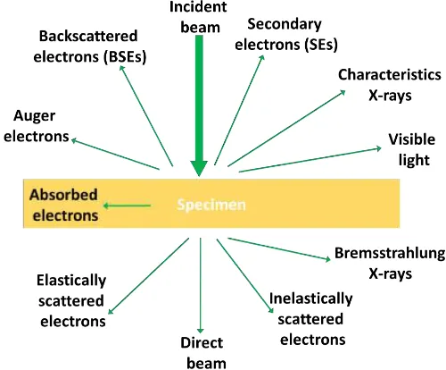
Figure 1.7 Various signals produced upon electron-matter interaction.
the chance of incident electrons to be scattered back out of the sample. By way of analogy, one could imagine the atoms represented as a cluster of snooker balls, and the electron as a smaller ball which is incident on the cluster. From conservation of momentum and the fact the size of an incident electron is fixed, the probability of the smaller ball bouncing backwards is greater the bigger the snooker balls are; which in the case of atoms means higher atomic number. Owing to this specific characteristic, images produced using BSEs show atomic number contrast and, therefore, the features containing higher atomic number elements will appear brighter than those with lower. BSE images are very helpful as they can be used for relatively fast acquisition of high resolution qualitative compositional maps to locate the region of interest in the sample for further quantitative composition analyses.
1.4.2.1 Scanning Electron Microscopy
[image:29.596.173.451.245.440.2]Scanning Electron Microscopy (SEM) is a type of electron microscopy in which a focused beam of electron is scanned over the sample to form an image. When the electron beam hits the sample, both electrons and photons are emitted (heat is also produced). Depending on the depth from which they escape and also their nature, they would carry compositional, topographical and morphological information. Figure 1.8 shows the different signals produced upon electron-matter interaction known as interaction volume.
Figure 1.8 Electron beam-sample interaction volume.
The size and shape of the interaction volume depends mainly on three factors: (1) Atomic number: higher atomic number will result in more interaction of electrons with the atoms of the sample or even stop electrons (lower volume). (2) Accelerating voltage: higher voltages will cause electrons to penetrate further in the specimen which generally results in larger volume. (3) Angle of incidence: greater the angle of incidence, the smaller the interaction volume.
As mentioned above, photons are also generated upon electron-matter interaction and they include characteristic and continuum X-rays. Characteristics X-rays are gen-erated when inner shell electrons interact inelastically with the high energy incident electrons and are excited to outer shell orbitals, creating vacancies in the inner shells. Relaxation of electrons from outer shells to fill these inner shell vacancies, causes X-rays to be produced; which are a function of the elements present in the sample. Not all of the energy created via excitation leaves the sample but some of it is absorbed in-ternally or knocks out an outer shell electron (termed Auger electrons). Characteristic X-rays and Auger electrons carry compositional information where the former technique is more of a bulk technique and the latter is surface sensitive. The technique and/or the instrument to carry out X-ray analysis is termed Energy-Dispersive X-ray Spectroscopy (EDS/EDX). Continuous X-rays or bremsstrahlung on the other hand, are produced when a moving incident charge particle (electrons in SEM) is decelerated by another charged particle which in this case is the electrons of atomic nuclei. The strong electro-magnetic field of nuclei slows the electrons, generating X-ray with an energy equal to the difference in kinetic energy of the electrons before and after the interaction with the nuclei. This property makes these X-rays not useful for characterisation as they are not specific to the material.
1.4.2.2 Transmission Electron Microscopy
TEM is another type of electron microscope which operates on the same basic princi-ples as a light microscope and slide projector. The major difference, of course, is the wavelength of the illumination used: 450–600nm for visible light but only 3.7×10⁻³ nm for electrons accelerated through 100 kV. This difference not only controls the ultimate resolution of the microscope but also its size and shape. This is described later in this section.
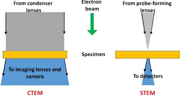
TEM vs. STEM
A TEM can be operated in two modes namely, conventional TEM (CTEM) and scanning TEM (STEM). These two techniques differ primarily in the way they interact with the specimen. The CTEM is a wide-beam technique, which uses a fixed, broad and parallel beam of electrons, that floods the whole area of interest. The image in this technique is formed by an imaging (objective) lens after the thin specimen, and is collected in
Figure 1.9 Schematic comparison between CTEM and STEM.
probe forming lens before the thin specimen. The beam scans across the sample in a raster pattern (see Figure1.9, the scheme on the right). Interactions between the beam electrons and sample atoms generate aserial signal stream. For each probe position (x, y), the signal intensity , I(x, y), and/or spectrum is recorded. Then the image(s) ofI(x, y), or else the integrated signal from the spectral data sets is displayed/recorded [62]. The main advantage of STEM over TEM is that with STEM, there is a better scope for collecting many more signals in a highly spatially-resolved way than we can with TEM. Some of these signals include: secondary electrons, scattered beam electrons, character-istic X-rays, and electron energy loss. Furthermore, we can record different signals in parallel, enabling an improved ultimate resolution and more easily interpretable atomic resolution images. Also, employing a technique called High-angle Annular Dark-field (HAADF) allows recording analytical information at single atom level. This technique is based on detection of electrons that have gone through elastic scattering at high angles. Fortunately, most modern TEM instruments include some sort of STEM capabilities as a standard part.
Lens Aberrations
most. These aberrations are illustrated diagrammatically in Figure1.10. The theory of
Figure 1.10 Schematic illustration of lens defects in a TEM (adapted from [63]).
aberrations in electron optics was proposed only a few years after the invention of TEM by Ruska. Nonetheless, the main barrier ahead of developing correctors, was the lack of engineering knowledge needed to build such correctors. It took some 65 years after the invention of TEM, to realise a spherical aberration corrector with which the resolution of TEM could be improved [64]. About 5 years later, the first commercially available systems for high-resolution TEM came on the market [65]. These advancements have introduced an exciting new area of 21st Century analytical science; which can now allow true imaging and chemical analysis at the scale of single atoms [66]. Up to now, tens of corrected TEM machines have been installed worldwide, and hardware aberration correction has become an almost routinely used technique.
1.4.3 TEM on Graphene
Understanding of graphene has enjoyed an exponential increase since its discovery and electron microscopy has been a key element in this phenomenon. But the advances in the physics of graphene that have been achieved by electron microscopic studies, should be set in the broader context of electron microscopic studies ofsp2 bonded nanocarbons as a special class of materials.
new form of carbon C60 had a closed cage structure and it constituent atoms were con-veniently, all of the same mass, making it particularly suitable for mass spectroscopy [1]. Since CNTs may possess a variety of lengths and diameters, mass spectroscopy was not suitable to confirming their presence. It was HRTEM however, that could first confirm CNTs and provide clear image evidence of their existence [2].
It was however, the experimental isolation of graphene [3], and subsequently, the prepa-ration of free-standing graphene membranes [6,67], that paved the way to a whole range of new possibilities to study thesp2 bonded carbon in the most direct way. Beneficially, the projected image of a monolayer membrane can be easily interpreted in terms of individual atomic positions (rather than atomic columns), allowing study of the fun-damental properties of sp2 bonded carbon atoms. Hence, the graphene membrane and investigation of its quality, are of particular interest for the science and applications of this promising new material. The power of direct images becomes more apparent in revealing the atomic configurations of lattice imperfections, such as point defects, grain boundaries, functional groups or edges. Sub-nanometre imaging of this sort has only become possible in recent years, and is still beset with a range of difficulties includ-ing preparation of clean large-area TEM samples. Prior to availability of low-voltage HRTEM, structural characterisation of graphene was primarily carried out using Raman, Atomic Force Microscopy (AFM) and optical microscopy (typically graphene was trans-ferred onto SiO2/Si wafers for these analyses [68–71]). However, in order to investigate graphene’s atomic structure, HRTEM is invaluable.
The optics of TEM can be used to make images of the electron intensity emerging from the sample. For example, variations in the intensity of electron diffraction across a thin specimen, calleddiffraction contrast, is useful for making images of defects such as dislo-cations, interfaces, and second phase particles. Beyond diffraction contrast microscopy, which measures the intensity of diffracted waves, is HRTEM in which the phase of the diffracted electron wave is preserved and interferes constructively or destructively with the phase of the transmitted wave. This technique ofphase-contrast imaging is used to form images of columns of atoms.
1.4.3.1 Electron Diffraction
Diffraction is an interference effect which leads to the scattering of high energy beams of radiation in specific directions. Diffraction from crystals is described by the Bragg’s Law:
nλ= 2dsinθ (1.10)
wheren is an integer (the order of scattering),λis the wavelength of the radiation,d is the spacing between the scattering entities (e.g. planes of atoms in the crystal) andθis the angle of scattering.
When a beam of high energy electrons is used as the radiation source, the technique is called Electron Diffractometry (ED) and the resulting regular array of bright spots created by this interaction is termedElectron Diffraction Pattern (EDP). ED refers to a collective scattering phenomenon with electrons being (nearly elastically) scattered by periodic arrays of atoms as found in a crystal. The incoming plane electron wave interacts with the atoms, generating secondary waves which interfere with each other. This occurs either constructively (reinforcement at certain scattering angles generating diffracted beams), or destructively (vanishing of beams). Similar to X-Ray Diffraction (XRD), these scattering events at crystal lattice planes can be described by equation 1.10. In this interaction, the atoms of the crystal act as a filter for the incident electrons,
causing them to scatter in certain angles predicted by Bragg’s Law. Each set of parallel lattice planes, generates a pair of spots in the EDP with the direct beam in their center. Since the wavelength λ of the electrons is known, interplanar distances can then be calculated from EDPs. Moreover, it is possible to deduce the symmetry of the crystal using ED-based analysis. These potential applications, make electron crystallography a powerful technique for “solving” crystal structures, both in physical and life sciences [72,73].
from the area selected in the image mode. SAED can be performed on the regions in the order of <0.5µm diameter, but spherical aberration of the objective lens limits the technique to regions not much smaller than this. Providentially, it is possible to focus the electron beam to a small diameter and perform ED work at nanometre range. This method is termed Convergent Beam Electron Diffraction (CBED). (c) Since ED studies are typically performed in a TEM, the imaging capability of the microscope can be employed while the EDP is recorded. This is particularly important in the field of low-dimensional materials science when only very small features within a sample are of interest. One can calculate the interplanar spacing in the crystal being studied using the separation of spots in the DP. For this purpose, we need to first revisit the Bragg’s equation. Since the ED angles are very small (0◦ <θ <2◦), therefore we have:
sin(θ)≈tan(θ)≈ 1
2tan(2θ) (1.11)
We can depict the geometry of electron diffraction as shown in Figure 1.11:
Figure 1.11 Schematic illustration of geometry of electron diffraction and the concept of camera length L.
From the geometry of Figure 1.11we can write:
tan(2θ) = r
L (1.12)
which we can then substitute this into equations (1.10) and (1.11) to obtain:
rd=λL (1.13)
wherer is the distance from the central spot, d is interplanar spacing and the product
λLis calledcamera constant, whose unit is usually ˚A.cm and can be found in the manual of any TEM instrument.
Electron Diffraction Study of Graphene
as graphene, how diffraction could occur? For any diffraction condition the Bragg’s law should be satisfied which contains the parameter d, the inter-planar spacing, whereas graphene is only one layer. The answer lies in the fact that in case of a 2D crystal, the reciprocal lattice is formed by rods (see Figure1.12 (a)) instead of discrete points as in case of a 3D crystal. In other words, the condition that the scattering wavevector has to intersect the reciprocal lattice, only applies to the components parallel to the lattice which means in the graphene plane in our case.
Figure 1.12 Schematic representation of reciprocal space of (a) Monolayer and (b) Multilayer graphene.
As can be seen in Figure1.12(b), the rods are discontinuous due to the additional layers on top of perfect 2D monolayer graphene. To label equivalent Bragg reflections, Miller-Bravais indices [hkil] for graphite is used so that the innermost hexagon of diffraction spots corresponds to [1¯100] and the next one to [11¯20] indices. Figure 1.13 depicts the above-mentioned directions and planes in the graphite lattice.
Figure 1.13 Crystal directions analysed in diffraction pattern study of graphene and graphene layers.
is nearly equal to one (see Figure 1.14 (a) & (c)). For an AB-stacked bilayer sample, Figure 1.14 (b) & (d), the [11¯20] intensity is ≈ 4× higher than the [1¯100] intensity. in general, for crystalline Bernal- or ABC-stacked multilayer samples the [11¯20] intensity is stronger than the [1¯100] intensity.
Figure 1.14(a) EDP of a monolayer graphene membrane, and (b) a bilayer membrane. A profile plot along the line between the arrows is shown in (c,d) (adapted from [75]).(e) TEM image of a CVD graphene suspended on a TEM grid. The inset is the corresponding DP. (f) The intensity profile along the red line in DP.
The EDPs can also provide a first indication of defect density. The mean deviation from a regular lattice, reduces the intensities of the higher order reflections [76]. Therefore, potentially a highly- defective few-layer graphene sheet, where the [11¯20] intensity would be reduced, might be mistakenly identified as a monolayer. Furthermore, as mentioned above, an AA stacked multilayer graphene would produce the same pattern as monolayer graphene (however, reports of AA-stacked graphite are quite rare). For an unambiguous identification of monolayer graphene from electron diffraction data, one needs to obtain a series of diffraction patterns with the sample tilted to different orientations; or use other supplementary techniques such as Raman spectroscopy.
1.4.3.2 Imaging and Interpretation
go through it. If the direct beam is selected, the resulting image is called a bright-field (BF) image (Figure 1.15 (b)); and if the scattered electrons of any form is selected, it is called a dark-field (DF) image (Figure 1.15 (b)). For each imaging mode shown in Figure 1.15, an actual TEM image is depicted at the bottom of the diagram, for further clarity. The most notable difference between these two mode is that the image contrast is inverted in relation to one another. This is due to the mechanism of image formation in each case. Since BF images are formed by weakening of direct beam upon interaction with the sample, a mass-thickness contrast is in effect. Thus, the areas in the sample that contain heavier elements, appear darker. Whereas for an DF image, the diffracted beams are the main contributor to the image formation; thus DF images contain information about the crystal lattice such as imperfections and a more reliable composition contrast comparing to the BF image.
Figure 1.15Schematic illustration of (a) Bright Field (BF) imaging mode. (b) Dark Field (DF) imaging mode. The diagram is adapted from [74], images are owned.
1.4.3.3 Feature Types on Graphene
atomic thickness negates many of the conventional sample preparation issues, and thus is a perfect specimen for study by low-voltage AC-TEM, allowing the probing of atomic scale defects in the graphene structure at high spatial and temporal resolution. Below, some of the most important TEM feature types of graphene are presented.
Graphene lattice at atomic resolution
HRTEM images are formed by interference of diffracted and transmitted electron beam with the sample and the modulation of the phase of electron wavefunction after the sample. Thus, HRTEM images are inherently more difficult to interpret compared to the traditional optical and electron microscopy techniques where the change in the amplitude of the incident beam wavefunction is used for image formation. Therefore, the HRTEM image obtained on the detector is not necessarily a direct image of the atomic positions [57].
Figure 1.16 HRTEM images of graphene honeycomb lattice. (a) Image taken by a non-AC TEM machine. (b) Image recorded in a AC-TEM machine. The overlaid hexagons are guides to the eye. The scale bars are 0.5 nm.
There are two factors that should be taken into account when HRTEM analysis is performed, the modification of the incoming electron wave by the sample, and a further modification of the exit wave after the sample by the electron optics of the microscope. Fortunately, the effect of the sample can be considered negligible for one-atom thick, light-element samples such as graphene. A consequence of this approximation is that, we can simply interpret regions of dark contrast as regions of high electron density, making image interpretation markedly more straightforward.
Hence, correcting for the lens aberrations is essential when precise HRTEM analysis of atomic positions is intended. This is the basis of the work presented in Chapter 6. Perhaps the most familiar and simplest TEM feature of graphene is HRTEM image of honeycomb lattice of graphene. Figure 1.16shows a non AC-TEM image together with a HRTEM taken by AC-TEM for the comparison. While one can clearly distinguish the hexagonal network of graphene lattice in the right-hand side image, the one at the left only contains a hint of graphene lattice.
Defects in Graphene
In a defect-free graphene lattice, each carbon atom is bonded to three neighbouring carbon atoms, with identical 120◦ in-plane bonding angles. The presence of structural defects breaks this perfect symmetry and opens a whole research area for studying the effect of structural defects on the mechanical, electrical, chemical, and optical properties of graphene. Nonetheless, sometimes their effect is beneficial. For instance, defects are essential in chemical and electrochemical studies, where they create preferential bonding sites for attachment of desired functionalities [78, 79]. On the other hand, defects pose a problem for electronics applications such as field-effect transistors because they can significantly lower the charge carrier mobility and thus increase the resistivity of graphene sheet [80, 81]. Given their crucial impact on graphene properties, it is important to control defect formation and, if possible, find ways to repair existing defects. The superior resolving power of modern AC-TEM systems permits the imaging of atomic defects in the graphene lattice.
As a two-dimensional crystal, one can identify three main types of defects in the graphene lattice: point defects (e.g. vacancies and Stone-Wales (SW) rotation, adatoms, substi-tutions and interstitials), line defects (e.g. dislocations and grain boundaries) and edge imperfections. In the second type of defect, one carbon atom is replaced by another atom of a different element or, an adatom is incorporated into the lattice without replacing any carbon atom. Below, these defects are discussed except for line defects. However, grain boundaries in graphene is discussed as one of the most important TEM studies of graphene.
Point Defects
Stone-Wales Defect
5-and two 7-membered rings, as illustrated in Figure1.17(a, b) [82]. This defects requires 9-10 eV energy to be created which means further creation of such defects is very unlikely at room temperature (T=298 K therefore kT=0.0257 ev). However, under the effect of electron beam irradiation inside the TEM, this energy can be supplied. For instance, at 80 kV TEM analysis, a kinetic energy of ≈80 eV is imparted to the specimen which is sufficient to create a SW rotation.
Figure 1.17 Schematic model of Stone-Wales defect (adapted from [83]).
Vacancies
In a vacancy defect, one or more atoms are removed from the lattice and the resulting perturbation to the lattice is relaxed by one or more SW rotations. Vacancy defects in graphene are not easily formed. The energy required to sputter a single atom out of the lattice is in the range of 10-22 eV [84], depending on the type of vacancy. Such energy can not be achieved unless the lattice is irradiated with high energy ions or by electrons in a TEM environment (>80 kV for graphene). These kinds of defects act as strong scattering centres for the charge carriers in graphene [85]. Vacancies can also act as occupancy sites for substitutional impurities, and can also exhibit complex structures when combined with multiple SW bond rotations defects.
Monovacancy
The ejection of a single carbon from the graphene lattice yields a monovacancy (see Figure 1.18 (a)), which leaves the graphene lattice with three under-coordinated edge carbon atoms (Figure 1.18 (b)), each of which possesses a single dangling bond. To minimise the energy the defect can undergo a geometric distortion, with a bond recon-struction between two of the under-coordinated carbon atoms, resulting in a 5-membered and a 9-membered ring (Figure1.18(c)). This structure is rather unstable as it contains under-coordinated carbon atoms. Thus, its observation in TEM is infrequent [84].
Divacancy
Figure 1.18 Schematic model of monovacancy point defect (reproduced from [86]).
electron exposure as all the carbon atoms involved are sp2 bonded [87, 88]. The most
Figure 1.19 (a) Smoothed AC-TEM image of a reconstructed divacancy in graphene. (b) The annotated version of the (a). The numbers denote the the number of carbon atoms in the ring. Scale bar is 0.25 nm.
basic transient configuration is 5-8-8 ring patter. This structure is fairly unstable and under the effect of electron beam in TEM, can transform to other ring patterns [87,88]. For instance, structures such as 555-777, 5555-6-7777 have been reported (the numbers denote the carbon count in a ring) [84]. Other ring patterns may also form by a SW rotation of a bond in the produced structure. Figure 1.19 shows an example of such reconstructed divacancy in graphene lattice.
Multivacancies
Higher number of vacancies are also probable in the graphene lattice to be formed. However, they require highly-focused beam bombardment and/or prolonged exposure to the beam. Figure 1.20 shows a schematic model of possible multivacancies in graphene lattice.
Figure 1.20 (a–d) The relaxed atomic models of multivacancies in graphene (double, tetra, hexa and dodeca, respectively). ‘P’ indicates the five-atom rings and Vndenotes the number of vacancies (adapted from [89]).
Introduction of dopants and foreign atoms into the graphene lattice is necessary for many applications such as functionalisation, sensing and bandgap engineering. Adatoms typically occupy one of three high symmetry sites on the graphene lattice known as bridge (B), hollow (H) and top (T) sites [90]. These sites are shown schematically in Figure 1.21. Figure 1.21 (b) shows a filtered AC-TEM image of a graphene edge, containing many larger foreign atoms (marked by yellow dashed circles and arrows). Given the size of these atoms, it is postulated that they have incorporated in H positions. However, precise assignment of the incorporation site, requires further localised compositional data.
Figure 1.21 Adatoms in graphene. (a) Depending on the element, adatoms favour either the high-symmetry bridge (B), hollow (H), or top (T) position in the graphene sheet (adapted from [91]). (b) Filtered AC-TEM image of a graphene edge, containing a number of large foreign atoms. Scale bar is 0.5 nm.
Edges
[image:44.596.93.469.244.687.2]A great deal of interest has been vested in the study of graphene edges, in particular their effect on graphene nanoribbons; structures that exhibit modified electronic properties to that of bulk graphene [92, 93]. The edges of graphene can terminate in four main ways, namely zigzag, armchair, reconstructed edges and Klein edges and their variations [94, 95]. Figure 1.22 shows smoothed and inverted AC-TEM images of the zigzag, armchair, reconstructed zigzag structure and Klein edges and corresponding annotated images for more clarity. The armchair and zigzag configurations result from terminating
graphene along the lattice line without any reconstruction [92]. AC-TEM imaging and supporting calculations [96,97], have demonstrated that the formation of a reconstructed zigzag state is of lower energy than the metastable zigzag configuration. It is possible to capture the formation of dangling, single bonded carbon atoms projecting from the graphene zigzag edge; these are known as Klein edges [98] and two of them are show in Figure 1.22 (d) (white arrows). The relative stability of these edges, as well as various observed Klein edges, are elaborated in Chapter 5.
Identifying the number of layers
As mentioned previously in this Chapter, There are several non-destructive techniques for determining the layer count of a graphene sample, some of which do not require the high resolution of an AC-TEM and yet sensitive enough (e.g. Raman spectroscopy). Nonetheless, by employing focussed electron beam sputtering of the graphene sheet at
Figure 1.23Identification of layer count in a bilayer graphene sheet. The numbers denote the layers count in different parts of the image. The white spot encircled with dashed white is a debris on CCD camera of the microscope.
a high current density (80 kV) it is possible to open up holes in the graphene sheet. Figure 1.23shows a bilayer graphene example, with the region irradiated until vacuum was visible. The number of layers are colour coded for more clarity.
Ripples in Graphene
First and foremost, the presence of ripples in graphene sheets which accounts for the stability of two-dimensional graphene, was first confirmed via electron diffraction (ED) studies carried out using TEM [99]. This complementary technique, is generally the most accurate approach for studying ordered (crystalline) configurations and, to some extent, the spatially averaged deviations from the regular lattice. The clue that led to the realisation of ripples of suspended graphene was broadening of the diffraction spots, caused by tilting of surface normals, caused by tendency of carbon atoms to form the more stablesp3 structure (see Figure 1.24).
Figure 1.24 The corrugation of suspended graphene sheets. (b) The variation in surface normals leads to non-zero intensities on cones instead of rods in reciprocal space. (c) As a result, ED patterns obtained with a tilted sample (here15◦ with horizontal tilt axis) show a broadening of the diffraction spots (adapted from [6]).
Grain Boundaries
The next example is observation of the grain boundaries in CVD-grown graphene using TEM. The CVD synthesis of graphene on transition metal surfaces (e.g. nickel and copper), yields large-area graphene sheets. Nevertheless, the graphene sheets produced by this method are polycrystalline with grain boundaries between domains of different orientation [24, 38, 42]. Grain boundaries in general, had been predicted to contain non-hexagonal configurations as a periodic array of dislocations [100,101] although the precise arrangement was not clear. The resulting grain boundaries between monolayer graphene areas were imaged for the first time by Huanget al. [102] and Kimet al. [103]. Figure1.25shows an annular dark field (ADF)-STEM image (atoms appear white) of a grain boundary in a large-area polycrystalline graphene sheet synthesized on copper and subsequently transferred to a microstructured TEM grid [102]. In Figure 1.25 (c)–(d), one can clearly see the grain boundary structure: carbon pentagons and heptagons are found at the grain boundary, oriented in such a way that all carbon atoms are in a
configurations on a nanometre scale and the latter is sensitive to crystal orientations on a micrometre scale.
Figure 1.25 Annular dark field STEM images of graphene and grain boundaries in graphene (a) low-magnification image of CVD graphene membranes on a support grid. (b) High-resolution image of the graphene lattice. (c) Image of a representative grain boundary, and (d) the same image with pentagons, heptagons, and a few hexagons outlined. Scale bars are (a)5µm, (b)–(d)5 ˚A (adapted from [102]).
1.5
Electron Energy Loss Spectroscopy
As previously mentioned, in TEM, incident electrons interact with the specimen atoms in three possible ways: elastic scattering, transmission through the specimen or inelastic scattering. Upon the first two types of interactions, the energy of incident electrons remains more or less unchanged; whereas in the latter case, the electrons lose some of their energy during this interaction. The energy loss of such electrons is directly related to the specimen atoms and the electron shells from which the inelastic scattering has occurred. The amount of the energy loss can be measured by means of a spectrometer, located in or after the TEM column, and be displayed as a plot. This plot shows a count of how many electrons have lost what extent of energy and is termed Electron Energy Loss Spectrum (EELS); the y-axis in an EEL spectrum corresponds to the number of electrons or count and the x-axis represents the energy loss. The probability of the scattering events is proportional to
√
Z
V ; where Z is the atomic number and V is
accelerating voltage of the incident electron beam and λe
λi ∼ 10
Z ; where λe and λi are
1.5.1 Specimen Thickness
There are many types of inelastic processes including single scattering and plural scatter-ing. The specimen thickness, which is of great importance in analytical TEM, influences the probability of these scattering events. These two types of scattering are shown schematically in Figure 1.26.
Figure 1.26 Schematic illustration of single and plural scattering and the mean free path of inelastic scattering equation.
The plural scattering is detrimental to the edge visibility as it increases the background noise. The probability for n times scattering is described mathematically by Poisson distribution:
Pn= (
t λi
)n.exp(−t
λi
)/n! (1.14)
Where t is specimen thickness. In order to get reliable results from EELS, the sample thickness should be less than mean free path value which is normally satisfied by a maximum 50 nm-thick sample.
1.5.2 Feature Types
Three main regions can be identified in a typical EEL spectrum: zero-loss, low-loss region and high-loss region (see Figure1.27) ; Each of these features has its own origin and carries specific information. The characteristics and relevant analytical applications of each of these regions are outlined below.
Figure 1.27 A typical EEL spectrum (adapted from [104]).
decreases. The ZLP is not that informative and may even cause damage to the CCD camera if enough care is not taken during acquisition of the spectrum simply because it is very intense.
Low-Loss Region. This regions normally expands to about 50 eV energy loss and originates from the interaction of the beam with the weakly-bound outer shell electrons in the sample. This interaction causes longitudinal wavelike oscillations of (quasi)free electrons in the valence or conduction band and generates a characteristic loss termed Plasmon Loss. Energy loss due to plasmon excitation (EP) depends on the local density of free electrons (n) which is affected by the sample chemistry; therefore plasmons can be used for microanalysis. The lifetime of plasmons is too short (about 10−15s) and they decay either in the form of photons or phonons. Plasmons are localised to<10 nm, carry contrast information and can limit image resolution by chromatic aberration. The low-loss part of spectrum can also be used to accurately measure the relative thickness (t/λ) of the thin films:
t=λln(Itot
I0
) (1.15)
measurements using monochromated electron source [106–108], chemical analysis and probing the optical properties [109].
High-Loss Region. This region includes energy losses >50 eV and originates from interaction of electron beam with inner shell electrons leading to excitation to an unoc-cupied orbital above the Fermi level. This ionisation loss process results in generation of characteristic elemental energy loss edges (e.g. K, L and M) which is unique for each and every element. Typically the K-edge has a sharp onset whereas in other edges while the sub-shell transitions can be resolved individually, the energy dispersion of the edges are broader. These are high energy processes and there is a minimum threshold value,
EC, that must be transferred from the incident electron to the inner-shell electrons for
them to be able to escape from their orbitals (this energy is the binding energy of the inner-shell electron to the nucleus of atom). At the same time, however, ionisation also occurs with larger energy losses E>EC. The ionisation edge intensity is smaller than
those of plasmons; and the closer a primary electron gets to the nucleus of an atom, the larger the energy loss becomes.
Energy-Loss Near Edge Structure (ELNES)
Features whose energy loss lie between EC <E <EC+50 eV are called Energy Loss Near Edge Structures (ELNES) and essentially reflect the density of unoccupied states [110]. Some of the applications of ELNES are as follows: (a) Identification of transition metals. If the d shell is empty, L2 and L3 will split. By measuring the ratio of the L edges, the type of the transition metal can be identified. (b) Orientation. In anisotropic crystals, ELNES changes with the alignment of the momentum transfer along different crystallographic directions. (c) Chemical shifts. This effect is due to charge transfer in the valence band which eventually leads to a shift in the edge threshold. An example is distinguishing different oxidation states of titanium from the appearance of edges. (d) Fingerprinting information for differentiating specific phases. An example of the carbon K-edge ELNES of a number of carbon-based compounds and some carbon allotropes are shown in Figure 1.28. In this example, one can see the clear evolution of π* an
Figure 1.28 Carbon K-edge ELNES of different C-related compounds highlighting the fingerprinting ability of ELNES technique (adapted from [111]).
1.5.3 Graphene Spectrum
Figure 1.29 (a) Low-loss spectra of single-, double-, and five-layer suspended graphene, recorded using 100 keV electrons [112]. (b) Carbon K-edge recorded using 200-keV electrons from single-layer free-standing graphene. The K-edge of a double layer appeared similar [113].
1.6
Raman Spectroscopy
1.6.1 Raman Scattering Theory
Figure 1.30 Energy diagram of elastic and inelastic scatterings. The thickness of the arrows represents the intensity of each type of scattering.
phonon excitation) is called Stokes shift. However, if the opposite process happens and the scattered photon gains energy during the process, this energy difference is termed
Anti-Stokes shift; in other words the scattered photon shifts to a higher frequency than the incident light. This additional energy comes from dissipation of thermal phonons in the crystal, cooling it down during the process. If we express the energy and momentum of the incident photon withEL and kL respectively, those of scattered photon withESc
andkSc, andEqandq for those of phonons, then for energy and momentum conservation
we must have:
ESc=EL±Eq and kSc=kL±q (1.16) In the Stokes process, a phonon is created thus the (+) sign in the equations 1.16, whereas in anti-Stokes a phonon is annihilated so the (-) sign. The ±Eqare in fact the Raman peaks that appear in the spectrum. Conventionally, the positive energies are assigned to Stokes shifts and negative energies to anti-Stokes. Given the spectrometer divides the scattered light into two different directions, the anti-Stokes signal appears in the opposite position in relation to the Stokes signal. The probability of these processes depends upon the excitation energyEi and the temperature.
![Figure 1.3 Diagrammatic comparison of production cost and the associated quality ofvarious production methods of graphene (adapted from [17]).](https://thumb-us.123doks.com/thumbv2/123dok_us/0.918518/19.596.172.463.85.343/figure-diagrammatic-comparison-production-associated-ofvarious-production-graphene.webp)
![Figure 1.5 Lattice structures of (a) monolayer graphene, (b) AB-stacked bilayergraphene, (c) ABA-stacked multilayer graphene and (d) ABC-stacked multilayer graphene(adapted from [31]).](https://thumb-us.123doks.com/thumbv2/123dok_us/0.918518/21.596.110.524.74.300/lattice-structures-monolayer-graphene-bilayergraphene-multilayer-multilayer-graphene.webp)

![Figure 1.10 Schematic illustration of lens defects in a TEM (adapted from [63]).](https://thumb-us.123doks.com/thumbv2/123dok_us/0.918518/32.596.174.380.107.342/figure-schematic-illustration-lens-defects-tem-adapted.webp)

![Figure 1.14 (b) & (d), the [11¯20] intensity is ≈ 4× higher than the [1¯100] intensity](https://thumb-us.123doks.com/thumbv2/123dok_us/0.918518/37.596.109.524.160.371/figure-b-d-intensity-higher-intensity.webp)

