Development of an Audio Transmission System
Through an Indoor Visible Light Communication
Link
Jawad Tahmeed Bin Taufik*, Mohammad Liton Hossain**, Tafiq Ahmed ***
* Electrical Engineering, University of Rostock, Germany
**Department of ECE, Institute of Science and Technology, National University ***Electrical Engineering, University of Rostock, Germany
DOI: 10.29322/IJSRP.9.01.2019.p8556 http://dx.doi.org/10.29322/IJSRP.9.01.2019.p8556
Abstract- This study presents an approach to develop an indoor visible light communication system capable of transmitting audio signal over light beam within a short distance. Visible Light Communication (VLC) is a pretty new technology which used light sources to transmit data for communication. In any communication system, both analog and digital signal transmission are possible, though, due to having the capability of providing a faithful quality of signal regeneration after the transmission process, digital communication system is much more popular than the analog one. In the current project, digital communication process was adopted also. To convert the analog audio signal into the digital transmission signal and vice versa, Pulse Width Modulation (PWM) was used as the signal encoding strategy. As the light emitter, white Light Emitting Diodes (LEDs) were used and as photo sensor, a solar cell was used instead of a photodiode to obtain greater signal power and sensitivity. In the system, the carrier signal for transmission was chosen to have a frequency of 50 KHz. At the receiving end, a 4th order Butterworth lowpass filter having a cutoff frequency of 8 KHz was used to demodulate the audio signal. Using only 2 white LEDs, the indoor transmission range of this visible light communication system was found to be 5 meters while reproducing a satisfactory quality audio.
Index Terms- Visible Light Communication System; Analog; Digital; Pulse Width Modulation; Solar Cell; Photodiode; Carrier Signal; Butterworth low pass Filter; Cuttoff Frequency.
I. INTRODUCTION
Visible light communication (VLC) is a wireless data communication system which uses the visible light spectrum between 400 and 800 THz (780–375 nm) as the data carrying medium. Visible light spectrum is a part of the total electromagnetic spectrum, which is visible to human eyes and harmless like other high frequency electromagnetic waves. Basically, any visible light communication system transmitter modulates light from a light source with the desired data and throws it onto a distant receiver whereas, in the receiver, this
[image:1.612.327.576.349.461.2]modulated data is decoded again to reconstruct the desired signal. Applications of VLC in our day to day life include transmitting various kinds of data along with room lighting system, HD video streaming, access to internet, making computer LANs, wireless printing, wireless surround sound speaker system etc. Pairing and communicating with high speed digital data between two or more digital devices via light is known as Li-Fi [1].
Figure 1. The Electromagnetic Spectrum.
Most of the modern wireless communication systems nowadays use very high frequency electromagnetic waves (usually between 300 MHz and 300 GHz) which is also called ‘Microwave’ and these high frequency waves can cause serious health hazards for humans and other living being [2].
With the increasing number of users, the wireless communication provider companies are setting up more high power transmitter towers in localities. High frequency microwave radiations are thought to be a primary cause of different types of cancers. On the other hand, light, which is also electromagnetic wave, is not harmful for living being though its frequency range is much higher than microwaves. Also, being higher frequency wave, light can potentially carry more data having a higher bandwidth. Moreover, being safe for human being, visible light communication could be the next generation worldwide communication system.
II. VISIBLELIGHTCOMMUNICATION
communication. The basic idea is to modulate the emitted light from a lighting source with the desired signal to be transmitted. This can be done by means of electronic circuits. If the receiver is on the path of light radiation, then, with the help of a suitable photo sensor, the incident modulated light can be captured, converted into the equivalent electrical signal and from that, the desired transmitted message signal can be reconstructed again. To modulate the light at the transmitter side, at first a relatively high frequency pulse train (also called the carrier signal) is modulated with the low frequency audio or message signal. Then this pulse train is used to drive a high speed lighting source, such as Light Emitting Diodes (LEDs). Usually, white LEDs are used because of the lighting purpose, but LEDs of other colors can be used also. Because of these LEDs being driven with the modulated signal, the light emitted from them flicker according to the modulated signal at a very high rate. Due to the ‘Persistence of vision’ of human eyes, this flickering can’t be observed [3]. Thus, this communication system is fully comfortable for human eyes. At the receiver, received signal from the photo sensor is processed and demodulated to recover the message.
Figure 2. Basic Block Diagram of Visible Light Communication.
A. Advantages of VLC
Visible light communication system has some advantages over radio wave wireless communication system. This system uses
visible light to transmit data which is harmless for human being unlike the harmful high frequency radio waves. Due to having higher frequency than microwave, light has a relatively higher signal bandwidth. VLC system can be cost effective in the sense that, it can combine both indoor lighting and data transmission in a same device. Visible light communication system is efficient also. It can work satisfactorily while consuming very less electrical power, comparing to most of the radio wave based wireless communication systems.
B. Disadvantages of VLC
Visible light communication system also comes with some disadvantages. As VLC systems use visible light which can’t pass through opaque substances, the transmitter and receiver has to maintain straight line of sight to each other. Also the transmission range is very low comparing to radio wave technologies. As VLC is a relatively new technology, it still needs extensive development to be applicable in various communication systems. VLC receivers need high speed photo sensors that are still very expensive comparing to the typical antennas used in radio receiver circuits.
C. Signal Modulation
For reliable data transmission, every communication system needs some sort of modulation scheme. Modulation can be defined as the process of varying one or more properties of a relatively high frequency periodic signal, called the carrier signal with a relatively low frequency modulating signal which typically contains the desired information to be transmitted. Signal modulation can be done both in analog way and in digital way. Though analog modulation schemes are relatively easier to implement but, to ensure high speed reliable data transmission, digital modulation techniques are superior, as digital signals get less distorted in a noisy channel than analog signals [4]. For the current system implementation, Pulse Width Modulation (PWM) was chosen because it can be easily implemented using cheap and common discrete electronic parts.
III. PULSEWIDTHMODULATION
Pulse Width Modulation or PWM is a signal modulation technique that manipulates the width of any particular state of a given pulse, based on modulator signal information, usually according to the amplitude of it. In PWM encoding, the frequency of the modulator signal is much lower than the frequency of the pulse being modulated. Pulse width modulation uses a rectangular pulse wave whose high-low width is modulated while keeping the period unchanged. This results in the variation of the average value of the waveform. If we consider a pulse waveform f(t) with period T, low value ymin, a high value ymax and a duty cycle D, where D equals the time for the pulse being high over the time period of the pulse, the average value of the waveform is given by the equation:
∫
=
Tf
t
dt
T
y
0)
1
..(
...
...
...
...
)
(
1
As, f(t) is a pulse wave, assuming its value is ymax for 0< t < D and ymin for D.T < t < T, the above expression then becomes:
)
2
.(
...
...
1
min 0 max
+
=
∫
∫
T DT DTdt
y
dt
y
T
y
The last expression can be simplified in many cases where ymin becomes zero and thus, the final equation becomes:
)
3
...(
...
...
...
...
.
y
maxD
y
=
From this equation, it is clear that the average value of the signal f(t) is directly dependent on the duty cycle D. Thus, by PWM encoding, the average value of a given signal at every sampling point is converted into a proportional duty cycle of the carrier pulse. When decoding, this average values at every sampling points can be obtained again from the PWM encoded pulse train which will reconstruct the previously given signal.
A. PWM Encoding
PWM signal is to compare it with a high frequency sawtooth or triangular waveform. This is done with an electronic device called comparator which is nothing but an Operational Amplifier (Op Amp) without any feedback [5].
Figure 3. Pulse Width Modulation with a Comparator.
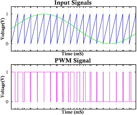
At every rising and falling slope of the triangular wave, the comparator compares the signals and generates the corresponding PWM signal. If the audio or message input is applied at the non inverting terminal of the comparator and the triangular wave is applied at the inverting terminal, the comparator will generate the PWM output signal as a pulse train of square wave having its duty cycle proportional to the amplitude of the input audio or message signal.
Figure 4. Input and output signals in a Pulse Width Modulation process.
B. Frequency Spectrum Analysis
[image:3.612.50.291.242.444.2]In an electronic system involving PWM, usually, the desired input signal has a lower frequency bandwidth while the carrier triangular wave has much higher frequency components in it. However, frequency spectrum analysis showed that, after the PWM encoding process, the output PWM signal contains frequency components both from the low frequency input signal and from the high frequency triangular signal as shown below.
Figure 5. Frequency spectrum of input and output signals throughout various stages of a PWM process. C. PWM Decoding
[image:3.612.317.565.387.481.2]It is obvious from the frequency spectrum analysis depicted above that, to decode the PWM signal and thus obtain the desired low frequency message or audio signal, one lowpass filter is enough. Choosing a lowpass filter with a suitable cutoff frequency will remove the high frequency component in the PWM signal leaving only the desired low frequency signal.
Figure 6. PWM decoding process with Lowpass Filter. Humans are capable of listening from 20 Hz up to 20 KHz of audio [6]. But, the hearing response decreases with the increasing frequency. Also, human voice and most of the musical instruments produce audio signals which can be confined pretty much in the frequency range of 30 Hz~12 KHz. Thus, to implement an audio transmission system, a lowpass filter having cutoff frequency around 10 KHz would be enough to cover most of the audio frequencies to which human ears are the most sensitive.
IV. DESIGNMETHODOLOGY
The total system of audio transmission using a visible light communication link can be divided into 3 essential sections.
[image:3.612.42.289.602.700.2]The transmitter circuit in current project is capable to deal with only single channel audio. It takes a stereo audio input from any standard music player like MP3 player, PC, Laptop etc. and converts it into mono i.e. single channel audio. The transmitter includes a triangular wave generator. Using this triangular wave and a comparator, the circuit then encodes the input audio into a corresponding PWM signal and drives two bright white LEDs with it. Thus, the emitted light also gets modulated and contains the information of the input audio.
Figure 7. Functional Block Diagram of the Transmitter.
[image:4.612.38.287.165.253.2]The stereo to mono converter uses 3 resistors to mix the 2 input audio channels into a single one. Then the audio gets amplified by an amplifier based on a collector feedback biased 2N2222A NPN transistor configuration. To generate the triangular wave, the circuit uses an integrator followed by a square wave generator, because, it is easy than direct generation of triangular wave. The square wave generator is based on a 4011 NAND gate IC with a couple of resistor and capacitors [7]. This circuit generates a square wave of 53.26 KHz frequency. Then, the integrator circuit integrates the square wave and turns it into a triangular wave. After that, this triangular wave gets amplified by a TL082 Op Amp and is fed to the comparator for PWM generation.
Figure 8. 53.26 KHz square wave with the integrated triangular wave.
For PWM signal generation, the transmitter uses a TL082 Op Amp with no feedback thus, working as a comparator. TL082 is a dual package dual power rail amplifier IC but, the current system uses only a single DC power supply. For this reason, all the input signals to TL082 must be pre-biased at half the power supply voltage [8]. The transmitter uses an LM358 Op Amp buffer circuit followed by a resistive voltage divider to generate this voltage. This voltage node is referred to as the virtual ground in the block diagram because, it acts the same way as the ground node in a dual power supply configuration.
After amplification, both the audio signal and the triangular signal are biased at the virtual ground node and then fed into the
comparator. The LED driver circuit consists of a BD135 NPN medium power transistor followed by a resistive biasing circuit. The output LEDs are connected between the positive power supply rail and the collector of BD135.
Figure 9. Circuit Diagram of the Transmitter.
Noise Removal
Scanned documents often contain noise that arises due to the accessories of printer or scanner, print quality, age of the document, etc. Therefore, it is necessary to filter this noise before processing the image. This low-pass filter should avoid as much of the distortion as possible while holding the entire signal [1, 8].
B. Transmission Channel
The transmission channel for a visible light communication system is nothing but the air in the surrounding environment. As the current project is intended to be used indoor, the possible indoor noise sources in this VLC audio transmission system channel should be considered. Usual indoor noise sources are fluorescent lamps, tungsten bulbs and CFL bulbs as they flicker at the power line frequency or other frequencies according to their driving circuitry [9]. Any kind of signal attenuation caused by the transmission channel is practically negligible in case of short range indoor transmission but the noise sources might induce some high frequency disturbances which should be filtered out at the receiver.
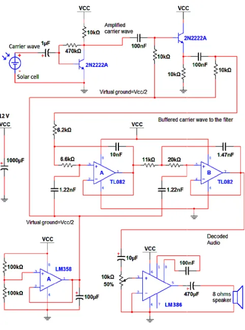
C. The Receiver Circuit
[image:4.612.41.284.428.559.2]corresponding electrical signal [10]. The receiver amplifies the electrical signal coming from photo sensor and demodulates it to obtain the original audio signal transmitted. After demodulation, power of this audio signal is amplified to make it strong enough and capable of driving a low impedance loudspeaker. This loudspeaker can be directly connected at the output of the receiver circuit to hear the audio.
[image:5.612.319.560.237.562.2]Figure 10. Functional Block Diagram of the Receiver. The Photo Sensor Module consists of a little solar cell as the light sensing element and a convex lens. They are mounted in a tube made with hard paper where the solar cell is at the focal point of the convex lens. This lens focuses the incident light coming from long distance onto the solar cell which gives maximum possible received signal strength.
Figure 11. The Photo Sensor Module.
Sensitivity of the Photo Sensor shown above, decreases with increasing frequency. So, it can’t capture higher frequencies very well. Amplitude of the generated signal is very low so, amplification is needed.
Figure 12. Electrical signal generated by the Photo Sensor. After obtaining electrical signal from the Photo Sensor, the receiver circuit amplifies it with a 2N2222A NPN transistor based amplifier. Due to having low strength, this signal can’t tolerate further loading. That’s why it goes through a common collector buffer stage made of another 2N2222A transistor[11]. Then it gets biased at half the power rail voltage and is fed to the
[image:5.612.39.284.358.442.2]next stage. This stage is obviously a PWM demodulator which recovers the transmitted audio. As said before, a lowpass filter can do this job. The current circuit uses a 4th order Butterworth Lowpass Filter having a cutoff frequency of 8 KHz [12]. This covers most of the frequency components a human ear is highly sensitive to. At 53.26 KHz, the employed filter design has attenuation of 68dB. So, the high frequency carrier signal gets highly suppressed which induces less noise into the audio. The 4th order Butterworth Lowpass Filter used in the receiver consists of two Op Amps from a TL082 IC. Thus, they also need a virtual ground node just like in the transmitter circuit. This node biases the signal at different stages of the receiver circuit. It has the same construction as in the transmitter circuit.
Figure 13. Circuit Diagram of the Receiver.
[image:5.612.40.285.523.643.2]Figure 14. 1 KHz demodulated sine wave from receiver output.
D. Circuits on Printed Circuit Board
[image:6.612.40.287.61.181.2]The pictures below present actual circuits of the transmitter and the receiver on Printed Circuit Board (PCB).
[image:6.612.37.284.275.390.2]Figure 15. Transmitter Circuit on PCB with the output LEDs.
Figure 16. Receiver Circuit on PCB with the Photo Sensor and the Speaker.
V. CONCLUSION
The VLC Audio Transmission System discussed in this document is capable of transmitting single channel audio signal with a satisfactory quality within a short range. Both of the transmitter and the receiver circuit can operate from +5V to +15V DC power supply. As, the 4th order Butterworth lowpass
filter is capable of suppressing the carrier signal by 68dB, the receiver provides with a nice quality sound. During testing, two big white LEDs having a diameter of 10mm were used. The tested indoor transmission range of this VLC Audio Transmission System with satisfactory audio quality was found to be 5 meters.
The currently implemented system has scopes to be developed further. The transmission range of this system can be increased while maintaining the audio quality. The receiver can be made more sensitive so that, it can gather information from scattered or reflected less intense modulated light. Output power of the transmitter can be increased to increase the transmission range. The system can be modified to make it capable of transmitting multi channel audio and high speed digital data.
REFERENCES [1] [1] http://www.oledcomm.com/LiFi.html
[2] Gandhi, O.P., G. Lazzi and C.M. Furse, "EM Absorption in the Human Head and Neck for Mobile Telephones at 835 and 1900 MHz," IEEE Trans. on Microwave Theory and Techniques, 44 (10), pp.1884-1897 (1996). [3] http://en.wikipedia.org/wiki/Persistence_of_vision
[4] B. P. Lathi, “Modern Digital And Analog Communication Systems”, third edition, Oxford University Press, Chapter – 6.
[5] Martin Plonus, "Electronics and Communications for scientists and engineers", Elsevier Inc., Chapter - 6Coughlin, Frederick F.Driscoll, “Operational Amplifiers & Linear Integrated Circuits”, Fifth edition, Chapter – 4.Robert F.
[6] Steven W. Smith, Ph.D., The Scientist and Engineer's Guide to Digital Signal Processing, California Technical Publishing, Chapter – 6.
[7] http://www.electronics-tutorials.ws/waveforms/generators.html
[8] Robert F.Coughlin, Frederick F.Driscoll, “Operational Amplifiers & Linear Integrated Circuits”, Fifth edition, Chapter – 3.
[9] http://www.lightsearch.com/resources/lightguides/ballasts.html
[10] A. Goetzberger, V.U. Hoffmann, “Photovoltaic Solar Energy Generation”, Chapter – 1.
[11] Robert L. boylestad and louis nashelsky, “Electronic Devices and Circuit Theory”, 7th edition, Chapter – 3.
[12] Robert F.Coughlin, Frederick F.Driscoll, “Operational Amplifiers & Linear Integrated Circuits”, Fifth edition, Chapter – 11.
AUTHORS
First Author ––Jawad Tahmeed Bin Taufik, Electrical Engineering, University of Rostock, Germany
Second Author – Mohammad Liton Hossain, Lecturer, Department of ECE, IST
litu702@gmail.com +8801768346307