32-Bit NxN Matrix Multiplication: Performance Evaluation
for Altera FPGA, i5 Clarkdale, and Atom Pineview-D Intel
General Purpose Processors
Izzeldin Ibrahim Mohd
Faculty of Elect. Engineering, Universiti Teknologi Malaysia,
81310 JB, Johor
Chay Chin Fatt
Intel Technology Sdn. Bhd.,PG9 (Intel U Building), Bayan
Lepas,11900 Penang
Muhammad N. Marsono
Faculty of Elect. Engineering, Universiti Teknologi Malaysia,
81310 JB, Johor
ABSTRACT
Nowadays mobile devices represent a significant portion of the market for embedded systems, and are continuously demanded in daily life. From the end-user perspective size, weight, features are the key quality criteria. These benchmarks criteria became the usual design constraints in the embedded systems design process and put a high impact on the power consumption. This paper survey and explore different low power design techniques for FPGA and processors. We compare, evaluate, and analyze, the power and energy consumption in three different designs namely, Altera FPGA Cyclone II which has a systolic array matrix multiplication implemented, i5 Clarkdale, and Atom Pineview-D Intel general purpose processors, which multiply two nxn 32-bit matrices and produce a 64-bit matrix as an output. We concluded that FPGA is a more power and energy efficient on low matrix size. However, general purpose processor performance is close to FPGA on larger matrix size as the larger cache size in general purpose processor help in reducing latency. We also concluded that the performance of FPGA can be improved in terms of latency if more systolic array processing elements are implemented in parallel to allow more concurrency.
General Terms
Computational Mathematics
Keywords
FPGA, Matrix Multiplication, General Purpose Processor, Systolic Array, Energy Consumption
1.
INTRODUCTION
With drastic improvement and mature of Field Programmable Gate Array (FPGA) technology nowadays, FPGAs become one of the choices for designer other than traditionally solution such as general purpose processor and digital signal processor (DSP). Its nature of reconfigurable and can be programmed to implement any digital circuit make it a best candidate for most of data computation extensive application. This is including area such as signal processing and encryption engine which involves large amount of real time data processing. FPGAs provide better throughput and latency since it is able to be customized to optimize the execution of particular process or algorithm.
Traditionally, research of FPGAs and improvement of FPGAs are mainly focusing on reducing the area overhead and increasing the speed [7-11]. With emerging of portable and mobile devices which are now become a need of most of people today, performance metrics of any of devices are not
mainly focus on latency and throughput but energy efficiency is key factor as well. As summary, performances of electronic devices are not mainly focusing on just speed but energy efficiency should be listed as a major design consideration. Designers are focusing on producing high throughput solution while maintaining the power consumption low.
A lot of study and experiment had been done comparing the energy efficiency between FPGAs, DSPs, embedded processor [1] and general purpose processor. However, particularly on general purpose processor, most of experiment are not comparing to the greatest and latest commercial processor in market which claimed by manufacturer that several low power design techniques had been adopted. With the advance of semiconductor process technology nowadays which lead to lower leakage current, and flexibility of software implementation for power saving, performance of general purpose processor in term of power dissipation and energy consumption had greatly improved. The key question here is how well current modern general purpose processor in market performs in term of energy efficiency compares to FPGAs particularly on signal processing centric application. This paper is going to evaluate and discuss in detail this key question by executing nxn matrix multiplication on Altera Cyclone II FPGA [17-19] and Intel processor and comparing the performance of both devices in term of power dissipation and energy efficiency.
2.
RELATED WORK
consumption. Thus, accuracy of power estimation shown by Ronald Scrofano et al is a concern.
Seonil Choi et al developed an energy efficient design for matrix multiplication base on uniprocessor architecture and linear array architecture for both on chip and off chip storage [2-6]. No actual measurement was taken on actual HW implementation. However, energy consumption was estimated using Xilinx Xpower tool. They showed that linear array architecture need 49 cycles for 6x6 matrices and up to 256 cycles for 15x15 matrices.
3.
SYSTOLIC ARRAY MATRIX
MULTIPLICATION ON ALTERA
CYCLONE II
Traditional way of implementing systolic array for matrix multiplication is matching the systolic array order to the problem size [12-16]. For example, an 8x8 matrix size will need 8x8 order systolic array and 16x16 matrix size will need 16x16 order systolic array. The basic building block of systolic array is 2x2 and each 2x2 systolic array need 4 multiply and accumulators (MAC) as shown in Figure 1. The number of MAC increases tremendously if problem size increases. Table 1 below shows number of MACs required on matrix size.
Table1: Resource utilization on difference Matrices sizes
Matrix Size Number of 2x2 systolic array
Number of MACs
2x2 1 4
4x4 4 16
8x8 16 64
16x16 64 256
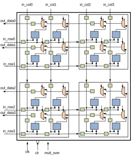
[image:2.595.321.534.76.290.2]Our target FPGA device for power measurement is Cyclone II EP2C35F672C6 which has only 33,216 logic elements and 70 embedded 9 bits multiplier. Besides, input data of 32 bit and output data of 64 bit imply that we need pretty huge MAC on wide bus width. If we follow the method of matching the matrix size to the order of systolic array, resource utilization will exceed the number of gate on target devices. Alternatively, we utilized 4x4 systolic arrays which is developed by connecting four 2x2 systolic arrays in the way shown in Figure 2, as basic building block to construct up to 16x16 matrix multiplication. In other words, the same 4x4 systolic arrays will be used to implement 2x2, 4x4, 8x8 and 16x6 matrix multiplication module on the expense of latency increment on larger problem size. Figure 3 below illustrates the implementation with single 4x4 systolic array.
Figure 1: Functional Block Diagram of 2x2 Systolic Array
Figure 2: Functional Block Diagram of 4x4 Systolic Array
Clearly, an algorithm is needed in order to use a single 4x4 systolic array for all matrices sizes. The steps below show the method of constructing 8x8 matrix multiplication module from a single 4x4 systolic array.
Step 1: Divided an 8x8 input matrix A and matrix B to four 4x4 sub matrices which are named as A1-A4 and B1-B4.
MAC MAC
MAC MAC
1
0
1
0
1
0
1
0 Reg
Reg Reg
Reg Reg
Reg Reg
Reg Reg
Reg
in_col0 in_col1
in_row0
in_row1
out_row0
out_row1 in_data0
in_data1
out_col0 out_col0
out_data0
out_data0
mult_over
mult_over mult_over
mult_over
mult_over clk clr
clk clr mult_over
in_col0 in_col1 in_col2 in_col3
in_row0
in_row1
in_row2
in_row3 out_data0
out_data1
out_data2
[image:2.595.322.541.325.587.2]Step 2: Output matrix C can be obtained by passing sub matrix A and sub matrix B to 4x4 systolic array and adding up the result accordingly as below
[image:3.595.53.285.166.524.2]C1= A1xB1+A2xB3 C2= A1xB2+A2xB4 C3= A3xB1+A4xB3 C4= A3xB3+A4xB4
Figure 3: Implementation of matrix multiplier with single 4x4 systolic array
[image:3.595.316.550.196.429.2]The same method can be used for higher matrices sizes such as 16x16. As example, for 16x16 matrix size, we first need to divide the input matrix to four 8x8 sub matrices. And, each 8x8x sub matrix will be further divided into four 4x4 sub matrices. Figure 4 below illustrates the method of constructing 8x8 matrix multiplication module from a single 4x4 systolic array
Figure 4: Constructing 8x8 matrix multiplier from single 4x4 systolic array
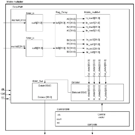
Figure 5 shows the high level functional block diagram of overall design. Both 32 bit matrix A and matrix B will be stored in Random Access Memory (RAM). A module (Reg_delay) is required to stagger the input matrix A and matrix B as required by algorithm of systolic array. A 4x4 matrix multiplication module responsible to compute the multiplication between elements of matrix A and matrix B. Dataout module responsible for addition of result of 4x4 matrix multiplication and write each element of output matrix to RAM_out. Output of matrix multiplication result will be stored in RAM.
Figure 5: High Level Functional Block Diagram of Matrix Multiplication Module
4.
MATRIX MULTIPLICATION ON
GENRAL PURPOSE PROCESSOR
For general purpose processor, we used Intel i5 Clarkdale Intel Atom Pineview-D processor. Matrix multiplication is running on MATLAB on these two processors. MATLAB was used because it is incorporates the Linear Algebra Package (LAPACK) which greatly improve the performance of matrix multiplication. A single iteration of computation of matrix multiplication will not take advantage of the large cache size in Intel processor. Thus, in order to utilize the cache from Intel processors, 1000 iterations of 32 bit matrix multiplication will be executed. With this, we can ensure that the cache in processor will be fully utilized.
5.
POWER AND ENERGY
MEASUREMENTS
Power is measured using Tektronix current probe with current amplifier and digital Tektronix digital oscilloscope TDS7104 to capture both the current and the voltage.
The power is obtained by multiplying the voltage and the current. Average voltage and current are measured within the window of matrix multiplication process. The energy consumption is obtained by multiplying the average power to total execution time.
2x2
2x2 2x2
2x2 2x2
2x2 Multiplier
2x2 Multiplier
4x4 Multiplier
4x4 Multiplier
8x8 Multiplier
8x8 Multiplier 16x16 Multiplier16x16 Multiplier
8x8 8x8
8x8 8x8 4x4 4x4
4x4 4x4
Resources Intensive !!!
Resources Intensive !!!
2x2
2x2 2x2
2x2 2x2
2x2 2x2
2x2 2x2 2x2 2x2
2x2 2x2
2x2 Multiplier
2x2 Multiplier
4x4 Multiplier
4x4 Multiplier
8x8 Multiplier
8x8 Multiplier 16x16 Multiplier16x16 Multiplier
With Scheduling
With Scheduling
A1 A2
A3 A4
B1 B2
B3 B4
X
MatrixA 8x8 MatrixB 8x8
C1 C2
C3 C4
=
MatrixC 8x8
A1B1+A2B3 A1B2+A2B4
[image:3.595.54.295.646.735.2]5.1. Power and Energy Measurements on
ALTERA DE2 Board
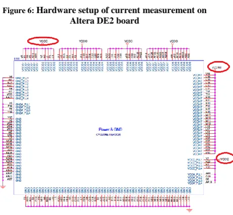
[image:4.595.324.545.69.237.2]Figure 6 shows the experiment setup for the power measurement on ALTERA board. The Cyclone II Altera FPGA (EP2C35F672C6) is powered by 3 power rails. There are the core voltage (VCC_INT, 1.2V), IO Voltage (VCCIO, 3.3V) and PLL Voltage (VCC12, 1.2V). Figure 7 below shows the power supply pins of the Cyclone II FPGA. In order to obtain total power consume by the entire IC, the current drawn by each of those rail is measured.
Figure 6: Hardware setup of current measurement on
[image:4.595.57.284.191.324.2]Altera DE2 board
Figure 7: Power Supply Pins of Cyclone II EP2C35F672C6
IO voltage (VCCIO) of Cyclone II is power directly by 3.3V rail on Altera DE2 board through a 0ohm resistor (R92) as shown in Figure 8. So that, the current drawn by Cyclone II can be easily measure by replacing the 0ohm resistor with a wire loop for current probe to be clamped on.
Both core voltage and PLL voltage are connected to output of a low dropout regulator (LDO). Since there is no shunt resistor exist on the output of LDO, a workaround is needed to measure the power consume by these 2 voltage rails. In order to measure the current on both voltage rails, output pin (pin 2) of LDO (U24) have been lifted up and a wire loop is inserted for current probe to be clamped on as shown in Figure 8. The current is measured at the output of the LDO but not the input of the LDO to exclude the efficiency loss of the LDO. If we measured the current at the input of the LDO, it includes the efficiency loss of LDO which is not required.
Figure 8: Power Block of ALTERA DE2 Board
5.2 Power and Energy Measurements on
the General Purpose Processors
In the computer system, the power supply unit is supplying 5V, 3.3V and 12V to the motherboard. 12V is the main voltage used by processor switching voltage regulator. 12V to processor is supplied through a 2x2 or 2x4 power connector from power supply. 12V input will be down regulated to processor core and IO voltage. Thus, measuring the 12V input current from 2x2 or 2x4 power connector will give the total current consume by processor.
Since the computer system is running on operating system and there are other background activities which will consume processor resources, we have to take into consideration current consumes by those background activities. Otherwise, current measure will not only included the current consume by matrix multiplication process but it include other process that is happening in background as well. One of the ways to overcome this is to measure the current on 12V rail when system is idle. Idle is referring to situation where system is power up but no other active process is running on the system except those background activities initiate by operating system. And another set of current measurement is taken when system is running the required matrix multiplication routine. By subtracting the idle current from the current consume during matrix multiplication routine, we can obtain the net current used just to execute the matrix multiplication. With this methodology, we can measure both the power and energy consume by processor for the particular matrix multiplication module as shown in Figure.9.
[image:4.595.63.294.329.542.2] [image:4.595.319.543.596.739.2]6.
RESULTS AND ANALYSIS
In this section, we analyzed the results of power and energy we obtained from both Altera DE2 board as well as the two platforms with Intel Core i5 and Intel Atom Pineview-D processor. We discussed the observation we have from result obtained. All measurements are done on 1000 iterations of matrix multiplication on the three different designs.
6.1. Power
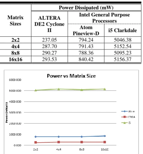
From the results shown in Table 2 and Figure 10, it is cleared that FPGA dissipate the least amount of power compared to Intel i5 Clarkdale and Intel Atom Pineview-D. Our result shows that Intel Atom Pineview-D perform better in term of power dissipation compare to Intel i5 Clarkdale so that Intel Atom series can be used for low power application. Intel Core i5 consumes 16 times as much as power compare to Altera Cyclone II while Intel Atom consumes 2.6 times more power than Cyclone II.
[image:5.595.314.545.217.319.2]Apparently, an interesting observation to be noted is all of three implementations are consuming the same amount of power regardless of matrix size. This is due the same HW unit will operate at any case regardless of problem size and data content.
Table 2: Power Dissipation versus Matrix Sizes for the three Implementations
Matrix Sizes
Power Dissipated (mW)
ALTERA DE2 Cyclone
II
Intel General Purpose Processors Atom
Pineview-D i5 Clarkdale
2x2 237.05 794.24 5046.38
4x4 287.70 791.43 5152.54
8x8 290.27 788.36 5095.23
16x16 293.53 840.42 5156.37
Figure 10: Power Dissipation versus Matrix Sizes for the three Implementations
For matrix multiplication on the FPGA, we used single 4x4 systolic array as basic building block for all matrix size as we stated earlier in previous section. That is the reason why we got same amount of power dissipated on all matrix sizes. As the result we can concluded that for higher order of systolic array, the power consumption will increase by the same amount of logic element increment. For example, if we choose to use 8x8 systolic array as basic building block, the amount of power dissipated on FPGA will become closer to
Intel Atom Pineview-D. However, this will come with advantage of reducing the latency.
6.2 Energy
A device with less power dissipation doesn’t mean that it has longer battery time. It might dissipate less power but take significant time to complete a task compare to a high power dissipation device but operate faster. A more accurate measurement on battery life is using energy. Energy can be calculated by multiplying average power to latency.
Table 3: Energy Consumption versus Matrix Sizes for the three Implementations
Matrix Size
ALTERA DE2 Cyclone II
Intel General Purpose Processors Atom
Pineview-D
i5 Clarkdale
Latency (ms)
Energy (mJ)
Latency (ms)
Energy (mJ)
Latency (ms)
Energy (mJ)
2x2 0.25 0.06 13 10.33 1.80 9.08
4x4 1.14 0.33 13.8 10.92 2.20 11.34
8x8 7.76 2.25 19 14.98 2.50 12.74
16x16 60.02 17.62 41.4 34.79 3.90 20.11
As shown in Table 3 and Figure 11.The ALTERA FPGA is consumed the least energy for matrix size up to 16x16. However, on matrix size higher than 16x16, a linear extrapolation on the line graph will reveal that Intel Core i5 performs better than FPGA in terms of energy consumption. The main reason is the latency of FGPA implementation increases at rate higher than the latency increment rate of Intel Core i5 when matrix size grows from 16x16. The scheduling we made on FPGA design in order to reduce resource utilization is the main reason of excessive latency increment. One can reduce the latency by using higher order of systolic array as basic building block. Apparently, Intel Atom is not an economic solution for matrix multiplication centric application. Even though Intel Atom dissipates less power than Intel Core i5 but overall it consumes more energy than Intel Core i5 on same workload. However, we not deny that minimum power dissipation is still important to keep minimum heat dissipation for simple thermal solution.
[image:5.595.49.288.366.624.2]On other hand, if we increase the order of systolic array in the way that it matches with problem size, latency will improve significantly. For example, use 16x16 systolic array for problem size of 16x16. In order to estimate the energy consumption, we have to understand the resource utilization increment as well as the latency improvement if higher order of systolic array is used.
[image:5.595.317.545.607.742.2]A 4x4 systolic array is formed from four 2x2 systolic array, an 8x8 systolic array is constructed from four 4x4 systolic array and so on. With scheduling, we use single 4x4 systolic array for problem size of 8x8. Now, without scheduling we need four 4x4 systolic array on problem size of 8x8. Thus, in term of resource utilization, it increases by factor of 4. Furthermore, if we assume that power dissipation is proportional to resource utilization, power dissipation will increase by factor of 4 as well.
[image:6.595.55.282.290.438.2]As for the latency, matrix size of 8x8 needs 8 iterations if single 4x4 systolic array is used. However, four 4x4 systolic array will reduce the latency by factor of 8. Thus, overall energy consumption will be reduced by 50% (power dissipation increases by 4 times but latency decrease by 8 times). Figure 12 shows that the estimated energy consumption if order of systolic array is matching with matrix size. If we linearly extrapolate the line graph, FPGA is still the candidate consume the least energy even at matrix size higher than 16x16.
Figure 12: Energy consumption versus matrix size with estimated result on higher order systolic array
7.
CONCLUSION
Due to hardware limitation on Altera DE2 with Cyclone II EP2C35F672C6 which only has 33,216 logic elements, systolic array matrix multiplication design has to be scheduled and using only 4x4 systolic array. This approach helped to ensure that design can be implemented and fit into Altera DE2 board. However, it induces significant latency. This design can be modified with higher order of systolic array to minimize latency and implement on FPGA family with higher logic count such as Cyclone IV EP4C115 which has 115,000 logic elements.
Using more resources for parallel processing will always reduce the latency but it increases the power dissipation. This is because a powerful chip required more silicon area as more circuit is required. Comparing between Atom Pineview-D and Core i5, obviously Core i5 has better performance but it suffer for higher power dissipation. For matrix size less than 16x16, we observed the FPGA is the best candidate in term of power and energy consumption. Increasing the matrix size further to greater than 16x16, Core i5 become a more favorable candidate. Larger data and instruction cache in Core i5 is the main reason we do not see latency increase at rate as high as on Atom Pineview-D and Cyclone II when matrix size increase. However, if we increase the order of systolic array to match the matrix size, our estimated result show that FPGA is still the most economical candidate for matrix multiplication.
8.
ACKNOWLEDGMENTS
We would like to thank the Universiti Teknology Malaysia for funding support. We also like to take this opportunity to express our appreciation to the Intel Technology SDN BHD Malaysia, In particular, Intel Test and Tool Operation (iTTO) for making this work possible.
9.
REFERNCES
[1]. R. Scrofano, S. Choi, and V. K. Prasanna, “Energy Efficiency of FPGAs and Programmable Processors for Matrix Multiplication,” in Proc. of IEEE Intl. Conf. on Field Programmable Technology, pp. 422-425, 2002.e [2]. S. Choi, V. K. Prasanna, and J. Jang, “Minimizing
energy dissipation of matrix multiplication kernel on Virtex-II,” in Proc. of SPIE, Vol. 4867, pp. 98-106, 2002.
[3]. J. Jang, S. Choi, and V. K. Prasanna, “Energy efficient matrix multiplication on FPGAs,” in Proc. of 12th Intl. Conf.on Field Programmable Logic and Applications, pp. 534-544, 2002.
[4]. J. Jang, S. Choi, and V. K. Prasanna, “Area and Time Efficient Implementations of Matrix Multiplication on FPGAs,” in Proc. of IEEE Intl. Conf. on Field Programmable Technology, pp. 93-100, 2002.
[5]. H. T. Kung and C. E. Leiserson, “Systolic arrays for (VLSI),” Introduction to VLSI Systems, 1980.
[6]. V. K. P. Kumar and Y. Tsai, “On synthesizing optimal family of linear systolic arrays for matrix multiplication,” IEEE Trans Comput., vol. 40, no. 6, pp. 770–774, 1991. [7]. Lamoureux J and Luk, W,“An overview of Low-Power
Techniques for Field-Programmable Gate Arrays.”, in Adaptive Hardware and System. AHS’08. NASA/ESA, 2008.
[8]. Sutter, G., Boemo, E. "Experiments in low power FPGA design", Lat. Am. Appl. Res., vol.37, no.1, pp.99-104, 2007.
[9]. Dave. N, Fleming. K, Myron King, Pellauer. M, Vijayaraghavan, M. “Hardware Acceleration of Matrix Multiplication on a Xilinx FPGA”, in Formal Methods and Models for Codesign, 2007. MEMOCODE 2007. 5th IEEE/ACM International Conference, May 30 2007-June 2 2007.
[10].Aslan. S, Desmouliers. C., Oruklu. E and Saniie. J. “An Efficient Hardware Design Tool for Scalable Matrix Multiplication”, in Circuits and Systems (MWSCAS), 2010 53rd IEEE International Midwest Symposium, pp1262-1265, 2010
[11].H.T. Kung. “Why Systolic Architecture”, in IEEE computer, pp37-46. 1982
[12].Ju-Wook Jang, Seonil B. Choi and Viktor K. Prasanna. “ Energy and Time Efficient Matrix Multiplication on FPGAs”, in IEEE transactions on very large scale integration (VLSI) system vol 13, NO 11, November 2005.
[14].Syed M, Qasim, Ahmed A.Telba, Abdulhameed Y. AlMazroo. “FPGA Design and Implementation of Matrix Multiplier Architectures for Image and Signal Processing Applications”, in IJCSNS International Journal of Computer Science and Network Security, VOL 10. NO2, Feb 2010.
[15].AHM Shapri and N.A.Z Rahman. “Performance Analysis of Two-Dimensional Systolic Array Matrix Multiplication with Orthogonal Interconnections”, in International Journal on New Computer Architectures and Their Applications (IJNCAA) 1(3): 1090-1100, 2001
[16].Jonathan Break. “Systolic Array and their Application”, inhttp://www.cs.ucf.edu/courses/cot4810/fall04/.../Systol ic_Arrays.ppt
[17].Altera Inc, Cyclone II Device Handbook, Volume 1, available at www.altera.com
[18].Altera Inc, DE2 Development and Education Board Use Manual available at www.altera.com