An Enhanced Automatic Surface and Structural Flaw
Inspection and Categorization using Image Processing
Both for Flat and Textured Ceramic Tiles
Md. Maidul Islam
World University of Bangladesh(WUB), Dhaka, Bangladesh
Md. Rowshan Sahriar
Gononet Online SolutionsDhaka, Bangladesh
Md. Belal Hossain
Atish Dipankar University ofScience and Technology (ADUST), Dhaka, Bangladesh
ABSTRACT
As the price of ceramic tiles depend on its limpidness and precision of surface texture, color and shape, it’s in fact a great challenge to control surface eminence and uphold production rate in the field of industrial fabrication of ceramic tiles. Under consideration these criteria, in this research paper, we have proposed an enhanced automatic surface flaw detection and categorization procedure that is able to guarantee the quality of ceramic tiles as well as production rate in industrial fabrication. Our proposed model plays an important role for automatic revealing of surface flaw during production and packaging. This proposed model includes an automatic categorization technique using computer vision that helps us to make sense about the pattern of surface defect within a very short time and also helps to make quick decision about the recovery process. Moreover, it also ensures the quality of tiles automatically during packaging procedure so that the defected tiles may not be mixed up with the fresh tiles.
Keywords
Quality Control, Surface and Structural Flaw, Pattern of Defect, Flat and Textured Tiles.
1.
INTRODUCTION
As technology advances, image processing is one of the ever-increasing areas in computer science. From space science to our daily life, everyday huge amount of images are to be captured. However, it is quite difficult to process or handle those images manually within a short period of time. So the concept of digital image processing with computer vision is growing rapidly which is used to extract various features automatically from images. After extraction of features from image, knowledge based technique is to apply for taking recovery scheme from those extracted features with the help of computer and without or with a little human intervention as well.
One of the most significant research areas of digital image processing is to identify and classify various kinds of defects from 2D or 3D images captured by real time sensor or camera. Therefore, to identify the defect and its pattern from any image, there are several techniques are sited and deployed at three levels. Lowest levels of this technique are deal with the raw, perhaps noisy pixel values, with de-noising and edge detection procedure being good examples. Middle level deploys with algorithms which utilize low level results, for instance, segmentation and edge-linking. At the highest level of this technique cope with those methods which attempt to extract semantic meaning from the information provided by the lower level.
Nowadays, ceramic tile manufacturing industry is a prominent and up growing sector. All phases of the production cycle are maintained and controlled technically awaiting the final phase of the manufacturing process come into view, i.e. packaging. Before packing, it is important to make sure of defect less for maintaining quality of ceramic tiles (i.e. whether checking broken tiles, spotted tiles). So it is a vital task to classify the ceramic tiles after production based on surface defects. Defect inspection through manual procedure is labor intensive, time-consuming and subjective as well.
Although automated defect detection method have been deployed in ceramic tiles industries since few years but there still have complex procedure to classify defects using human vision i.e. automated classification and grading mechanism of packing have not been implemented yet. Again human judgment may be inclined by anticipation and aforementioned to awareness. In fact, most inexperienced observers have the same opinion that the flaw may have still there, when they cannot classify the structure of tiles properly. Such a monitoring task is naturally wearisome, prejudiced and costly in terms of production environment.
Objective of this research paper is to propose an efficient surface flaw inspection and categorization procedure which will be able to uncover the surface defects of ceramic tiles at a high rate within a dumpy time.
Organization of this study is as follows. Section 2 describes briefly about previous study. Section 3 illustrates our projected method. Section 4 represents the tentative results and evaluation. At last, a noteworthy conclusion is presented in Section 5.
2.
EXISTING METHODS FOR DEFECT
DETECTION
Since last decade, some defect inspection mechanisms have been proposed to identify the surface flaw of industrial products (i.e. ceramic tiles, steel bar and wooden surface) by capturing their real time surface image. Their proposal can be described briefly as follows:
rather it emphasizes on the human visual inspection of defect classification in industrial environment. Moreover, this system is suffered by redundant operation since they apply the second portion on every test image to identify and classify various types of defects. Thus this system is time consuming as well.
C. Boukouvalas et al. [4], they applied separable line filters for flat tiles to identify crack and pinhole defects. Again, they applied winger distribution for crack detector and a novel conjoint spatial-spatial frequency representation for textured tiles. In terms of color textured tiles, this type of detection algorithm which looks for abnormalities both in chromatic and structural properties. However, use of separate filtering technique for identifying distinct defect is not a good practice. Consequently, high computational time is taken while we are to handle a large number of operations during production time. It also proceeds with visual defect classification with human intervention.
Se Ho Choi et al. [5] applied a real time mechanism for surface flaw detection of steel coil and bar in high speed production environment. They used a scheme named “edge preservation” for noise cutback and performance improvement. In addition, they used “second derivative laplacian” filter to differentiate gray scale images from each other. Finally, they applied “double thresholding” technique to formulate binary images. Still, this type of technique is unable to find the orientation of the edge of surface, because they use “second derivative laplacian” filter which malfunctions for corner and curves flaw detection as well [10]. In contrast, they hadn’t developed any automatic classification mechanism rather it was also a human vision process to classify the surface flaw.
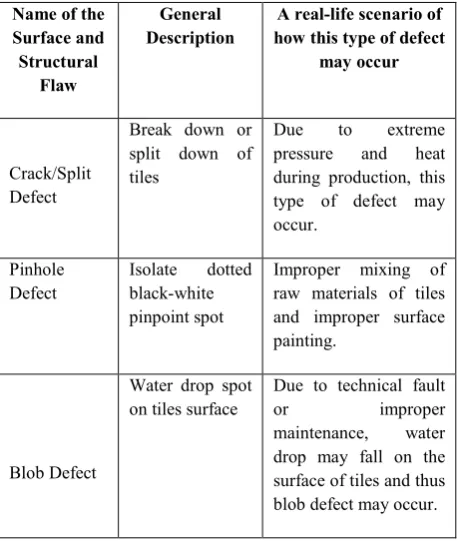
[image:2.595.314.543.71.352.2]After thoroughly revision of previous research paper, there may exists eight types of defects which may occur during production time and/ or packaging time. The category of surface and structural defects are shown in Table 1.
Table 1. Types of surface and structural defect
Name of the Surface and Structural
Flaw
General Description
A real-life scenario of how this type of defect
may occur
Crack/Split Defect
Break down or split down of tiles
Due to extreme pressure and heat during production, this type of defect may occur.
Pinhole Defect
Isolate dotted black-white pinpoint spot
Improper mixing of raw materials of tiles and improper surface painting.
Blob Defect
Water drop spot on tiles surface
Due to technical fault
or improper
maintenance, water drop may fall on the surface of tiles and thus blob defect may occur.
Spot/ Blemish Defect
Discontinuity of paint or shade on surface [7].
This type of defect may occur by falling water drop or by color discontinuity on the surface.
Corner/ Bend Damage
Split or crack down of corner of tiles
Due to extreme pressure and heat during production, this type of defect may occur.
Edge/ Border Damage
Break down of edge of tiles
Scratch Effect
Generally graze on surface of tiles
Due to fiction between surface and mechanical equipment during production time.
Glaze Effect
Hazy and
unclear surface of tiles
Cause of this defect is improper color mixing and painting on surface or having scratch on surface.
3.
PROPOSED APPROACH OF DEFECT
DETECTION AND CLASSIFICATION
3.1
Introduction
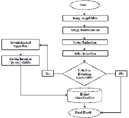
A new surface defect detection and classification method has been proposed by this section. Our proposed method consists of two major portions. One includes some pre-processing image operations to contrast features. And another portion includes some prominent feature extraction operations to identify defects and to classify those defects as well.
Our proposed model also introduces several algorithms by which we can boost up the system performance at a higher rate than existing one during production time. Thus it also can reduce the computational time all together. Here, we applied our mechanisms step-by-step on ceramic tiles image which is captured before by a digital camera. Table 2 entails operations that we performed on captured image of ceramic tiles.
Table 2. Proposed three layer approaches for surface flaw detection and classification
PROPOSED SURFACE FLAW DETECTION AND CATEGORIZATION PROCESS
Levels of Application
Process Description
First Step First step focuses on performing several image preprocessing operations on captured tiles image.
[image:2.595.53.282.484.755.2]Third Step Finally, we applied our defect classification algorithm on captured image to categorize all defects.
[image:3.595.56.280.174.379.2]The absolute flowchart of our proposed flaw inspection and categorization method has been rendered in the following Figure 1.
Fig 1: Flow chart of our proposed surface flaw detection and classification
3.2
First Step: Performing Some Image
Pre-processing Operations
Earlier than applying our proposed defect detection method, initially, we must make use of several image pre-processing operations on the input images. Pre-processing operations include RGB to Binary conversion, image enhancement, noise reduction etc. Pre-processing operations are imperative for renovating the captured RGB image [7].
3.2.1
Image Acquisition
The procedure of getting a digital image from a real world source is called “Image Acquisition”. After capturing a ceramic tile image, it is to store into the computer for further processing. Image capturing may be achieved by taking live photo using real time sensor during ceramic tiles production. In our method, we have used KODAK EASYSHARE P850 digital camera for image acquisition. To make all the captured images in identical dimension, images are being trimmed with m×n (width and height) dimension.
3.2.2
Image Enhancement
Image enhancement is a specific type of operation that is used to improve interpretability or perception of information in image for understanding and evaluating using human vision. For example, medical imaging, satellite imaging etc.
Another aspect of image enhancement is to make available better input for other automatic image processing operations [8]. The main goal of image enhancement is to alter one or more characteristic of captured image to make it more appropriate and reliable for a specific feature extraction. However, contrast stretching (often called normalization) is
one of the straightforward image enhancement techniques that focus to improve the contrast in an image by stretching intensity value of the captured image. Basic idea behind contrast stretching is to increase the dynamic range of intensity value of the processed image. To do so, at first, the captured image is to convert into a gray level image. The general practice of the contrast stretching operation [1] on grayscale image is to stretch the intensity value of each pixel using the following equation to form a contrasted image.
i n
y x I y x
O i +
− −
= )
min max min)( ) , ( ( ) , (
(1)
Where, O(x,y) represents the output image, I(x,y) represents the pixel position in input image. In this equation, ni correspond to the number of intensity levels, i stand for the initial intensity level, "min" and "max" represent the minimum intensity value and the maximum intensity value in the current image respectively. Here "no. of intensity levels" refers the total number of intensity values that can be assigned to a pixel. For example, normally in the gray-level images, the lowest possible intensity is 0, and the highest intensity value is 255. Thus "no. of intensity levels" is equal to 256. The contrast stretching operation is applied on the grayscale images in two passes. In the first pass the algorithm calculates the minimum and the maximum intensity values in the image, and in the second pass through the image, the above formula is applied on the pixels. In the proposed method, we enhance the gray level image to improve its visual quality and machine recognition accuracy using the following formula, described in [1]:
(
F
stretc
h
M
E
)
INTRANS
G
=
′
,
′
,
,
(2)Here, performs the intensity or gray level transformations and G computes a contrast stretching transformation using the following MATLAB expression:
(
)
(
)
(
M
F
eps
E
)
Contrast
=
1
.
/
1
+
.
/
+
.^
(3)Where, parameter M must be in range [0,1]. The default value for M is and the default value for E is 4. Here, F is gray-level image and M is such result which is found by applying image double and median filtering operation on F. eps returns the distance from 1.0 to the next largest double-precision number, i.e.
(
52
)
^
2
−
=
eps
(4)3.2.3
Noise Reduction
The term “noise” may appear in every steps of image acquisition process due to improper lighting or by using faulty camera or electronic sensor while capturing image. However, “noise” refers to inconsistent variation of pixel intensity in image which may produce unwanted additional information and complexity. As a result the actual feature of captured image may be changed which is unexpected and undesirable. However, it is not possible to get noise free image, rather noise can be reduced. Basically, Noise reduction is a process of removing noise from a captured image. To remove noise some filtering techniques [1] have been proposed as follows:
harmony with the values of its neighbors. In general, a smoothing filter sets each pixel to the average value, or a weighted average, of itself and its nearby neighbors; the Gaussian filter is just one possible set of weights. But smoothing filters tend to blur an image, because pixel intensity values that are significantly higher or lower than the surrounding neighborhood would "smear" across the area. Because of this blurring, linear filters are seldom used in practice for noise reduction.
For the above reason, we proposed to use a non-linear filter which is called median filter. It is very good at preserving image detail if it is designed properly. To run a median filter:
1. Consider each pixel in the image.
2. Sort neighboring pixels into order based upon their intensities.
3. Replace the original value of the pixel with the median value from the list.
A median filter is a rank-selection (RS) filter, a particularly harsh member of the family of conditioned rank-selection (RCRS) filters [2]; a much milder member of that family, for example one that selects the closest of the neighboring values when a pixel's value is extremely in its neighborhood, and leaves it unchanged otherwise, is sometimes preferred, especially in photographic applications.
Median filter technique is good at removing salt and pepper noise from an image, and also causes relatively little blurring of edges, and hence is often used in computer vision applications [9].
3.2.4
Edge Detection
An edge may be regarded as a boundary between two dissimilar regions in an image. These may be different surfaces of the object, or perhaps a boundary between light and shadow falling on a single surface. In principle, an edge is easy to find since differences in pixel values between regions are relatively easy to calculate by considering gradients. Every edge extraction techniques [3] are consists of two distinct phases:
1. Finding pixels in the image where edges are likely to occur by looking for discontinuities in gradients. 2. Linking these edge points in some way to produce
descriptions of edges in terms of lines and curves.
For the proposed method, we detect edge using sobel edge detection method [6] upon the resulting image. Actually there are many kinds of edge detectors. We use first derivative edge detector (sobel) to detect edges of the image. Because, it’s calculation is very simple and fast to detect edges. On the other hand, if we use second derivative edge detector operator such as laplacian of gaussian operator then we will not be able to find the orientation of the edge because of using the laplacian filter. Again, if we use other kinds of gaussian edge detectors such as canny, shen castan, boie-cox operators then the operation is more complex [9].
3.3
Applying the Proposed Defect
Detection Process
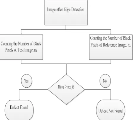
All preprocessing operations are applied to the reference image, stored in the computer database to compare with the test image. Let, the resulting image is I2. Now we consider I1 as the resulting image found from the test image after applying all preprocessing operations. We propose here a new technique. We store I1 and I2 as matrix form to a file. Let,
these two matrices are named as m1 and m2. Then we count the total number of black pixels (in binary, it is represented as 1) in m1 and that in m2. These two are then compared. If the number of black pixels in m1 is greater than the number of black pixels in m2 then we can make decision that defect is found in the test image, otherwise we can say that no defect is present to the test image. To understand this concept clearly, consider the following example:
Let, we have a test image and a reference image of equal size. Now applying preprocessing steps on the test image we find matrix m1 whose value is:
0 1 0 0 0 1 0 1 0 0 0 0 0 0 0 0 0 1 0 0 0 1 0 0 1
Again, applying the preprocessing operations on the reference image another matrix m2 is found:
0 0 0 0 0 0 0 0 0 0 0 0 0 0 0 0 0 1 0 0 0 0 0 0 1
[image:4.595.319.544.415.617.2]Here, the number of black pixels for the reference image is 2 and for the test image this number is 6. So, here obviously 6>2 and we can make decision that defect is found on the test image. The detailed block diagram of the proposed defect detection step is shown in the following Figure 2.
Fig 2: Flow chart of our proposed surface flaw detection (Second step)
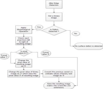
3.4 Defect Classification Using Our
Proposed Algorithms
basic building blocks of initial operations for flat tiles defect inspection.
STEP: 1. After finding the binary image, apply morphological operation on it.
STEP: 2. Now check each pixel elements of resulting image from left to right.
STEP: 3. If any pixel element has value ‘1’ then change its value to ‘2’.
STEP: 4. Change such co-ordinates of binary image as ‘2’ which of the resulting image have value ‘2’.
[image:5.595.320.539.72.261.2]STEP: 5. Finally, save this resulting matrix into a text file.
Fig 3: Flow chart of initial operations for flat tiles
3.4.1.2 For Textured Tiles
STEP: 1. Save these coordinates of reference image after checking and if any of its coordinates has value ‘1’.
STEP: 2. Convert the test image into binary, after that apply morphological operation on it.
STEP: 3. Now check each pixels of resulting image from left to right.
STEP: 4. If any pixel has value of ‘1’ then change its value to ‘2’.
STEP: 5. Change such co-ordinates of binary image as ‘2’ which of the resulting image have value ‘2’.
STEP: 6. Convert the previous saved coordinate values of binary test image as ‘0’.
STEP: 7. Finally, save this resulting matrix into a text file.
Flow chart of initial operations that must be applied before going to start of surface and structural flaw detection and classification for textured tiles indicates in Figure 4.
Fig 4: Flow chart of initial operations for textured tiles
3.4.2 Algorithm to Determine Pinhole Defects
Let, p_count as a variable for pinhole count, c_range as the range of corner, e_range as the range of edge and row as the maximum number of image pixels along any row and colas the maximum number of image pixels along any column. Figure 5 indicates the basic flow chart for pinhole detection.STEP: 1. Set, temp_a =c_range, and temp_b=e_range. STEP: 2. Divide the total searching area for pinhole into three regions i.e. left, right and middle.
STEP: 3. For left side region,
For row consider the range from temp_a+1 to row-c_range-1 For column consider the range from temp_b+1 to c_range (a) Check each pixel values whether it is ‘0’ or not.
(b) If it is true then (i) for each coordinate (i, j) check all of its eight neighbors. (ii) If (i, j-1), (i, j+1), (i-1, j), (i+1, j) position values are ‘1’ and the rest are ‘0’, then p_count will be incremented by 1.
[image:5.595.55.281.115.397.2]STEP: 4. For right side region, range for row is from temp_a+1 to row-c_range-1 and range for column is from col-temp_a+1 to col-e_range. The rests are same as STEP 3. STEP: 5. For middle side elements, range for row is from temp_b+1 to row-e_range and range for column is from col-temp_a+1 to col-c_range. The rests are same as STEP 3. STEP: 6. Finally, check value of p_count. If p_count>0, then pinhole is found, otherwise not found.
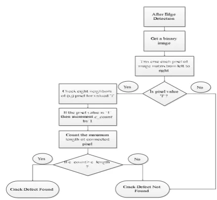
[image:5.595.321.534.560.743.2]3.4.3 Algorithm to Determine Crack Defects
Let c_length as the range of crack. Figure 6 shows the operation performed for crack detection.STEP: 1. Check every pixel coordinate (i, j) from left to right up to the last pixel element.
STEP: 2. If any (i, j) has value ‘1’ then
(a) Consider its adjacent eight pixels and find which are ‘1’. (b) If any adjacent pixel has value ‘1’ then Current pixel coordinate will be updated to it.
(c) Apply the backtracking process to find out all connected pixels and count the length.
STEP: 3. Apply STEP 2 to all pixels and find out the length of connected pixels.
STEP: 4. Counting length of all adjacent pixels from STEP 2 and STEP 3, find out the maximum number and set it to c_count.
STEP: 5. Finally, apply STEP 2 to specify the crack defected pixel coordinates so that other types of defects are not affected to it.
[image:6.595.319.538.77.280.2]STEP: 6. If c_count > c_length, then make decision that crack is found, otherwise crack is not found.
Fig 6: Flow chart for crack flaw detection
3.4.4 Algorithm to Determine Blob Defects
Let, matx as size of blob, row as the maximum number of image pixels along any row and col as the maximum number of image pixels along any column. Here (matx×matx) is the predetermined mask size of blob. Operation performed to blob detection indicates in Figure 7.
STEP: 1. Let, start= (matx/2) +1; Here start with the middle element of (matx×matx).
STEP: 2. Check every pixel coordinate (i, j) from left to right up to the last pixel element.
For row consider the range from start to row-start+1 For column consider the range from start to col-start+1 (a) If any pixel value at coordinate (i, j) is ‘2’, then
(i) Considering it as the middle element and check the total (matx×matx) elements around it to find out how many ‘2’ exists into these region.
(ii) Let, the total number of ‘2’ is equal to b_length. (iii) If b_length = (matx×matx), then make decision that blob defect is found and exit from loop.
(b) Otherwise, switch to next pixel coordinate at STEP 2. STEP: 3. After searching every pixel coordinate, if there is
[image:6.595.55.275.307.509.2]no b_length matches to (matx×matx), then make decision that blob defect is not found.
Fig 7: Flow chart for blob flaw detection
3.4.5 Algorithm to Determine Spot Defects
Let, matx as size of spot, row as the maximum number of image pixels along any row and col as the maximum number of image pixels along any column. Here (matx×matx) is the predetermined mask size of spot. Operation performed for spot detection indicates in Figure 8.
STEP: 1. Let, start= (matx/2) +1; Here start with the middle element of (matx×matx).
STEP: 2. Check every pixel coordinate (i, j) from left to right up to the last pixel element.
For row consider the range from start to row-start+1 For column consider the range from start to col-start+1 (a) If any pixel value at coordinate (i, j) is ‘2’, then
(i) Considering it as the middle element and check the total (matx×matx) elements around it to find out how many ‘2’ exists into these region.
(ii) Let, the total number of ‘2’ is equal to b_length. (iii) If b_length = (matx×matx), then make decision that blob defect is found and exit from loop.
(b) Otherwise, switch to next pixel coordinate at STEP 2. STEP: 3. After searching every pixel coordinate, if there is no b_length matches to (matx×matx), then make decision that blob defect is not found.
[image:6.595.330.533.557.738.2]
3.4.6 Algorithm to Determine Edge Defects
Let, c_range as the range of corner, row as the maximum number of image pixels along any row and col as the maximum number of image pixels along any column. Figure 9 indicates the flow of operation for identifying edge defect.
STEP 1. Initially, take a variable e_count and set its value to 0.
STEP 2. Consider four regions of binary image matrix (m×n) as up, down, left and right side.
STEP 3. For upper edge, row has fixed value ‘1’.
For column consider the range from c_range + 1 to col-c_range + 1. Consider each pixel coordinate (i,j). (i) If (i,j) coordinate has value ‘1’ or ‘2’, then increment the value of e_count by 1 and go to STEP 7.
(ii) Otherwise, continue.
STEP 4. For lower edge, row has the value as row = row and range for column is from c_range + 1 to col-c_range + 1. The rests are same as STEP 3.
STEP 5. For left edge, column has value ‘1’ and range for row is from c_range + 1 to row-c_range + 1. The rests are same as STEP 3.
STEP 6. For right edge, column has value col and range for row is from c_range + 1 to row-c_range + 1. The rests are same as STEP 3.
[image:7.595.319.530.74.237.2]STEP 7. If e_count > 0, then make decision that edge defect is found. Otherwise, edge defect is not found.
Fig 9: Flow chart for edge defect detection
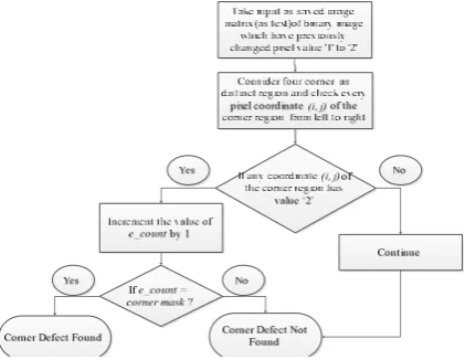
3.4.7 Algorithm to Determine Corner Defects
Let, row as the maximum number of image pixels along any row and col as the maximum number of image pixels along any column. Figure 10 shows the flow chart of corner defect detection.STEP 1. Take a variable c_count and set its value to 0. STEP 2. Check every pixel coordinates (i,j) along the range for four corner elements. If any coordinate has value ‘2’, then increment the value of c_count by 1.
STEP 3. If c_count is equal to the total corner area, then make decision that corner defect is found. Otherwise, corner defect is not found.
Fig 10: Flow chart for corner defect detection
4. EXPERIMENTAL RESULTS AND
DISCUSSION
4.1 Defect Detection
The proposed system detects surface flaw both for plain and textured tiles successfully. In this section, represents the experimental result of our proposed defect inspection technique. The defect detection rate and time efficiency are compared with the existing method [3]. We also classify here different types of defects found through defect detection process. Here it is needed to mention that during the production, many numbers of tiles are produced in industries at the same time of same colors, shape and pattern.
So, all the tiles of one shape are compared with that particular type of standard tile while processing through the computers. To get practical realization of our proposed surface flaw detection process, we have applied the proposed procedures on a sample RGB image of flat tiles. After that we check whether there is any kind of defect exists in this test image or not by applying our proposed preprocessing operations on this sample RGB image (i.e. image enhancement, noise reduction and edge detection). This is shown in the following Figure 11. In this Figure 11, we also show the reference RGB image for that test image and the output after applying preprocessing operations on it.
(a) Test Image (Flat tiles) (b) Gray Level (Flat tiles)
[image:7.595.57.275.358.548.2]
(e) Reference Image (Flat tiles) (f) Image after applying Preprocessing
Fig 11: (a) Test RGB image for flat tiles (b) Image after gray level conversion (c) Image after contrast stretching (d) Image after edge detection (e) Reference RGB image of
flat tiles (f) Image after applying preprocessing for reference image
Now consider the Figure 11(d) and Figure 11(f). The image of Figure 11(d) is found from the test RGB image after applying all the proposed preprocessing operations onto it. Then the total number of defected pixels is count in this image. Here the total number of defected pixels is 348. Again, the image of Figure 11(f) is found from the reference RGB image after applying all previous operations onto it. In this image the total number of defected pixels is 105. According to our proposed defect detection method we can say, n1=348 and n2=105. As n1 > n2, so we can make decision that defect is found in the test image.
Again, we apply the proposed detection method on a sample test RGB image for textured tiles. Like before, we have checked whether there any kinds of flaw exists in this test image or not. Then we apply our proposed preprocessing operations on this image. This is shown in the following Figure 12. In this figure, we also show the reference RGB image for that test image and the output after applying preprocessing operations on it.
(a) Test Image (Structured) (b) Image after applying Preprocessing
(c) Reference Image (Structured) (d) Image after applying Preprocessing
Fig 12: (a) Reference RGB image, (b) Final image after preprocessing for reference image, (c) Test RGB image,
(d) Final image after preprocessing for test image
Consider the Figure 12(b) and Figure 12(d). The image of Figure 12(b) is found from the test RGB image after applying all the proposed preprocessing operations onto it. Then the total number of defected pixels is count in this image. Here the total number of defected pixels is 982. Again, the image of
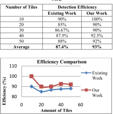
[image:8.595.318.540.230.454.2]Figure 12(d) is found from the reference RGB image after applying all previous operations onto it. In this image the total number of defected pixels is 714. According to our proposed flaw detection method we can say, n1=982 and n2=714. As n1 > n2, so we can make decision that defect is found in the test image. We have tested in total 50 ceramic tiles images for defect detection using our proposed procedures. In this case, the proposed defect detection efficiency is compared to the existing method [3]. We see that the detection rate for the proposed method is better than that of the existing method. Following Table 3 shows the efficiency comparison between the existing work and the proposed work and Figure 13 represents the detection efficiency through a chart.
Table 3. Efficiency comparison of existing work and our work
Number of Tiles Detection Efficiency Existing Work Our Work
10 90% 100%
20 85% 90%
30 86.67% 90%
40 87.5% 92.5%
50 88% 92%
[image:8.595.53.269.461.646.2]Average 87.4% 93%
Fig 13: Efficiency comparison chart between existing work and our work
We also compute the required time for the proposed method and the existing method [3]. The proposed method needs less time than the existing one. Table 4 shows the time comparison between the existing work and proposed work. Figure 14 represents time comparison through a chart.
Table 4: Time comparison between existing work and our work
Number of Tiles
Required Time (in sec.)
For Existing Method For Our Method
10 6.357379 3.538866
20 12.405698 7.558376
30 18.536334 11.145318
40 24.778622 15.150612
50 30.847008 19.242661
4.2 Defect Classification
We need to classify the various kinds of defects after defect detection. For this purpose we store the output of the above resulting image into a file as matrix form. Then previously mentioned algorithms are applied on that matrix. In the following Table 5, we show our result after applying the
80 90 100 110
0 20 40 60
E
ff
ic
ie
n
cy
(
%
)
Amount of Tiles
Efficiency Comparison
Existing Work
proposed classification algorithms for both flat and textured tiles mentioned above.
Fig 14: Time comparison between existing work
Table 5: Classification result for flat and textured tiles
Types of Defect
Result (for Flat Tiles)
Result (for Textured Tiles)
Pinhole Found Not Found
Crack Not Found
Blob Found
Spot Not Found Not Found
Edge Not Found Not Found
Corner Not Found Not Found
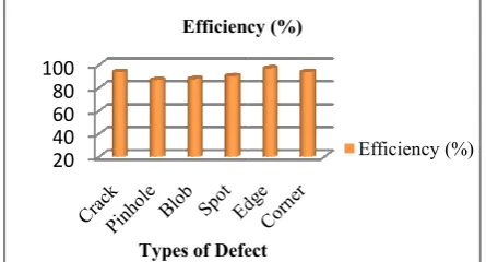
Table 6 represents the classification efficiency of the proposed method for both flat and textured tiles and
[image:9.595.56.278.104.218.2]represents this efficiency through a chart.
Table 6: Classification efficiency for proposed m
Category of Defects
Total Number of Tiles
Classification Rate for Both Flat and Textured Tiles (%) Pinhole 50 Crack Blob Spot Edge Corner
In this section, we have shown the result of the proposed defect detection method applied on a particular RGB image. We also have show the comparison between the existing method [3] and the proposed method in the case of detection efficiency and time efficiency. As a result, we find that our proposed method is better than the existing one. The detection rate of the proposed method is average 93% for a number of tiles, where for the existing method this rate is 87.4%. the proposed method requires total 19.242661 seconds to process 50 tiles, where the existing method requires 30.847008 seconds.
10 20 30 40 50
T
im
e
Number of Tiles Time Comparison
proposed classification algorithms for both flat and textured
xisting work and our
for flat and textured tiles
Result (for Textured Tiles) Not Found Found Found Not Found Not Found Not Found
represents the classification efficiency of the proposed method for both flat and textured tiles and Figure 15
Classification efficiency for proposed method
Classification Rate for Both Flat and Textured Tiles (%)
93.48 86.49 87.50 90.00 96.77 93.55
In this section, we have shown the result of the proposed defect detection method applied on a particular RGB image. We also have show the comparison between the existing method [3] and the proposed method in the case of detection As a result, we find that our proposed method is better than the existing one. The detection rate of the proposed method is average 93% for a number of tiles, where for the existing method this rate is 87.4%. Again, l 19.242661 seconds to process 50 tiles, where the existing method requires
Fig 15: Classification efficiency chart for proposed m
5. CONCLUSION AND FUTURE WORK
We have proposed a defect detection method for ceramic tiles and compared our technique with the existing defect detection method. We also have shown a comparison for defect detection and processing time between the proposed method and the existing method [3]. Detection rate of the proposed method is better than that of the existing method and we need less time to detect defects than the existing one. We also have established defect classification algorithms for different types of defects. Finally, we have calculated the performance of efficiency for defect classificatio
The proposed method fails to detect the glaze and scratch faults. However, it may be future work to detect and classify the glaze and scratch faults. We haven’t measure yet the computational time of the proposed categorization technique. In this case, future work may be calculation of the computational time and provide an efficient method of reducing computational time for defect classification.
REFERENCES
[1] R. C. Gonzalez and R. E. Woods, “
Processing”, Pearson Education (Singapore), Pte. Indian Branch, 482 F.I.E. Patparganj, 2005
[2] Puyin Liu and Hongxing Li, “ Theory and Application”. World Scientific [3] H. Elbehiery, A. Hefnawy, and M. Elewa, “
Defects Detection for Ceramic Tiles Using Image Processing and Morphological Techniques Proceedings of World Academy of Science, Engineering and Technology, vol 5, pp 158
1307-6884.
[4] C. Boukouvalas, J. Kittler, R. Marik, M. Mirmehdiand, and M. Petrou, “Ceramic Tile Inspection for
Structural Defects”, under BRITE BE5638, pp 6, University of Surrey, 2006.
[5] Se Ho Choi, Jong Pil Yun, Boyeul Seo, Young Su Park and Sang Woo Kim, “Real
Algorithm for High-Speed Steel Bar in Coil Proceedings of World Academy of Science, Engineering and Technology, Volume 21, January 2007, ISSN 1307 6884.
[6] Mohamed Roushdi, “Comparative Study of Edge Detection Algorithms Applying on the Grayscale Noisy Image Using Morphological Filter”,
Volume 6, Issue 4, December, 2006
[7] Z. Hocenski, T. Keser and A. Baumgartner
and efficient method for ceramic tile surface defect Existing Work
Our Work 20
40 60 80 100
Types of Defect Efficiency (%)
Classification efficiency chart for proposed method
5. CONCLUSION AND FUTURE WORK
We have proposed a defect detection method for ceramic tiles compared our technique with the existing defect detection method. We also have shown a comparison for defect detection and processing time between the proposed method Detection rate of the proposed the existing method and we need less time to detect defects than the existing one. We also have established defect classification algorithms for different types of defects. Finally, we have calculated the performance of efficiency for defect classification.
The proposed method fails to detect the glaze and scratch faults. However, it may be future work to detect and classify the glaze and scratch faults. We haven’t measure yet the computational time of the proposed categorization technique. future work may be calculation of the computational time and provide an efficient method of reducing computational time for defect classification.
R. E. Woods, “Digital Image ”, Pearson Education (Singapore), Pte. Ltd., Indian Branch, 482 F.I.E. Patparganj, 2005-2006.
Hongxing Li, “Fuzzy Neural Network . World Scientific, 2004.
H. Elbehiery, A. Hefnawy, and M. Elewa, “Surface Defects Detection for Ceramic Tiles Using Image Processing and Morphological Techniques”, Proceedings of World Academy of Science, Engineering and Technology, vol 5, pp 158-160, April 2005, ISSN
C. Boukouvalas, J. Kittler, R. Marik, M. Mirmehdiand, Ceramic Tile Inspection for Colour and ”, under BRITE-EURAM, project no. BE5638, pp 6, University of Surrey, 2006.
Se Ho Choi, Jong Pil Yun, Boyeul Seo, Young Su Park Real-Time Defects Detection Speed Steel Bar in Coil”, dings of World Academy of Science, Engineering and Technology, Volume 21, January 2007, ISSN
1307-“Comparative Study of Edge Detection Algorithms Applying on the Grayscale Noisy Image Using Morphological Filter”, GVIP Journal,
6, Issue 4, December, 2006.
Z. Hocenski, T. Keser and A. Baumgartner, “A simple and efficient method for ceramic tile surface defect
Types of Defect Efficiency (%)
[image:9.595.54.283.423.530.2]detection”, IEEE International Symposium on Industrial Electronics (ISIE2007), Pp. 1606-1611, 4-7 June 2007.
[8] G. S. Desoli, S. Fiornvanti, R. Fioravanti and D. Corso, “A System for Automated Visual Inspection of Ceramic Tiles”, Dept. of Biophysical and Electronic Engineering, Via Opera Pia 11/A 16145 Genova, University of Genoa, Italy.
[9] F. S. Najafabadi, H. Pourghassem, “Corner Defect Detection Based on Dot Product in Ceramic Tile Images”, IEEE 7th International Colloquium on Signal Processing and its Applications, 2011.