An Efficient Design of 3bit and 4bit Flash ADC
Arunkumar P Chavan
Rekha G
P Narashimaraja
Department of Electronics and Communication, R V college of Engineering, Bangalore 560059, India.
ABSTRACT
The performance of Flash Analog-to-Digital converter is greatly influenced by the choice of Comparator and Thermometer-to- Binary encoder design. The work describes the design and pre-simulation of a , 3bit and an 4bit analog to digital converter for low power CMOS. It requires 2N-1 comparators, an encoder to convert thermometer code to binary code. The design is simulated in cadence environment using spectre simulator under 90nm technology. The pre simulation results for the design shows a low power dissipation of 87uw for the comparator and 1.05mW and 1.984mW power dissipation for 3-bit and 4-bit Flash ADC respectively. The circuit operates with an input frequency of 25MHz and 1.5V supply with a conversion time of 2.162ns and 6.182ns for 3-bit and 4-bit ADC respectively.
Keywords
Low-power, CMOS comparator, Flash ADC, Thermometer encoder.
1.
INTRODUCTION
An analog-to-digital converter (ADC) is a device that converts the input continuous physical quantity to a digital number that represents the quantity's amplitude. The result is a sequence of digital values that have converted a continuous-time and continuous-amplitude analog signal to a discrete-time and discrete-amplitude digital signal. A direct-conversion ADC or flash ADC has a bank of comparators sampling the input signal in parallel, each firing for their decoded voltage range. The comparator bank feeds an encoder logic circuit that generates a code for each voltage range.
2.
FLASH CONVERTER
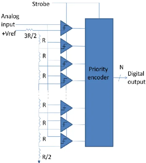
Flash ADCs (sometimes called parallel ADCs) are the fastest type of ADC and use large numbers of comparators. The input signal is applied to all the comparators at once, so the thermometer output is delayed by only one comparator delay from the input, and the encoder N-bit output by only a few gate delays on top of that, so the process is very fast. An N-bit flash ADC consists of 2N resistors and 2N–1 comparators arranged as in Figure Fig 1. Each comparator has a reference voltage which is 1 LSB higher than that of the one below it in the chain. For a given input voltage, all the comparators below a certain point will have their input voltage larger than their reference voltage and a “1” logic output, and all the comparators above that point will have a reference voltage larger than the input voltage and a “0” logic output. The 2N–1
[image:1.595.320.558.192.459.2]comparator outputs therefore behave in a way analogous to a mercury thermometer, and the output code at this point is sometimes called a thermometer code. Since 2N–1 data outputs are not really practical, they are processed by a decoder to generate an N-bit binary output.
Figure 1: N-Bit Flash ADC
The architecture uses large numbers of resistors and comparators and is limited to low resolutions, and if it is to be fast, each comparator must run at relatively high power levels. Hence, the problems of flash ADCs include limited resolution, high power dissipation because of the large number of high speed comparators and relatively large (and therefore expensive) chip sizes. In addition, the resistance of the reference resistor chain must be kept low to supply adequate bias current to the fast comparators.
2.1
Comparator
Fig 2: Preamplifier-Latch comparator
The preamplifier stage improves the sensitivity of the comparator and isolates the comparator input from switching noise of the positive feedback stage [3]. The latch stage gives the information about which of the input signals is larger and amplifies the difference between the signals [7].
2.2
Thermometer to Binary code converter
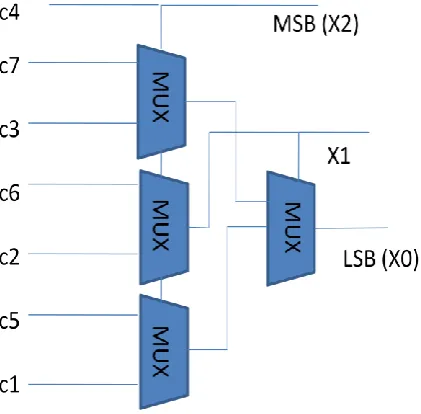
[image:2.595.59.285.74.267.2]The logic encoder used for 3bit and 4bit ADC are as shown in fig 3 and fig 4. This is a multiplexer based encoder which converts thermometer codes to binary codes. Table 1 and table 2 show the truth table for 3bit and 4bit encoders. The multiplexers used are designed using transmission gates for better accuracy.
Fig 3: Logic Encoder for 3bit ADC
[image:2.595.319.545.89.487.2]Table 1: Truth table for 3bit encoder
Fig 4: Logic Encoder for 4bit ADC
[image:2.595.62.273.453.660.2]3.
PRE SIMULATION RESULTS
3.1
Comparator output
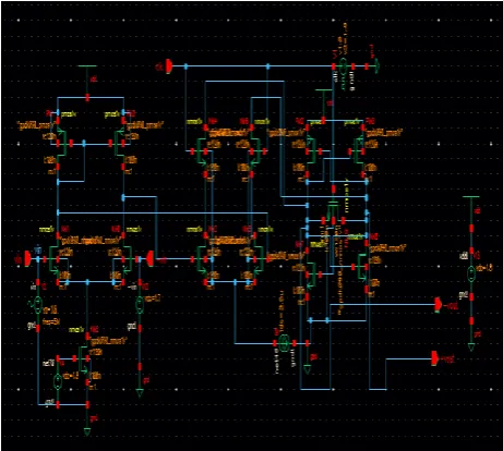
[image:3.595.317.562.74.247.2]The schematic of comparator using 90nm technology is shown in fig 4. The input signal applied to the non-inverting terminal is a sine wave and a dc reference voltage is applied to the inverting terminal of the comparator. The resulting waveform at the output of the comparator is as shown in fig 5.
[image:3.595.55.286.163.370.2]Fig 5: Schematic of comparator
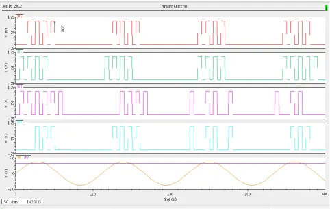
Fig 6: Comparator output waveform
3.2 Flash ADC output
The above obtained 2N-1 comparator outputs are encoded into 3bit output and 4bit output for 3bit and 4bit ADCs respectively using an encoder and the resulting waveform of both resolution ADCs are as shown in fig 9 and fig 10. The schematic views of ADCs are shown in fig 7 and fig 8.
[image:3.595.317.560.277.478.2]Fig 7: Schematic view of 3bit ADC
Fig 8: Schematic view of 4bit ADC
[image:3.595.55.291.387.591.2] [image:3.595.317.542.496.692.2]Fig 10: Output waveform of 4bit ADC
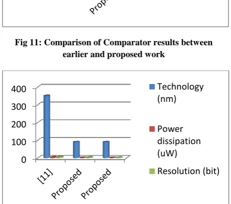
[image:4.595.55.542.600.708.2]Table 3: Comparison of Present work with earlier works for comparator
Table 4: Comparison of Present work with earlier works for ADC
Table 3 and Table 4 shows the parameter values obtained for the comparator and 4bit ADC circuit under 90nm technology with supply voltage equal to 1.5V.
References Technology Power dissipation Voltage
[4]
[5]
[6]
Proposed work
350nm
250nm
180nm
90nm
200uW
153uW
132.7uW
87uW
2V
1.8V
2V
1.5V
References Technology Resolution Power dissipation Voltage
[11]
Proposed work
Proposed work
350nm
90nm
90nm
6-bit 3-bit
4-bit
4.36mW
1.05mW
1.984mW
3.3V
1.5V
Fig 11: Comparison of Comparator results between earlier and proposed work
Fig 12: Comparison of ADC results between earlier and proposed work
Comparison between earlier work and proposed work for comparator and ADC results are shown in Fig 11 and Fig 12.
4 CONCLUSIONS
The problem of flash ADCs lies with limited resolution, high power dissipation because of the large number of high speed comparator. In this regard an attempt is made to design low-power 3bit and 4bit ADCs. The design and Pre simulation are carried out in cadence environment using spectre simulator under 90nm technology. The pre simulation results for the design shows a low power dissipation of 87uw for the comparator and 1.05mW and 1.984mW power dissipation for 3-bit and 4-bit Flash ADC respectively. The circuit operates with an input frequency of 25MHz and 1.5V supply with a conversion time of 2.162ns and 6.182ns for 3-bit and 4-bit ADC respectively. The ADC design can be used for low power and high speed applications. The proposed architecture can be extended to higher resolution. For the proposed architecture area optimization must be done in the future.
REFERENCES
[1] Shubhara Yewale, Radheshyam Gamad “Design of Low Power and High SpeedMOS Comparator for A/D [2] Converter application”, Wireless Engineering and
Technology, 2012, 3, 90-95.
[3] B. Razavi, “Deign of Analog CMOS Integrated Circuits,” Tata McGraw-Hill, Delhi, 2002.
[4] R. Wang, K. Li, J. Zhang and B. Nie, “A High Speed High Resolution Latch Comparator For-Pipeline ADC,”
IEEE International Workshop on Anti-counterfeiting, Se- curity, Identification, Xiamen, 16-18 April 2007, pp. 28- 31.
[5] Y. Degerli, N. Fourches, M. Rouger and P. Lut, “Low Power Autozeroed High-Speed Comparator for the Read- out Chain of a CMOS Monolithic Active Pixel Sensor Based Vertex Detector,” IEEE Transactions on Nuclear Science, Vol. 50, No. 5, 2003, pp. 1-21.
[6] Y. Sun, Y. S. Wang and F. C. Lai, “Low Power High Speed Switched Current Comparator,” IEEE 14th Inter- national Conference, Ciechocinek, 21-23 June 2007, pp. 305-308.
[7] M. Panchore and R. S. Gamad, “Low Power and High Speed CMOS Comparator Design Using 0.18 μm Tech- nology,” International Journal of Electronic Engineering Research, Research India Publications, Vol. 2, No. 1, 2010, pp. 71-77.
[8] W. Rong, W. Xiaobo and Y. Xiaolang, “A Dynamic CMOS Comparator with High Precision and Resolution,” IEEE Proceedings of 7th International Conference on So- lid-State and Integrated Circuits Technology, 18-21 Oc- tober 2004, pp. 1567-1570.
[9] ShaileshRadhakrishnan, Mingzhen Wang, Chien-In Henry Chen,“Low-Power 4-b 2.5GSPS Pipelined Flash Analog-to-Digital Converters in 3um CMOS”, IEEE Instrumentation and Measurement Technology Conference, vol. 1, pp. 287 – 292, May. 2005.
[10]Chia-Nan Yeh and Yen-Tai Lai, “A Novel Flash Analog-to-Digital Converter”, IEEE J, 2008.
[11]G. M. Yin, F. Op’tEynde, and W. Sansen, “A high-speed CMOS comparator with 8bit resolution”, IEEE J. Solid -State Circuits, vol. 27, 1992.
[12]A.V. Bapat, Dr. A. S. Gandhi, Dr. A. M. Dighe, “CMOS Implementation of Serial Flash Analog to Digital Converter”, International Conference on VLSI, Communication & Instrumentation (ICVCI) 2011
AUTHORS PROFILE
A. Arunkumar. P Chavan born on July, 4th, 1987 in Karnataka, India, obtained his B.E degree in Electronics and Communication Engineering from Visvesvaraya Technological University (VTU), Belgaum, India. Currently pursuing M.Tech in VLSI Design and Embedded Systems. His areas of interest are VLSI design, Analog circuit design and digital electronics.
B. Rekha G born on March, 15th, 1990 in Karnataka, India, obtained her B.E degree in Electronics and Communication Engineering from Visvesvaraya Technological University (VTU), Belgaum, India. Currently pursuing M.Tech in VLSI Design and Embedded Systems. Her areas of interest are VLSI design, Image Processing, and Digital electronics.
C. Narashimaraja. P born on January, 31st, 1982 in Tamilnadu, India, obtained his BE degree in Electronics from Madurai Kamaraj university, in 2004 and ME degree in VLSI Design from Bharath institute of higher education & research, in 2006. Currently, Is an Assistant professor at RV College of Engineering. His research interest are in the field of VLSI architectures, Memory design and Analog design.
0 100 200 300 400 Technology(n m) Power dissipation (uW) 0 100 200 300
400 Technology
(nm)
Power dissipation (uW)