R E S E A R C H
Open Access
An optimized two-level discrete wavelet
implementation using residue number system
Husam Y. Alzaq
*and B. Berk Ustundag
Abstract
Using discrete wavelet transform (DWT) in high-speed signal processing applications imposes a high degree of caution to hardware resource availability, latency and power consumption. In this paper, we investigated the design and implementation aspects of a multiplier-free two-level DWT by using residue number system (RNS). The proposed two-level takes the advantage of performing the multiplication operations using only the memory without involving special multiplier units, which preserves valuable resources for other critical tasks within the FPGA. The design was implemented and synthesized in ZYNQ ZC706 development kit, taking advantage of embedded block RAMs (BRAMs). The results of the overall experimentations showed that there is a considerable improve in the proposed two-level DWT design with regard to latency and peak signal-to-noise ratio (PSNR) precision value in the final output.
Keywords: Discrete wavelet transform (DWT), Digital signal processing (DSP), Residue number system (RNS), Field programmable gate array (FPGA)
1 Introduction
Discrete wavelet transform (DWT) [1–5] is a linear sig-nal processing technique that transforms a time domain
signal to “wavelet” domain [6]. DWT is usually
imple-mented using the finite impulse response (FIR) filter bank structures [7]. Figure 1shows a convolution-based five-tap FIR filter with five multipliers, known as
multiplier-accumulator (MAC) structure. In Fig. 1, the multipliers
are involved in multiplying an inputx[n] with filter coef-ficients,bi. The direct implementation of theN-tap filter
requiresN multipliers, which are an expensive resource
in field-programmable gate array (FPGA). With regard to this fact, it is known and clear that convolution-based method requires massive computations, takes more phys-ical space, and consumes more power [8]; hence,
lifting-based (LS) [9] has been developed and implemented to
improve these limitation.
In this work, we preferred the conventional convolution-based DWT implementation over the LS for the following reasons. In LS, as the critical path delay (CPD) increases, the energy per operation increases and the operating frequency decreases [10]. In [11, 12], the authors found
*Correspondence:[email protected]
Department of Computer Engineering, Faculty of Computer Engineering, Istanbul Technical University, Maslak, Ayazaga, 34469 Istanbul, Turkey
out that as the length of the filter (N) increases, the
CPD is increased, respectively. Hence, the sequence of multiplication and addition will be longer than the convolution-based scheme. Therefore, LS is observed to have poor scalability and is inappropriate for large filter lengths [13,14]. In addition, LS requires temporary registers to store the intermediate results, which takes up more storage area and as well consumes more power [15,16]. For these reasons, we decided to implement the DWT using the convolution-based approach, but with multiplierless architecture.
Multiplierless approaches eliminate the use of multipli-ers by replacing individual coefficient multiplimultipli-ers with a single multiplier block, known as a multiple constant mul-tiplication (MCM). Because filter coefficients are fixed and determined in advanced, the multiplication of filter coefficients by an input leads to area, delay, and power-efficient architectures [17].
The existing multiplierless algorithms can be divided into two general classes: they either reduce the number of multipliers or totally replace them with a simplified circuit logic. The most popular reduction algorithms are
graph-based eliminations (GE) [18] and common subexpression
elimination (CSE) techniques [19–21]. The drawback of
CSE algorithms is that its performance depends on the representations of the coefficients and also limited by the
Fig. 1Five-tap finite impulse response filter
constant bit widths [20], whereas the GE require more
computational resources due to a larger search space [22]. On the other hand, several multiplierless architectures that eliminate all multipliers have been proposed. Dis-tributed arithmetic (DA) efficiently performs the inner product function in a bit-serial manner via a look-up table (LUT) scheme, followed by shift accumulation operations [23–25]. Based on our previous experience, we identified that the ROM size in DA-based structures increases with the increase in the word length [26]. Residue number sys-tem (RNS) is a highly parallel non-weighted arithmetic system that is based on the residue of division opera-tion of integers using the look-up table (LUT) scheme
[27–29]. The key advantage of RNS is gained by
reduc-ing an arithmetic operation to a set of concurrent, but simple, operations. Another advantage of RNS is its large dynamic range, which is divided into independent smaller ranges, where addition and multiplication operations are performed in parallel without a carry propagation among them. Several applications, such as digital filters, benefit from the RNS implementation, e.g., [30–32]. To the best of our knowledge, the aforementioned approaches consider only one-level DWT implementation.
1.1 Contribution of this paper
This article focuses exclusively on the implementation of two-level multiplier-free DWT. We propose a new design of two-level RNS-based DWT that efficiently uses the memory elements in the first-level DWT and do not employ any memory element in the next levels. In addi-tion, this design eliminates the use of multiple residue-to-binary converters (RBCs) between consecutive levels. Generally, the number of level is bounded by the output
word length and we determine it mathematically (Eqs.15
and16). Finally, the proposed RNS-based approach could
achieve high PSNR values with simple hardware structure and consume less power.
The remainder of this paper is organized as follows:
In Section 2, the theoretical background on RNS is
given. Section3illustrates the implementation of discrete wavelet transform. The implementation of the proposed two-level RNS is also presented. We further show an
ana-lytical comparison between these approaches. Section 4
presents the performance results. Finally, conclusions are drawn in Section5.
2 Preliminaries
2.1 Discrete wavelet transform
The wavelet decomposition mainly depends on the
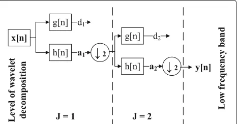
orthonormal filter banks. Figure2 shows a two-channel
wavelet structure for decomposition, where x[n] is the
input signal,g[n] is the high-pass filter,h[n] is the low-pass filter, and↓2 is the down-sampling by a factor of two. By this way, each filter creates a series of coefficients that represent and compact the original signal information.
Mathematically, a signaly[n] consists of high and low-frequency components, as shown in Eq. (1). It shows that the obtained signal can be represented by using half the coefficients, because they are decimated by 2.
y[n]=yhigh[n−1]+ylow[n−1] (1)
The decimated low-pass filtered output is recursively passed through identical filter banks in order to add the dimension of varying resolution at every stage. Equations (2) and (3) mathematically express the filtering process of a signal through a digital high-pass filterg[k] and low-pass filterh[k]. This operation corresponds to a convolution with an impulse response ofk-tap filters.
yhigh[n]=
k
g[k] .x[2n−k] (2)
ylow[n]=
k
h[k] .x[2n−k] (3)
where n becomes 2n, representing the down-sampling
process. The output ylow[n] provides an approximation
signal, while yhigh[n] provides the detailed signal. There
have been several wavelet filters proposed in litera-ture, but in this paper, we have restricted ourselves to
Daubechies wavelet filters only [33]. Because the
down-sampling process follows each filter (as shown in Fig.2), Eq. (3) can be rewritten without the decimation factor as:
y[n]=
N−1
k=0
h[k] .x[n−k] (4)
whereNis the number filter tap. For the sake of simplicity of representing Eq. (4),x[n−k] is replaced byx[k].
2.2 Residue number system (RNS)
RNS [27, 28] is a non-weighted number system that
performs parallel carry-free addition and multiplication arithmetic. In DSP applications, which require intensive computations, the carry-free propagation allows for con-current computation in each residue channel.
Another aspect of using RNS is that an integer, within a large dynamic range, can be uniquely represented by set of residues,P, that are of much smaller values, corresponding to the size of the moduli set.
The RNS moduli set,P = m1,m2,. . .,mq, consists of qchannels. Eachmirepresents a positive relatively prime
integer, that is GCD(mi,mj)=1, fori=j.1Any number, X∈ZM =0, 1,. . .M−1, is uniquely represented in RNS
by its residues|X|mi, which is the remainder of divisionX
bymiandMis defined in Eq. (5),
M=qi=1mi=m1∗m2∗ · · · ∗mq (5)
M determines the range of unsigned numbers in
[0,M−1]. In particular, M should be greater than the
largest expected output.
In the RNS representation, addition and multiplication are performed entirely in parallel on each modulo,
Z=X◦Y −→RNS Zmi= |Xmi◦Ymi|mi (6)
where◦represents the addition, subtraction, or multipli-cation operation; andmi∈P.
Mapping from the RNS system to integers,Z, is
per-formed by Chinese reminder theorem (CRT) [34–36]. The
CRT states that binary/decimal representation of a
num-ber can be obtained from its RNS through Eq. (7),
pro-vided all elements of the moduli set are pairwise relatively prime.
The implementation of RNS-based DWT is obtained by substituting Eq. (6) into (4)
implemented byqFIR filters that are working in parallel.
For designing an efficient RNS-based DWT, the choice of the moduli set and hardware design of residue-to-binary conversion are two critical issues that should be considered. Most widely studied moduli sets are given as a power of two due to the attractive arith-metic properties of these modulo sets. For example,
{2n − 1, 2n, 2n+1 − 1} [37] {2n − 1, 2n, 2n + 1} [38]
and {2n, 22n − 1, 22n + 1} [39] have been investigated. A four-moduli set has been suggested to increase the dynamic range, e.g.,{2n−1, 2n, 2n+1, 2n+1−1}[40] and
{2n−1, 2n, 2n+1, 22n+1}[41].
In this work, the moduli setPn= {2n−1, 2n, 2n+1−1}
is used for three reasons. First reason being that the
mod-ular adder is simple and identical for bothm1 = 2n−1
and m3 = 2n+1 − 1. Secondly, for small n = 7, the
dynamic range ofP7is large andMis equal to 4145280,
which would efficiently express real numbers in the range [−2.5, 2.5] using 16-bit fixed-point representation, pro-vided scaling and rounding are done properly. We assume that this interval is sufficient to map the input values, which does not exceeds±2. Thirdly, the reverse converter unit is simple and regular [36] because it does not employ any memory.
3 DWT implementation methodology
As mentioned in the previous sections, the wavelet trans-form of a signal can be pertrans-formed by FIR filters, where the convolution operations are achieved by multiplying an input signal by the wavelet coefficients. In contrast, RNS-based approach has replaced the multiplication units with a suitable memory to perform the multiplication operations.
3.1 DWT implementation using RNS
Figure 3 shows the steps that are involved in
RNS-based DWT approach. These steps are divided into offline and online steps. The offline steps are per-formed by converting the filter coefficients to RNS numbers and storing the result in a LUT. The online steps are used in converting each input values into RNS-system, before performing the filtering opera-tions. Finally, the produced result is converted back to real-number system. We explained these process in Section3.1.1.
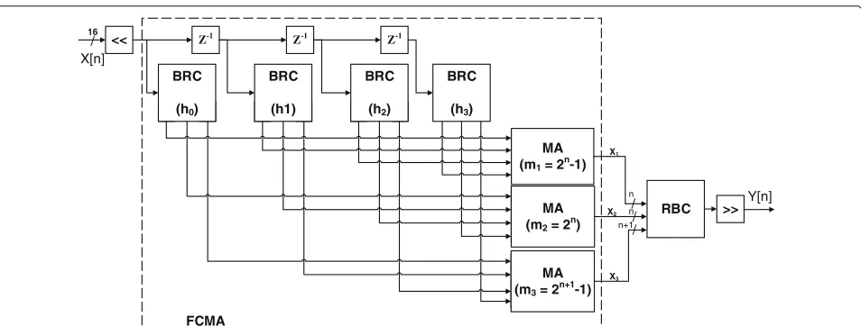
In general, the implementation of RNS-based DWT has essentially three components— i.e., the modulo adders (MA), forward and reverse converter. The forward con-verter, also known as binary-to-residue converter (BRC), is used to convert a binary input number to residue num-bers. In contrast, the reverse converter, also known as residue-to-binary converter (RBC), is used to obtain the result in a binary format from the residue numbers. These
components are shown in Fig. 4. We will refer to the
forward-Fig. 3The RNS-based DWT offline and online steps to perform the filtering operations. The offline steps are performed one time, while the online are performed for each input.qis the number of channels
converter and modular-adders (FCMA), shown inside the dashed-line box in Fig.4.
3.1.1 Binary-to-residue converter (BRC)
The BRC is used to convert the result of multiplying an
input number by a wavelet coefficient toqresidue
num-bers by using LUT, shift, and modulo adders, where q
is the number of channels. This procedure ensures that the multiplication operation is performed by using only memory.
RNS-system number conversion The received input and wavelet coefficients span the real number and might take small values. One of the main limitation of using RNS-number representation is that it only operates with
positive integer numbers from [0,M−1]. The DWT
coefficients are generally close to zero and between
−1 and 1. Therefore, it is important to cope with
both negative numbers and small numbers. To han-dle negative numbers, we mapped the real number to RNS range. Assuming the input samples are in
[−2.5, 2.5], we mapped any value in this range to a
unique value in [0,(M−1)]. Any sample, which does
not fit this interval, will produce incorrect values. Hence, the interval should be large enough to map all the numbers.
In principle, the received sampleX[i] is shiftedy posi-tions to the left (multiplying by 2y, step 4 in Fig.3). This
step ensures that X[i] is a y-bit fixed point integer. In a similar manner, the wavelet coefficients are scaled by shifting itzpositions to the left (step 1 in Fig.3). In our
design, we set the filter scaling factor z to 11 and as a
result, the coefficients of DB2 (Eq.9) are multiplied by 211
>>
<< Z-1 Z-1 Z-1
BRC
(h0)
BRC
(h3) BRC
(h2) BRC
(h1)
MA (m2= 2n)
MA (m3= 2n+1-1)
MA (m1= 2n-1)
RBC
/ /
n
n+1
/
n 16
/
FCMA
X[n]
Y[n]
X1
X3
X2
and rewritten as shown in Eq.9.
ylow[n]= −266x[n]+459x[n−1]
+1713x[n−2]+989x[n−3] (9)
Modulomimultiplier The multiplication of the received
sample by the filter coefficients, which are constants, can be performed via indexing the LUT. It is critical to iden-tify the size of LUT because as the word length,w, of the received sample is increased, the memory size becomes 2w. Additionally, the design requireqLUTs to perform the modulo multiplication.
We suggested several techniques to overcome these inadequate requirements. Instead of preserving a
dedi-cated memory for each modulo mi, one memory that
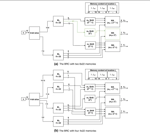
contains all module results is used. In this scheme, each word at locationjcontainsqmodules ofhk∗j∗211. Figure5
shows the internal BRC block design of the three-channel
moduli setP7 = {127, 128, 255}with its memory-map at
the right top corner. This shows that, for a locationj, the least significant 8-bit contains|hk ∗x|m3, the next 7-bit contains|hk∗x|m2and the most significant 7−bit contains
|hk∗x|m1, which can be generalized as shown in Eq. (10) (steps 2 and 3 from Fig.3). The advantage of this method is
x 16/ Memory content at location j
/
7
The BRC with two 8x22 memories
x 16/ Memory content at location j
/
7
The BRC with four 4x22 memories
(a)
(b)
Fig. 5The block diagram of the binary-to-residue converter for the three-channel RNS-based DWT,P7= {127, 128, 255}(a) with two, (b) with four
identical memories. The green blocks are not required because the shift result is always zero form2. The memory content at locationjis as shown in
that no extra hardware is required to separate each mod-ule value. Table1shows the memory contents ofh1in RNS
system using 4×22 LUT.
It is obvious that if the input word length is 16 bits, then
the LUT size becomes huge because 216 locations will
be needed. One way to reduce the size of memory is
to divide it into smaller size, each consisting of 2 ×22
bits or 4×22 bits. Figure5shows the block diagram of
the binary-to-residue converter with two and four mem-ories, respectively. However, the output of each memory should be combined, so that the final result is correct. It is worth noting that this division comes with a cost in terms of additional adders and registers are used (discussed in Section3.4).
According to the previous improvements, the
RNS-based system works as follows (step 5 from Fig.3).
Sup-pose that four memories are used, each of 16 locations. The inputX16−bit = (x1,x2,x3,x4) will be divided into
four segments. Each 4-bit segment will be fed into one memory, so that the 22-bit can be found, which will then
be divided into three outputs, corresponding to |hk ∗
xl ∗211|mi. We want to emphasize that this result is the
multiplication of each 4-bit with a filter coefficient with respect tomi.
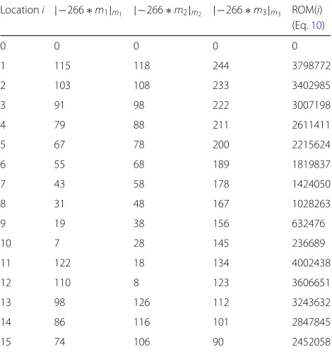
Table 1The memory content ofh0 = −0.1294 or 757(−266)
multiplied by 211inP
7= {127, 128, 255}when word length is 4 Locationi |−266∗m1|m1 |−266∗m2|m2 |−266∗m3|m3 ROM(i) (Eq.10)
0 0 0 0 0
1 115 118 244 3798772
2 103 108 233 3402985
3 91 98 222 3007198
4 79 88 211 2611411
5 67 78 200 2215624
6 55 68 189 1819837
7 43 58 178 1424050
8 31 48 167 1028263
9 19 38 156 632476
10 7 28 145 236689
11 122 18 134 4002438
12 110 8 123 3606651
13 98 126 112 3243632
14 86 116 101 2847845
15 74 106 90 2452058
To obtain the final multiplication’s result, eachmi
out-put will be shifted byl positions, wherelis the index of the lowest input bit (4, 8, or 12). The modular multiplica-tion and shift for 2n−1 and 2n+1−1 can be achieved by a left circular shift (left rotate) forlpositions, whereas the modular multiplication and shift for 2ncan be achieved by a left shift forlpositions [37]. Finally, the modulo adder adds the corresponding output.
3.1.2 Modulo adder (MA)
The modulo adders are required for adding the results from a modular multiplier as well as for the reverse con-verter. In this work, two types of MAs are necessary—i.e.,
the first one is based on 2n and the other is based on
2n−1. Modulo 2nadder is just the lowestnbits of adding two integer numbers, where the carry is ignored. Modulo 2n−1 adder differs from modulo 2nadder in that the carry should be considered to limit the result to not be greater than 2n−1, as in Eq. (11).
|x+y|2n−1=
x+y ifx+y2n−1,
x+y+1 otherwise (11)
To improve the design and enhance the speed, a
parallel-prefix carry computational structure is used [42–44],
which allows the implementation of highly efficient com-binational and pipelined circuits for modular arithmetic.
3.1.3 The reverse converter
The Chinese remainder theorem (CRT) [34] provides the
theoretical basis for converting a residue number into a natural integer. The direct implementation of the CRT is inefficient because it requires a divider unit and several multipliers to determine the final output. However, the moduli setPn = {2n−1, 2n, 2n+1−1}can be efficiently
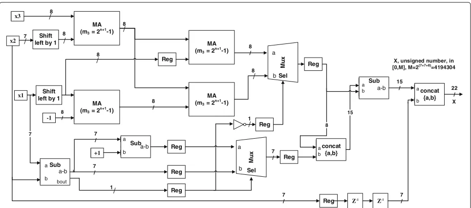
implemented by four modulo adders and two multiplexers (step 6 from Fig. 3) [36]. Figure 6 shows the block
dia-gram of the RBC ofP7, which is adapted from [36]. The
output of the RBC is unsigned(3∗n+1)-bit integer num-ber. The actual signed number can be found by shifting the resulty+zpositions to the left, which is equivalent to dividing by 2y+z.yandzare the scaled values of the input and wavelet coefficients, respectively. Generally, the word
length of one-level DWT is bounded by Eq.12and should
not exceed 3∗n−2 bits. Subtracting 3 is required because 2.5 is added to the input samples in order to have a 3-bit unsigned integer.
3∗n+1≥y+z+3 (12)
3.2 Example
Mu
X, unsigned number, in [0,M], M=2(7+7+8)
=4194304
X
Fig. 6The block diagram of the pipelined residue-to-binary converter for the three-channel RNS-based DWT,P7= {127, 128, 255}. Four identical
2n+1−1 MAs, three subtractors and two multiplexers are generally required for RBC. Two shift registers are used for extending the 7-bit input by
one bit. In the real implementation this operation does not add any cost because this operation is just equivalent to appending 0 at the first location of the input signal
can be rewritten as(0000 0010 0001 1010)2 orx1 = 0,
x2 = 2,x3 = 1 and x4 = 10. These values are used
to index the memory and the value of multiplyingxi by
h0can be found in Table1—i.e., 0, 3402985, 3798772
and 236689, respectively. From the table, the correspond-ing module of x1 is (0, 0, 0)P7, x2 is (103, 108, 233)P7,
x3 is(115, 118, 244)P7 and the corresponding module of
x4 is (7, 28, 145)P7. After that, the value of h0 ∗x2 is
shifted eight-position corresponding tomiand the value
of h0∗x3 is shifted four-position corresponding tomi.
For the case of x3, the mid value is shifted 8 bit to the
left, whereas the other values is circular shifted by 8 bit to the left and the result becomes (79, 0, 233)P7. It is worth noting that the mid value is always 0 because the word width is 7 and is less than the shift value, 8. For the case of x2, the mid value is shifted 4 bit to the left, whereas the other values is circular shifted for four positions and the result becomes(62, 96, 79)P7. The sum of the partial results, performed via tree of two-input MAs, is (148, 124, 457)P7 or (21, 124, 202)P7, which is equivalent to(mod(−143108, 127), mod(−143108, 128), mod(−143108, 255)), respectively. Finally, the output of this memory-based multiplication is aggregated with next filter-taps using MAs.
3.3 Two-level DWT implementation
The two-level discrete wavelet transform comprises of two cascaded one-level DWTs (in series), where the output of the first level is fed into the second level (as shown in Fig.2). Figure7ashows the design of two-level RNS-based DWT, which involves two identical FCMA
and two RBC blocks. The FCMA block is the RNS-based filtering (multiplication) block. It is obvious that convert-ing between the number systems back and forth intro-duces some latency. Latency is defined as the number of clock cycles required to generate the first output sam-ple once the input signal is applied. The latency,τ, of the two-level design is given by
τ =2∗(τFCMA+τRBC) (13)
whereτFCMA is the RNS-based filter latency andτRBC is
the RNS-to-binary converting delay, respectively.
In this work, we suggest to eliminate the first RBC and feed the output of the first FCMA block into the second
block, as shown in Fig.7b. The advantage of this
elimi-nation is that the final output will be solely computed by one RBC component and one shift register. As a result, the latency becomes:
τ =2∗τFCMA+τRBC (14)
The only restriction is that the range of the used moduli-set should be greater than the maximum expected value,
tho, which can be computed as follows:
tho=
andzare the input and filter scaling factors, respectively;
conse-<< 6 RBC >> 28 RBC
FCMA FCMA RBC
FCMA (L2) FCMA
>> 19
<< 8 >> 11
2-level RNS-based design, (n=10)
The proposed 2-level RNS-based Design, (n=10)
X X
Y
Y
(a)
(b)
Fig. 7The block diagram of two-level RNS-based DWT design (a), the full design with two RBCs, and (b) the proposed design, which eliminates the middle RBC to improve the latency. FCMA represents FIR filtering process in RNS
quence, the word length of two-level DWT is bounded by Eq.16and should not exceed 3∗n−2 bits.
3∗n+1≥y+(2∗z)+3 (16)
where(3∗n+1)is the moduli-set word length. Eventually, Eq.16can be generalized to any DWT level,(l), by using the following inequality:
3∗n−2≥y+(l∗z) (17)
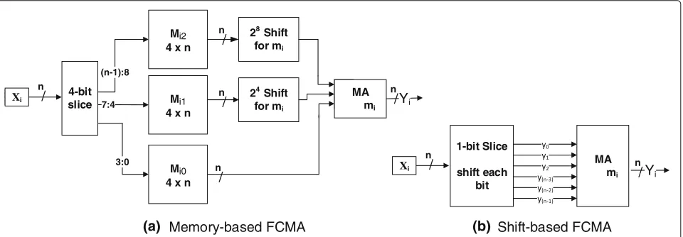
3.3.1 The design of the second FCMA
The FCMA of the proposed stage can be implemented by two different techniques. The first one is based on mem-ory that stores the multiplication result of multiplying an integer by the filter coefficient (Fig. 8a) and the second one is based on shift-add operations of the input by 2r, whereris the position of each “1” of the filter coefficient (Fig.8b). For example, from Table1,h0is equal to 757 or (01011110101)2, which is required to (circular) shift the
input by 0, 2, 4, 5, 6, 7, 9 and adding them to find the final multiplication result. The key feature of this technique is that each multiplication operation is a left (circular) shift,
which can be implemented by rewiring the order of the input bits. Indeed, the implementation is simple, and does not require any special circuits except several MAs to sum up the result. In the following sections, we refer to the optimized FCMA as memory-based, if it employs memory elements or shift-based, if it does not employ any memory.
3.4 Hardware complexity
3.4.1 Memory usage
RNS techniques employs memory elements as a key resource to avoid multiplying two input variables. As the number of level increases, the number of memory ele-ments changes. Assuming that the length of the received
word isw−bit and there areN filter-tap, we define the
size of a memory element bya×b, whereaandbare the
word size of input and output, respectively. The value ofa
determines the size of the memory, 2a. The total number
of memory elements that is occupied by an RNS-based filter is N ∗ w/aof (a×b). This Eq. shows that the number of memory elements increases linearly with the
number of filter taps (as shown in Fig. 8a), while the
3:0
Y
(n-1):8
7:4
28Shift for mi
4-bit slice
Mi2
4 x n
Mi1
4 x n
Mi0
4 x n
24Shift for mi
/
n
/
n
/
n
/
n
Memory-based FCMA
MA mi
Y Xi /
n 1-bit Slice
shift each bit
/
n
Shift-based FCMA
MA mi
Xi /
n
(a) (b)
memory size remains constant(a×b), but increased asa
andbincrease. The only overhead with largeais that the number of MA, which are required to sum up the final
result, is increased. Table 2 shows a comparison of the
memory usage whenw=16.
If the FCMA at the second stage is implemented by means of memory (memory-based FCMA), then the num-ber of required memory can be calculated as follows:
q∗N∗ n a
(18)
For instance, a three-channel ofP10FCMA has 6
memo-ries of(4×10)and 3 memories of (4×11). Therefore, the FCMA at the second stage requires 36 memory elements and in total 52 are required for the whole design.
The design of FCMA at the second stage can be improved by eliminating all the memory at FCMA, as
shown in Fig. 8b. In this case, the proposed shift-based
FCMA performs the multiplying operations via shift oations and MA units. The shift operation is always
per-formed via rewiring the bits [37], which has no cost in
terms of delay and hardware.
3.4.2 Adder counts
In addition to the memory complexity, we could derive an expression for the overall adder counts. In the following analysis, we can neglect the difference between(2n−1) and(2n+1−1) MAs because it will not affect the total number of MAs.
For a word length w and N-tap filter, the q-channel
FCMA implementation requires N BRC blocks and
(q∗(N−1))two-input MA blocks to compute the final
result (Fig.4). Each BRC requires at most(q∗(w/a−1))
two-input MA blocks (Fig.5). Likewise, the RBC has four
MA blocks, three subtractors, and two multiplexers. Thus, the total number of MA blocks at one-level RNS-based is given by:
MAt=q∗N∗(w/a−1)+q∗(N−1)+4
=q∗N∗w/a−qN+qN−q+4
=q∗(N∗w/a−1)+4
(19)
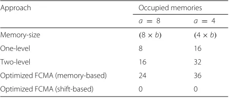
Table 2Occupied memories that are used by RNS-based DB2
DWT approaches. The input word length,w, is 16 bits and b=3∗n+1
Optimized FCMA (memory-based) 24 36
Optimized FCMA (shift-based) 0 0
For instance, three-channel DB2 implementation requires
9 MA blocks to sum up the final result, and in totalP7
RNS-based implementation has a total of 49 MA blocks
whenw = 16 anda = 4 bits.
If the FCMA of the second stage is implemented by means of memory, then each unit requires(q∗(( na)−1))
In contrast, if the FCMA of the second stage is imple-mented by rewiring the input of the first stage, then each tap requires at mostq∗(n−1)MAs, wherenis the chan-nel width. However, not all of these MAs are required, because the shift operations are applied to the binary ones of the filter coefficients. For example, from Table 1, h0
equal to(757)10 or(01011110101)2. This means that the
proposed approach requiresq(n¯−1)= 3∗6=18 mod-ulo adders, wheren¯is the average of binary ones inhj∗2z.
Table3summarizes the number of memories and MAs of
each implementation, respectively.
It is clear that as(w/a) increases, the number of MA increases because(w/a−1)MA are required to construct MA tree. Hence, the critical path delay (PSD) involves one multiplier followed bylog2(w/a−1)levels MA tree. As a consequence, there is a trade-off between the number of memory and its size on the overall performance of the system.
4 Simulation results, performance analysis, and validation
In the previous section, we have demonstrated the design of the DWT by using a residue number system. The two-level DWT RNS-based has been designed, implemented and tested with series of simulations to verify the DWT functionality. Experiments were carried out on the Xilinx
ZC706 evaluation board [45]. The performance of the
proposed approach was compared with the distributed
arithmetic (DA) [3], which is a multiplierless DWT.
We also considered the direct DWT implementation
Table 3Memory usage and adders for RNS-based approaches
Table 4FPGA resource utilization and system performance for the RNS components— i.e., FCMA and reverse converter
Resources (n=7) (n=10) n=10 n=13 n=10
FCMA RBC FCMA RBC S-FCMAc M-FCMA
Number of slice LUTs 234 114 335 143 731 999 348
Number of slice registers 375 148 478 187 792 1024 471
Number of occupied slices 121 55 158 57 360 524 164
Number of RAMB18E1 8 0 8 0 0 0 24
Output word length (bits) 22 0 31 0 31 40 31
Worst negative slack (ns) 7.3 7.2 7.1 7.29 7.23 7.26 7.29
Max. operating freq (MHz) 367.1 353.7 346.6 369.7 360.1 365.7 368.9
Data path delay (ns) 2.599 2.65 2.66 2.5 2.76 2.7 2.65
Estimated power (mW)a 25 3 29 3 6 7 21
Block RAM power (mW) 16 0 16 0 0 0 16
Latency (CC)b 5 6 5 5 6 6 5
aThe IO power estimation is not considered bClock cycle
cRewiring the input for implementing shift operations and a series of MAs. The FCMA involves the forward converters and modulo adders. “S-FCMA” is the shift-based FCMA,
the one that rewires the input, and “M-FCMA” is the memory-based FCMA
using an IP FIR Compiler 6.3 (FIR6.3) block, which provides a common interface to generate highly parameterizable, area-efficient, high-performance FIR filters [46].
In the following experiments, the moduli sets ofP7 =
{127, 128, 255},P10 = {1023, 1024, 2047}, and P13 =
{8191, 8192, 16383} were used. The dynamic range
of these sets are M=4161536, 2144338944, and
1099310309376, respectively. In fact, the moduli sets of
P10 and P13 are selected because their dynamic range
are greater than tho. For instance, Eq. 15 shows that
tho = 1279020283 for P10 with y = 6,z = 11, and
(hi) = 1.5436. In all RNS-based implementations, the
input word length was set to 16 bits.
4.1 Resource utilization and system performance
Table 4 summarizes the resource use by RNS-based
components— i.e., FCMA and reverse-binary converter
(RBC) when using 2×bmemory, where ‘b’ is the output
word length of Pn and equal to (3 ∗n+ 1). The
two-level, three-channel RNS contains two FCMA units and
3 different MAs (Fig.5b). The RBC unit consumes fewer
resources and less power with the operating frequency in all models being approximately equal and as high as 350 MHz or more. The optimized shift-based FCMA con-sume less power but the number of occupied slices is doubled compared to the memory-based implementation. Finally, it is clear that the BRAM consumes most power in all memory-based models (approximately 16 mW).
Table 5FPGA resource utilization and system performance of two-level DB2 DWT implementation with ZC706
RNS-based
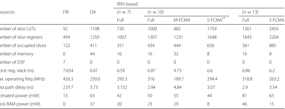
Resources FIR DA (n=7) (n=10) (n=13)
Full Full M-FCMA S-FCMA** Full S-FCMA
Number of slice LUTs 92 1108 730 1000 882 1759 1261 2455
Number of slice registers 494 1250 1007 1307 1231 1648 1643 2204
Number of occupied slices 122 411 351 434 444 656 561 885
Number of memory 0 44 16 16 32 8 16 8
Number of DSP 7 0 0 0 0 0 0 0
Worst neg. slack (ns) 7.654 6.01 6.59 6.87 4.73 6.6 6.86 6.2
Max. operating freq (MHz) 426.3 250.6 293.3 316 189.7 294.4 318.8 263.2
Data path delay (ns) 2.017 3.73 3.152 2.94 4.84 3.07 2.9 3.54
Estimated power (mW) 13 63 42 50 55 44 81 63
Block RAM power (mW) 0 37 20 23 29 8 46 15
Table 6The effect of using four memories in each filter-tap with ZC706
RNS-based
Resources DA (n=7) (n=10) (n=13)
Full Full M-FCMA S-FCMA** Full S-FCMA
Number of memory 44 32 32 52 16 32 16
Output word length (bits) 22 22 31 31 31 40 40
Estimated power (mW) 78 70 85 88 60 142 92
Block RAM power (mW) 51 39 43 49 18 88 36
**“S-FCMA” is the shift-based FCMA, the one that rewires the input, and “M-FCMA” is the memory-based FCMA
4.2 Two-level DWT evaluation
Table5lists the resource consumption and the system per-formance for the two-level DWT implementations when two memory elements are used in each filter-tap. The FIR-based model shows better performance compared to all multiplierless architectures but it requires several
multiplier units, known as DSP48E in modern FPGA [45].
It is also observed that the maximum frequency of all RNS-based schemes is higher than DA-based
DWT. Because the only change amongP7, P10, and P13
implementations is the moduli-set width, the maximum operating frequencies slightly changes among these designs. Furthermore, the two-level DB2 filter bank was designed with maximum operating frequencies between 260 and 360 MHz for full and optimized shift-based
FCMA, respectively. However,P7RNS-based is the only
model that has less resources compared to DA-based because of its small word length.
Furthermore, Table 5 shows that the RNS schemes
consume less power compared to DA-based DWT. The exception is that the Full model ofP13, which occurred due
to the hardware usage and the memory-size—i.e., 8×40.
The large size of the memory can further be split into
smaller memory (as shown in Fig. 5). Table 6 presents
the impact of using four-memory in each filter-tap on the power. It is obvious that the power consumption is increased as the number of memory and its size increase. The proposed shift-based RNS model compared to these models showed a better performance regards to power and maximum operating frequency. In spite of the defi-ciency in terms occupied slices, the proposed model has less number of memories and multipliers compared to DA- and FIR-based schemes.
4.3 Functionality verification
In this experiment, a sinusoidal signal is applied on each approach to verify the functionality of each design.
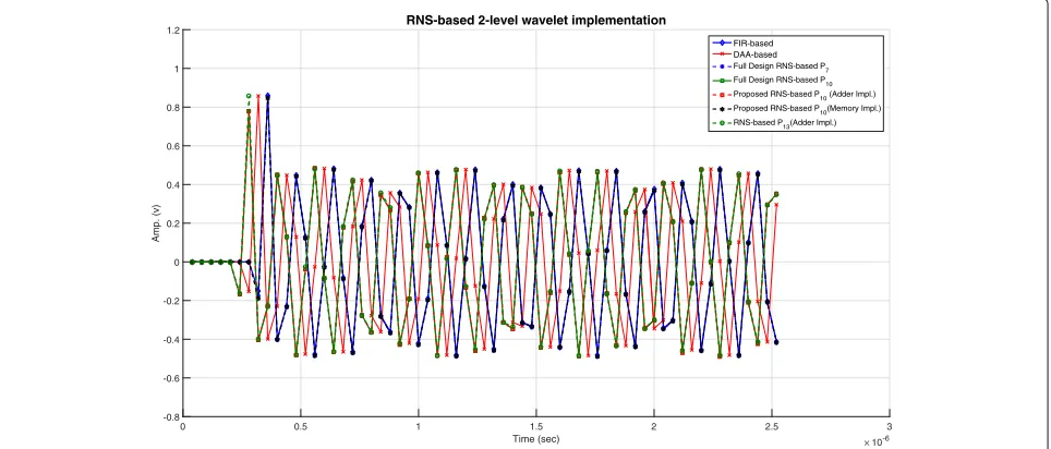
Figure9shows a comparison among all RNS-based
imple-mentations with FIR- and DA-based impleimple-mentations. It indicates that the proposed approaches are ahead of other implementations. To be more accurate, the two-level DB2 DWT implementations were simulated by DSP Logic
Analyzer and the result is shown in Fig. 10. It depicts
that the signals resulting from Full RNS- and FIR-based
3 5
. 2 2
5 . 1 1
5 . 0 0
Time (sec) 10-6
-0.8 -0.6 -0.4 -0.2 0 0.2 0.4 0.6 0.8 1 1.2
Amp. (v)
RNS-based 2-level wavelet implementation
FIR-based DAA-based Full Design RNS-based P
7
Full Design RNS-based P10
Proposed RNS-based P10 (Adder Impl.)
Proposed RNS-based P
10(Memory Impl.)
RNS-based P
13(Adder Impl.)
Fig. 10The output of two-level DWT using DSP Logic Analyzer when a sin wave is applied. Each clock cycle is 10 ns
lag behind the proposed architecture by 80 ns or 8 clock cycles, whereas the signal resulting from DA-based lags by 4 clock cycles.
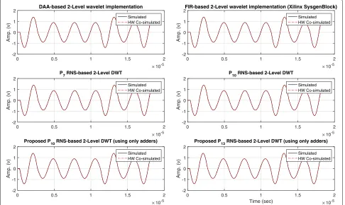
Eventually, we have verified the simulated result on ZC706 development kit and the simulation and hardware co-simulation results of the two-level DB2 implementa-tions are highly correlated, as shown in Fig.11.
4.4 Precision analysis
Generally, convolution-based DWT involves floating-point operations, which introduces rounding errors. Because the filter-banks coefficients, designing by means of floating-point, require large hardware resources to
retain the precision, we replaced the floating-point method with RNS numbering system. We simply multi-plied the input by 2yand the filter coefficients by 2z. At the
end, we converted the result back to floating-point num-ber. PSNR is the most commonly used method to measure the quality of the result. In fact, it measures the peak error and high PSNR means better quality and that less error is introduced to the result.
We carried out the precision analysis for the first and second levels. The Daubechies wavelet with four coeffi-cients were used and the result of each level was compared with the actual double-precision values via MATLAB.
Table 7shows the behavior of the proposed approaches
0 0.5 1 1.5 2
10-5 -2
-1 0 1 2
Amp. (v)
DAA-based 2-Level wavelet implementation
Simulated HW Co-simulated
0 0.5 1 1.5 2
10-5 -2
-1 0 1 2
Amp. (v)
FIR-based 2-Level wavelet implementation (Xilinx SysgenBlock)
Simulated HW Co-simulated
0 0.5 1 1.5 2
10-5 -2
-1 0 1 2
Amp. (v)
P
7 RNS-based 2-Level DWT
Simulated HW Co-simulated
0 0.5 1 1.5 2
10-5 -2
-1 0 1 2
Amp. (v)
P
10 RNS-based 2-Level DWT
Simulated HW Co-simulated
0 0.5 1 1.5 2
10-5 -2
-1 0 1 2
Amp. (v)
Proposed P10 RNS-based 2-Level DWT (using only adders)
Simulated HW Co-simulated
0 0.5 1 1.5 2
Time (sec) 10-5
-2 -1 0 1 2
Amp. (v)
Proposed P13 RNS-based 2-Level DWT (using only adders)
Simulated HW Co-simulated
Table 7The PSNR values of one- and two-level of different DWT implementations
DA FIR RNS Optimized RNS
P7 P10 P13 P10a P13a
Architecture 1L/2L 1L/2L 1L/2L 1L/2L 1L/2L 2L 2L
Input precision Q5,16 Q5,16 y=8/8b y=12/12 y=13/12 y=6 y=11
Coeff. precision Q1,15c Q0,15 z=11 z=16/11 z=18/13 z=11 z=13
Internal word length 22 bit NA 22 bit 31 bit 40 bit 31 bit 40 bit
PSNR (dB) 73.5/63.5 86.3/78.7 56.5/41.87 84/53 90/54 48.5d 54.5
aOptimized FCMA model, where one RBC is used bThe input to RNS circuit is 16-bit unsigned integer cMemory word length
dThis is the only combination that satisfies Eq. (16)
in terms of input and wavelet coefficients precision. The output precision is set toQ5,16for all implementations. It
is worth noting that employing the memory-based FCMA or shift-based FCMA at the second level has no effect on the output because both schemes compute identical results.
The optimized two-level withP10has a maximum input
scaling factor of 6 (due to Eq. 16). As a consequence,
we cannot adapt their scaling factors. In contrast, the optimized two-level ofP13has higher input and filter coef-ficients scaling factors due to its large word length, which enables it to have large accuracy values.
Table7presents that the maximum achieved PSNR of
P7set is 56.5 dB and 41.87 for the first and second level,
respectively. We could not achieve better accuracy with
the specified scaling factors becausey+z+3 = 21 ≤
(3∗7)+1 = 22 (see Eq.16). If an application requires higher accuracy values, then different moduli set with largenshould be selected. Figure12compares the effect of changing the scaling factors of two different moduli sets,
P10andP13for one-level DB2 RNS-based approach. The
input scaling factor was varied between 8-bit and 13-bit, and filter scaling factor was varied between 11 and 18.
As expected, lower scaler factors produces PSNR equal to 60 dB. While the maximum PSNR equal to 90.37 is
obtained with y = 13 and z = 18 for P13, the
maxi-mum PSNR ofP10is obtained wheny = 12 andz = 16
(Eq. (12)). It is worth mentioning that as the filter scaling factor increases, no hardware cost is added to the design, because all the changes correspondingly occurred in the memory contents. Figure13shows the effect of the scaling factors for two-level DB2 RNS-based approach. The
pro-posed 2-stage RNS-basedP13withz=13, has maximum
PSNR of 54.5 dB, which is roughly equal to the full model
withz=11.
5 Conclusions
In this article, we have addressed the development of a multiplierless scheme for two-level RNS-based DWT, which can be adapted to any moduli set, with any num-ber of channel. This approach intensively use memory to speed up the entire processing time. In order to achieve low latency, we incorporated two novel ideas into the two-level proposed design, as follows: (1) eliminating the intermediate RBC unit; (2) replacing the internal memory of the second level by simple circular shift operations. A
(a)
(b)
Fig. 13The impact of input,y, and wavelet filter coefficients,z, scaling factors of two-level RNS-based implementation with respect toP10andP13
moduli sets on PSNR
key feature of this approach is that the user can change the scaling factors,yandz, either to achieve high PSNR values or lowering the PSNR value in order to design multi-level DWT with low latency.
The trade-off between system performances and resource consumption was addressed. Experiment results showed that the RNS-based approach would be more appropriate for multi-level DWT because the number of memory element is always constant as the number of level is increased. In addition, it is observed that the proposed RNS-based DWT implementation has lower
latency than FIR and Pn RNS-based implementations.
Finally, an acceptable precision can be achieved by adapt-ing the scaladapt-ing factors. Table8indicates the advantage and disadvantages of each moduli-set.
Given the implementation examples for experimental verifications and analysis, the approach was validated on a ZYNQ ZC706 development kit. The co-simulation results have also been verified and compared with the simulation environment. The complexity and optimization of multi-level DWT with respect to hardware structure provides a foundation for employing an appropriate algorithm for high-performance applications, such as in cognitive
communication, where DWT analysis is combined with machine learning algorithms.
Appendix 1 Acronyms
BRAM Block RAM
BRC Binary-to-residue converter
CC Clock cycle
CLB Configurable logic block
CPD Critical path delay
CRT Chinese reminder theorem
CSE Common subexpression elimination
DA Distributed arithmetic
DSP Digital signal processing
DWT Discrete wavelet transform
GCD Greatest common divisor
GE Graph-based eliminations
FCMA Forward-converter and modular adders
FIR Finite impulse response
FPGA Field-programmable gate array
LS Lifting-based scheme
LUT Look-up table
MA Modular adder
Table 8A comparison between RNS-based implementations using moduli-setPn
P7 P10 P13
Pros •Design is simple
•Consume less power •
Design is moderate
•The shift-based scheme has lower latency and consume less power
•Can be extended to three-level (withy=8 andz=9)
•The shift-based scheme has lower latency and consume less power
Cons •Low PSNR
• Cannot be extended to multi-level DWT
• Cannot be extended to
three-level DWT •
MAC Multiplier-accumulator
MCM Multiple constant multiplications
PSNR Peak signal-to-noise ratio
RBC Reverse-binary converter
RNS Residue number system
Appendix 2
Mathematical symbols
a×b The memory word size
l Number of DWT levels
M The maximum range ofPn
N Number of filter tap
hk The low-passkthfilter coefficient
m The number of magnitude bits
mi Theithmoduli ofPn
n The moduli set base (e.g.P7)
q Number of RNS channel
τ Latency
w Word length
y The input scaling factor
z The filter scaling factor
Acknowledgements
The authors would like to thank the anonymous reviewers for their valuable comments and suggestions to improve the quality of the article.
Authors’ contributions
All authors contributed to the work. Both authors read and approved the final manuscript.
Competing interests
The authors declare that they have no competing interests.
Publisher’s Note
Springer Nature remains neutral with regard to jurisdictional claims in published maps and institutional affiliations.
Received: 11 October 2017 Accepted: 30 May 2018
References
1. P Yang, Q Li, Wavelet transform-based feature extraction for ultrasonic flaw signal classification. Neural Comput. & Applic.24(3-4), 817–826 (2014)
2. SK Madishetty, A Madanayake, RJ Cintra, VS Dimitrov, Precise VLSI architecture for AI based 1-D/ 2-D Daub-6 wavelet filter banks with low adder-count. IEEE Trans. Circ. Syst. I Regular Papers.61(7), 1984–1993 (2014) 3. M Martina, G Masera, MR Roch, G Piccinini, Result-biased
distributed-arithmetic-based filter architectures for approximately computing the DWT. IEEE Trans. Circ. Systems I Regular Papers.62(8), 2103–2113 (2015) 4. H Alzaq, BB Ustundag, inEuropean Wireless 2015; 21th European Wireless
Conference; Proceedings Of. Wavelet Preprocessed Neural Network Based Receiver for Low SNR Communication System (VDE, Budapest, 2015), pp. 1–6
5. N Carta, D Pani, L Raffo,Impact of Threshold Computation Methods in Hardware Wavelet Denoising Implementations for Neural Signal Processing. (Springer, Cham, 2015), pp. 66–81. http://doi.org/10.1007/978-3-319-26129-4_5
6. S Mallat,A Wavelet Tour of Signal Processing, Third Edition: The Sparse Way, 3rd edn. (Academic Press, Philadelphia, PA, USA, 2008)
7. M Vetterli, C Herley, Wavelets and filter banks: theory and design. IEEE Trans. Signal Process.40(9), 2207–2232 (1992)
8. S Gnavi, B Penna, M Grangetto, E Magli, G Olmo, Wavelet kernels on a DSP: a comparison between lifting and filter banks for image coding. EURASIP J. Adv. Signal Process.2002(9), 458215 (2002)
9. I Daubechies, W Sweldens, Factoring wavelet transforms into lifting steps. J Fourier Anal. Appl.4(3), 247–269 (1998)
10. M MAB, NM Sk, in2018 31st International Conference on VLSI Design and 2018 17th International Conference on Embedded Systems (VLSID). An efficient vlsi architecture for convolution based dwt using mac (IEEE, Pune, 2018), pp. 271–276.https://doi.org/10.1109/VLSID.2018.75 11. A Gacic, M Puschel, JMF Moura, in2004 IEEE International Conference on
Acoustics, Speech, and Signal Processing. Automatically generated high-performance code for discrete wavelet transforms, vol 5 (IEEE, Montreal, 2004), pp. 69–725.https://doi.org/10.1109/ICASSP.2004. 1327049
12. E Ramola, JS Manoharan, in2011 3rd International Conference on Electronics Computer Technology. An area efficient vlsi realization of discrete wavelet transform for multiresolution analysis, vol 6 (IEEE, Kanyakumari, 2011), pp. 377–381
13. I Mamatha, S Tripathi, TSB Sudarshan, in2017 International Conference on Computing, Communication and Automation (ICCCA). Convolution based efficient architecture for 1-d dwt (IEEE, Greater Noida, 2017),
pp. 1436–1440.https://doi.org/10.1109/CCAA.2017.8230023 14. M I, S Tripathi, S TSB, in2016 3rd International Conference on Signal
Processing and Integrated Networks (SPIN). Pipelined architecture for filter bank based 1-d dwt (IEEE, Noida, 2016), pp. 47–52.https://doi.org/10. 1109/SPIN.2016.7566660
15. PK Meher, BK Mohanty, MMS Swamy, in2015 28th International Conference on VLSI Design. Low-Area and Low-Power Reconfigurable Architecture for Convolution-Based 1-D DWT Using 9/7 and 5/3 Filters (IEEE, Bangalore, 2015), pp. 327–332.https://doi.org/10.1109/VLSID.2015.61
16. J Ramírez, A García, PG Fernandez, A Lloris, in2000 10th European Signal Processing Conference. An efficient rns architecture for the computation of discrete wavelet transforms on programmable devices (IEEE, Tampere, 2000), pp. 1–4
17. L Aksoy, P Flores, J Monteiro, A tutorial on multiplierless design of FIR filters: algorithms and architectures. Circ. Syst. Signal Process.33(6), 1689–1719 (2014)
18. Y Voronenko, M Püschel, Multiplierless multiple constant multiplication. ACM Trans. Algorithm.3(2) (2007)
19. F Al-Hasani, MP Hayes, A Bainbridge-Smith, A common subexpression elimination tree algorithm. IEEE Trans. Circ. Syst. I Regular Papers.60(9), 2389–2400 (2013)
20. X Lou, YJ Yu, PK Meher, New approach to the reduction of sign-extension overhead for efficient implementation of multiple constant
multiplications. IEEE Trans. Circ. Syst. I Regular Papers.62(11), 2695–2705 (2015)
21. H Liu, A Jiang, in2016 8th International Conference on Wireless Communications Signal Processing (WCSP). Efficient design of fir filters using common subexpression elimination (IEEE, Yangzhou, 2016), pp. 1–5.https://doi.org/10.1109/WCSP.2016.7752701
22. L Aksoy, P Flores, J Monteiro, Multiplierless design of folded dsp blocks. ACM Trans. Des. Autom. Electron. Syst.20(1), 14–11424 (2014) 23. A Peled, B Liu, A new hardware realization of digital filters. IEEE Trans.
Acoust. Speech Signal Process.22(6), 456–462 (1974) 24. DJ Allred, W Huang, V Krishnan, H Yoo, DV Anderson, in
Field-Programmable Custom Computing Machines, 2004. FCCM 2004. 12th Annual IEEE Symposium On. An FPGA Implementation for a High Throughput Adaptive Filter using Distributed Arithmetic (IEEE, Napa, 2004), pp. 324–325.https://doi.org/10.1109/FCCM.2004.15 25. H Yoo, DV Anderson, inProceedings. (ICASSP ’05). IEEE International
Conference on Acoustics, Speech, and Signal Processing, 2005. Hardware-efficient Distributed Arithmetic Architecture for High-Order Digital Filters, vol 5 (IEEE, Philadelphia, 2005), pp. 125–1285.https://doi. org/10.1109/ICASSP.2005.1416256
26. H Alzaq, BB Üstünda ˘g, in2017 10th International Conference on Electrical and Electronics Engineering (ELECO). Multiplier-less 1-level discrete wavelet transform implementations on zc706 development kit (IEEE, Bursa, 2017), pp. 1122–1126
28. W Jenkins, B Leon, The use of residue number systems in the design of finite impulse response Digital Filters. IEEE Trans. Circ. Syst.24(4), 191–201 (1977)
29. CH Chang, AS Molahosseini, AAE Zarandi, TF Tay, Residue number systems: a new paradigm to datapath optimization for low-power and high-performance digital signal processing applications. IEEE Circ. Syst. Mag.15(4), 26–44 (2015)
30. J Ramírez, U Meyer-Bäse, F Taylor, A García, A Lloris, Design and implementation of high-performance RNS wavelet processors using custom IC technologies. J. VLSI Signal Process. Syst. Signal Image Video Technol.34(3), 227–237 (2003)
31. GC Cardarilli, A Nannarelli, M Petricca, M Re, in2015 IEEE 58th International Midwest Symposium on Circuits and Systems (MWSCAS). Characterization of RNS multiply-add units for power efficient DSP (IEEE, Fort Collins, 2015), pp. 1–4.https://doi.org/10.1109/MWSCAS.2015.7282052
32. R Conway, J Nelson, Improved RNS FIR filter architectures. IEEE Trans. Circ. Syst. II Express Briefs.51(1), 26–28 (2004)
33. I Daubechies,Ten Lectures on Wavelets. (Society for Industrial and Applied Mathematics, Philadelphia, 1992)
34. KH Rosen,Elementary Number Theory and Its Applications, 5th edn. (Addison-Wesley, Reading, MA, 2004), p. 638
35. PVA Mohan, RNS-to-binary converter for a new three-moduli set
2n+1−1, 2n, 2n−1. IEEE Trans. Circ. Syst. II Express Briefs.54(9), 775–779 (2007)
36. S-H Lin, M-h Sheu, C-H Wang, Y-C Kuo, inCircuits and Systems, 2008. APCCAS 2008. IEEE Asia Pacific Conference On. Area-Time-Power Efficient VLSI Design for Residue-to-binary Converter Based on Moduli Set
(2n, 2n+1−1, 2n+1)(IEEE, Macao, 2008), pp. 168–171.https://doi.org/ 10.1109/APCCAS.2008.4745987
37. KS Reddy, S Bajaj, SS Kumar, inTENCON 2014 - 2014 IEEE Region 10 Conference. Shift add approach based implementation of RNS-FIR filter using modified product encoder (IEEE, Bangkok, 2014), pp. 1–6.https:// doi.org/10.1109/TENCON.2014.7022321
38. CH Vun, AB Premkumar, W Zhang, A new RNS based DA approach for inner product computation. IEEE Trans. Circ. Syst. I Regular Papers.60(8), 2139–2152 (2013)
39. A Hariri, K Navi, R Rastegar, A new high dynamic range moduli set with efficient reverse converter. Comput. Math. Appl.55(4), 660–668 (2008) 40. B Cao, T Srikanthan, C-H Chang, Efficient reverse converters for the
four-moduli sets(2n−1, 2n, 2n+1, 2n+1−1)and(2n−1, 2n, 2n+1, 2n−1−1). IEE Proc. Comput. Digit Tec.152(5), 687–696 (2005)
41. B Cao, C-H Chang, T Srikanthan, An efficient reverse converter for the 4-moduli set2n−1, 2n, 2n+1, 22n+1based on the new Chinese remainder theorem. IEEE Trans. Circ. Syst. I Fundam. Theory Appl.50(10), 1296–1303 (2003)
42. R Zimmermann, inProceedings 14th IEEE Symposium on Computer Arithmetic (Cat. No.99CB36336). Efficient vlsi implementation of modulo (2n plusmn;1) addition and multiplication (IEEE, Adelaide, 1999), pp. 158–167.https://doi.org/10.1109/ARITH.1999.762841 43. L Kalampoukas, D Nikolos, C Efstathiou, HT Vergos, J Kalamatianos,
High-speed parallel-prefix modulo2n−1adders. IEEE Trans. Comput. 49(7), 673–680 (2000)
44. G Dimitrakopoulos, DG Nikolos, HT Vergos, D Nikolos, C Efstathiou, in2005 12th IEEE International Conference on Electronics, Circuits and Systems. New architectures for modulo2n−1adders (IEEE, Gammarth, 2005), pp. 1–4. https://doi.org/10.1109/ICECS.2005.4633502
45. Xilinx Inc., Zynq-7000 All Programmable SoC ZC706 evaluation kit. https://www.xilinx.com/products/boards-and-kits/ek-z7-zc706-g.html. Accessed 30 Aug 2017
46. Xilinx: LogiCORE IP FIR Compiler v6.3. Product Specification DS795 (Oct 2011).http://www.xilinx.com/support/documentation/ip_