ISSN(Online): 2319-8753 ISSN (Print): 2347-6710
I
nternational
J
ournal of
I
nnovative
R
esearch in
S
cience,
E
ngineering and
T
echnology
(A High Impact Factor, Monthly, Peer Reviewed Journal) Visit: www.ijirset.com
Vol. 7, Issue 2, February 2018
Design and Implementation of Grid Integrated
wind and Solar PV System Using Lattice
Digital Filter
Dr.R.Arulmozhiyal, M.E ., Ph.D., Sandhiya.R,
Professor And Head ( Sona Pedac R&D Center), Department of EEE, Sona College of Technology, Salem, India.
M.E. Student, Department of EEE, Sona College of Technology, Salem, India.
ABSTRACT: A novel architecture for a lattice digital ladder filter (LDLF) is presented. The design of the proposed filter is based on a low-sensitive bilinear transformation of analogue ladder filters where the delay-free loops are eliminated. The proposed filter is very efficient, as it gives a sharp amplitude response with a small number of multipliers. It also has a low sensitivity to round-off noise, and good stability properties. A 5th order elliptic filter has been realized for the digital I/Q up/down conversion stage in an OFDM-based WLAN chip using a 0.35µm CMOS process. The design has a power consumption of 137mW and occupying an area equivalent to 5.6kgates.
KEYWORDS: Asynchronous generators, machine control, rotors, wind turbines
I. INTRODUCTION
In almost all applications filtering is necessary in the processing of signals. For the digital signal processing part digital filters are needed. Most implementations today use Finite Impulse Response (FIR) filters due to several reasons: Ease of understanding and design, always stable, efficient implementations when combined with interpolation and decimation by large factors, etc. The choice of FIR filters does not always lead to the most efficient implementations though. For many applications the area and power penalty can be very large, compared to other implementations.
A natural alternate choice is using Infinite Impulse response (IIR) filters. However, using schoolbook methods for design of IIR filters, often leads to very discouraging experiences. Examples of unpleasant results are unstable filters and limit cycles of various natures. In this paper a versatile design of an LDLF IIR filter is described, which with proper design methods avoids the problem mentioned above and combined with an efficient area and low power consumption.
II. OVERVIEW OF LATTICE DIGITAL LADDER FILTER
The filter chosen is a simplification of the Bilinear Digital Ladder Filter (BDLF) [1] filter family, namely the Lattice version [2][3], having a canonical number of multipliers. In the following, the filters in this family will be denoted Digital Ladder Filters (DLFs), and specifically Lattice DLFs (LDLF).
ISSN(Online): 2319-8753 ISSN (Print): 2347-6710
I
nternational
J
ournal of
I
nnovative
R
esearch in
S
cience,
E
ngineering and
T
echnology
(A High Impact Factor, Monthly, Peer Reviewed Journal) Visit: www.ijirset.com
Vol. 7, Issue 2, February 2018
III. FILTER SPECIFICATIONS
The proposed digital filter is used for separation of the real (“in phase” or “I”) and imaginary (“quadrature phase” or “Q”) parts of the real input signal to a digital WLAN modem. The received OFDM input signal is centered around a low digital-IF frequency of 15 MHz.
Figure 1 IQ demodulator architecture
In the architecture shown in Figure 1, we have an ADC sampling at 60 MHz. The negative frequency components of the IQ-modulated signal are filtered in the complex band-pass filter (BPF) in order to make the separation of I and Q channels. Finally, the signal after the filter is decimated and mixed into the baseband. The pass-band is centered in the middle of the positive frequency band at 15 MHz (i.e. at ¼ of the sampling frequency).
The spectral mask for the OFDM symbol with 64 subcarriers defined in Hiperlan2 standard [4] is shown in Figure 1. If the subcarriers are numbered from –32 to 31 (inclusive), the numbers from –32 to –28, 28 to 31 at the edges are not used. This part of the spectral mask can be used for the filter roll-off.
Figure 1 Spectral mask of the OFDM symbol
The pass-band of the filter is chosen from 6.6 MHz to 23.4 MHz. The passband ripple should be less than 0.5 dB and the group-delay spread less than 4.8 samples. 4.8 samples correspond to 10% of the cyclic prefix, which are 16 symbols. For the rejection of the negative frequency components from –23.4 MHz to –6.6 MHz, we require attenuation of 45 dB so that they contribute interference negligible compared to the noise level of the analog-to-digital converter. For the rejection of adjacent channel interference at frequencies below 3.4 MHz and above 28.6 MHz we require an attenuation of more than 35 dB. Seven bits (including sign) for the coefficients were found sufficient to fulfil the requirements.
Fs / 2 = 10 MHz.
zero carriers 4
zero carriers 3
5zero carriers I, Q
carriers
32 31 carriers
Frequency 1carrier at DC
ADC complex
BPF
down-sampling by 3
exp(j2 5 MHz t )
ISSN(Online): 2319-8753 ISSN (Print): 2347-6710
I
nternational
J
ournal of
I
nnovative
R
esearch in
S
cience,
E
ngineering and
T
echnology
(A High Impact Factor, Monthly, Peer Reviewed Journal) Visit: www.ijirset.com
Vol. 7, Issue 2, February 2018
IV. FILTER IMPLEMENTATION
The filter dimensioning is done by first considering a real low-pass filter, and then transposing the center frequency from DC to the desired value. From the shifting property of the z-transform it follows that this is achieved by placing a multiplication by c=exp(j2π fcenter/fsampling) in series with each time-delay.
For the real low-pass prototype an elliptic lattice bilinear ladder filter is used as it gives sharp amplitude response with less hardware resources. It also has a low sensitivity to round-off noise and good stability properties. An apparent disadvantage is that an elliptic filter normally has a strong non-linear phase response. However, the non-linear phase response is mostly limited to frequencies close to the cut-off frequencies. Thus, if the amplitude response is sharp enough that the cut-off frequencies may be placed somewhat outside the required pass-band, it is still possible to satisfy linear phase requirements in the required passband.
Figure 2 Signal flow diagram for 5th order LDLF
The architecture of the elliptic lattice bilinear ladder filter is shown in Figure 2. A complex multiplier is placed in series with each time-delay. It was found that a 5th order filter was needed to meet the specifications. The filter has two multiplications in each loop, one by a real filter coefficient and one by a complex multiplier. It is possible to move the complex multipliers out from their original positions at the time delays. The real multiplication by a filter coefficient is then absorbed by a complex multiplication, and each loop contains only one (complex) multiplication. However, this is not done in the described implementation. In the filter considered here we have the special case that the center frequency is exactly one quarter of the sampling frequency. The complex multiplier is therefore purely imaginary: c=j, which represents a rotation by π/2 as shown by:
Signal quantization in the filter refers to the reduction of word length needed after addition and multiplication operations, and overflow handling refers to what is done after addition operation resulting in a value which exceeds the permitted number interval.
4.1. Overflow handling
ISSN(Online): 2319-8753 ISSN (Print): 2347-6710
I
nternational
J
ournal of
I
nnovative
R
esearch in
S
cience,
E
ngineering and
T
echnology
(A High Impact Factor, Monthly, Peer Reviewed Journal) Visit: www.ijirset.com
Vol. 7, Issue 2, February 2018
With this simplification, the hardware cost from the rotators has been eliminated. For the hard-limiters, the design complexity requires a multiplexer and a comparator. Based on the value of the comparison either the threshold value or the operand is passed as a result of the multiplexing process. We have introduced the threshold values to be set as 0.11…11 for maximum positive and 1.00...01 for minimum negative after the comparison. Moreover, the number just before the hard limiting process is compared only with 01. (+1) and 11. (-1) at the comparator inputs in order to reduce the critical path of the design significantly.
The signals treated by the filter are wide-band, the overflow limit (i.e. the number of integer bits) can be determined by the L2-norm of the filter response from the input to the given quantization point. The L2-norms were calculated as 0.95, 2.04, and 1.54 for the upper ladder, and 0.93 and 1.53 for the lower. All the bits from the input are considered being fractional, except for the sign bit. Thus the number of integer bits (not including the sign bit) are chosen as 0, 1, and 1 for the upper ladder, and 0 and 1 for the lower.
4.2. Signal rounding
Signal rounding points are located at two points, one after the multiplication of the signal, and one just before the hard-limiter.
After the multiplication of the signal by the coefficients, discarding the last bits in the resulting twos complement signal performs quantization. This is equivalent to “round-off towards -1”. The quantization point directly after the multiplication should not introduce too much extra noise, as long as the signal word length is still much larger than the quantization point just before the hard-limiter. This quantization will reduce the hardware overhead of the adders. The number of integer bits is still dimensioned so that overflow will not occur.
The second rounding point is located just before the hard limiter i.e. “round-off towards 0” is performed at this rounding point. We have introduced a comparator just before the rounding in order to round the negative numbers towards zero. For this the rounded signal is first rounded to a value with additional fractional bit added to its target word length. This value is compared with – 0.00…001 which is at the same word length of the generated rounded value. If this value is equal to that small negative value then this value is truncated into zero.
The number of fractional bits is chosen from the amplitude response from the quantization points to the filter output. The maximum peak gains from the five nodes are +1, -5, -3, +2, and -3 decibels, respectively.
We want the noise power generated by round-off in the quantization nodes in the filter to be small compared to the quantization noise power generated by an ideal 8 bits ADC (i.e. an ADC with 7 fractional bits). If we have only one quantization point and if the gain at this point is 0 dB, we have chosen 8 fractional bits at the quantization point. Since we do have 5 quantization points we choose the number of fractional bits as 9.3, 8.3, and 8.7 for the upper ladder, and 9.5 and 8.7 for the lower. This is, however, an overestimate of the number of bits. First, the maximum gain from each quantization node has been used. Second, a real 8 bit ADC generates more noise than an ideal one. In order to have negligible noise contributions from the filter compared to the ADC the following number of fractional bits was chosen: 11, 10, and 11 for the upper ladder, and 11 and 10 for the lower.
4.3. Implementation of the TX modulator
The same filter and mixer used for IQ demodulation can be used for the implementation of the IQ modulator architecture. The corresponding transmitter architecture is obtained by application of the transposition theorem.
As the bandwidth requirements are the same for TX and RX, the same filter can be used. An additional gain is inserted inside the filter to compensate for the energy loss due to the zeros inserted by the up-sampling module.
V. REALIZATION OF THE FILTER AND MEASUREMENTS
ISSN(Online): 2319-8753 ISSN (Print): 2347-6710
I
nternational
J
ournal of
I
nnovative
R
esearch in
S
cience,
E
ngineering and
T
echnology
(A High Impact Factor, Monthly, Peer Reviewed Journal) Visit: www.ijirset.com
Vol. 7, Issue 2, February 2018
The measured features of the LDLF based (de)modulator are summarized in Table 1 for a signal word length of 13 bits (including sign).
Table 1 Features of the IQ-(de)modulator
Technology 0.35µm CMOS 5LM Area of the filter 5163 gates
Area of mixer and decimator/interpolator
433 gates
Area of IQ-(de)modulator
5596 gates
Critical path timing 11.89 ns (84 MHz. ) Estimated power
dissipation
( for a broadband signal )
137 mW
Coefficient word length 7- bit (including sign ) Signal word length 13- bit (including sign ) Passband ripple 0.35 dB
Stopband attenuation
37 dB (at Nyquist frequency ) 48 dB (for adjacent mirror channel )
3-dB points 6.12 MHz, 23.88 MHz Group delay variation 4.5 samples
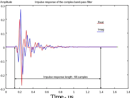
Impulse response length 66 samples
The impulse response, the transfer function and the group delay of the filter are shown in Figure 3, Figure 4 and Figure 5 respectively. The figures indicate a sampling frequency of 60MHz, but the actual measurements have been performed at 12MHz due to problems with power glitches on the (rather complex) evaluation board.
Time - us
Figure 3 Measured impulse response of the BPF -0.3
-0.2 -0.1 0 0.1 0.2 0.3
0 0.2 0.4 0.6 0.8 1 1.2 1.4 1.6 1.8
Impulse response length : 66 samples Impulse response of the complex band-pass filter
ISSN(Online): 2319-8753 ISSN (Print): 2347-6710
I
nternational
J
ournal of
I
nnovative
R
esearch in
S
cience,
E
ngineering and
T
echnology
(A High Impact Factor, Monthly, Peer Reviewed Journal) Visit: www.ijirset.com
Vol. 7, Issue 2, February 2018
Frequency (MHz)
Figure 4 Measured transfer function of the BPF
Frequency - MHz
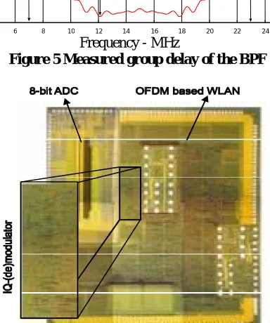
Figure 5 Measured group delay of the BPF
Figure 6 Chip microphotograph of WLAN modem 12
14 16 18 20 22 24
4 6 8 10 12 14 16 18 20 22 24 26
Group delay - Samples Samples
Fs = 60MHz
ISSN(Online): 2319-8753 ISSN (Print): 2347-6710
I
nternational
J
ournal of
I
nnovative
R
esearch in
S
cience,
E
ngineering and
T
echnology
(A High Impact Factor, Monthly, Peer Reviewed Journal) Visit: www.ijirset.com
Vol. 7, Issue 2, February 2018
VI. CONCLUSIONS
An area and power efficient implementation of up/down-conversion for an OFDM-WLAN modem has been described. The design utilises complex bandpass filters combined with simple down-sampling and mixing functions for the receiver. The implementation also supports the corresponding functions for the transmitter part of the modem. The bandpass filter uses only 7 bits for coefficients and 13 bits for signals (including sign bit), which is very area and power efficient compared to e.g. FIR implementations. The estimated maximum operating frequency exceeds 80MHz for the chosen 0.35um CMOS process. The demodulator design uses only 3.3% of the number of gates compared to the WLAN modem part.
VII. ACKNOWLEDGEMENTS
This work was performed in the frame of the ESPRIT Project-BANDIT, funded by the European Commission.
REFERENCES
[1] S. Signell, T. G. Kouyoumdjiev, K. H. Mossberg, “Design and Analysis of Bilinear Digital Ladder Filters”, IEEE Trans. on Circuits and Systems, Vol. 43 , No. 2., February 1996.
[2] L. Harnefors, J. Holmberg, M. Sollander, S. Signell; “Computationally Fast Lattice Bilinear Digital Ladder Filters with Comparison to Circulator WDF’s”, proceedings of ISCAS’98