ISSN(Online): 2319-8753 ISSN (Print) : 2347-6710
I
nternational
J
ournal of
I
nnovative
R
esearch in
S
cience,
E
ngineering and
T
echnology
(An ISO 3297: 2007 Certified Organization)
Vol. 5, Issue 6, June 2016
A Single-Switch Improved Valley-Fill Passive
Current Shaper for Compact Fluorescent
Lightings
G.Ramakrishnaprabu 1, Gunasekar 2
Associate Professor, Department of EEE, VMKV Engineering College, Salem, Tamilnadu, India1 P.G. Student, Department of EEE, VMKV Engineering College, Salem, Tamilnadu, India 2
ABSTRACT: The principle goal of this research is to reduce Total Harmonics Distortions of this nonlinear load
without active or passive filter installations. New generation of CFLs designed for reduce Total Harmonics Distortions with high power factor process and also available in higher price. Simple single switch electronic ballast with passive valley-fill power factor correction with EMI filter is proposed in this project for CFL application. The proposed single-switch ballast circuit is able to achieve zero current single-switching to maximize the circuit efficiency. A simple feedback circuit with duty ratio control is also proposed to improve the high lamp current crest factor caused by the valley-fill circuit. The output of this project, Total harmonics distortion is minimized, Power factor has been improved and the power loss of the above circuit has been minimized with minimum cost.
KEYWORDS:Total Harmonic Distortion (THD), Electro Magnetic Interference (EMI), EMI Filter, CFL
I. INTRODUCTION
With the global concerns regarding the conservation of the Earth’s limited energy resources, the use of compact fluorescent lamps (CFL) or energy-saving light bulbs is being imposed by the governments of a growing list of countries in an attempt to phase out conventional incandescent lamps to reduce energy usage. A single CFL consumes only one-third as much electricity as a standard incandescent lamp when providing the same light output. Hence, by using CFLs, consumers can save a large amount of money in the long-run with the reduced energy cost compared. Due to the size and cost constraint of a CFL, electronic ballast conventionally used in the CFL normally consists of a diode rectifier followed by a half-bridge self-oscillating resonant inverter; the type of resonant circuit that fluorescent lighting ballasts use is usually the typical LC resonant circuit. A major drawback of the aforementioned ballast circuit configuration is that the presence of the large dc-link capacitor limits the conduction time of the input current, which results in poor input power factor. By drawing an input line current with very low power factor, the line current is highly distorted. It is observed that the THD level increases exponentially and is inversely proportional to the power factor. The effect of the poor power factor from CFL on the utility can be illustrated from the following example. Although a single CFL consumes much less power than the incandescent lamp to provide the same luminous intensity, when a large quantity of incandescent lamp is replaced with CFL in the near future, the large amount of current harmonics produced by CFLs will become a severe problem for the utility and the power system network. Hence, it is necessary for the designers of CFL to incorporate power factor correction (PFC) function in its ballast design.
ISSN(Online): 2319-8753 ISSN (Print) : 2347-6710
I
nternational
J
ournal of
I
nnovative
R
esearch in
S
cience,
E
ngineering and
T
echnology
(An ISO 3297: 2007 Certified Organization)
Vol. 5, Issue 6, June 2016
II LITERATURE REVIEW
“Single Phase Converters for Power Factor Correction with Tight Output Voltage Regulation” K. Umamaheswari, V. Venkatachalam IJETA, ISSN 2250-2459, ISO 9001:2008 Certified Journal, Volume 3, Issue 2, February 2013
The fly back converter type single-stage converter and a half wave rectifier with time-multiplexing control (TMC) for power factor correction is proposed. It has the advantage of better magnetic core utilization and better performance for high power applications. The major portion of the input is transferred to the load through ac-dc conversion. And the part of the input power is delivered to the auxiliary output through the fly back conversion and stored in the capacitor. The voltage ripple of the main output can also be reduced. With TMC the power processes can be achieved by single transformer to reduce the cost and the size of the converter. The simulation result of the proposed converter presents, simplicity, high power factor with low cost and size.
“Simulation of high power factor single state LCC Resonant Inverter” Mohammed Sabah Ul Islam and Dr. S Tara Kalyani International Journal of Conceptions on Electrical & Electronics Engineering Vol. 1, Issue. 2, December 2013; ISSN: 2345 – 9603
This paper presents the simulation of high-power factor (HPF) single-stage inductor-capacitor-capacitor (LCC) resonant inverter. A half-bridge LCC resonant inverter shares switches with a power factor- correction circuit to form single stage. The proposed single stage LCC resonant inverter can achieve almost unity power factor and ripple-free input current, and can also realize zero-voltage-switching by operating the witches above the resonant frequency. The simulated result is compared with the results of conventional inverter, LLC resonant inverter and Z-source inverter. Among all these results, LCC resonant inverter has the high power factor value which is almost unity. Thus, the proposed single-stage inverter provides HPF to the utility line and also achieves circuit simplicity, low cost, and high reliability.
From the above literature review following problems are identified
The line current drawn from the CFL produce a large amount of unwanted harmonics that results in very poor input power factor;
The dimming performance of a CFL with conventional incandescent lamp dimmers is very poor.
The performance of the CFL depends on the design of the electronic ballast circuit that is located at the base of each CFL.
These problems are prevented by using my proposed method.
III. PROPOSED METHOD
Incandescent lamps are now being gradually replaced by Compact Fluorescent Lamps (CFLs) as CFLs consume less power to produce the same light output and its lifetime is much longer than that of an incandescent lamp. A simple single switch electronic ballast with passive valley-fill power factor correction is proposed in this paper for CFL application. The single-switch ballast circuit is able to achieve zero current switching to maximize the circuit efficiency.
A simple feedback circuit with duty ratio control is also proposed to improve the high lamp current crest factor caused by the valley-fill circuit. Detailed descriptions and analysis of the circuit operating principles are provided in this paper.
ISSN(Online): 2319-8753 ISSN (Print) : 2347-6710
I
nternational
J
ournal of
I
nnovative
R
esearch in
S
cience,
E
ngineering and
T
echnology
(An ISO 3297: 2007 Certified Organization)
Vol. 5, Issue 6, June 2016
BLOCK DIAGRAM
Fig 1 Proposed method Block Diagram
BLOCK DIAGRAM EXPLANATION
EMI FILTER
An EMI filter, or electromagnetic interference filter, is an electronic passive device which is used in order to suppress conducted interference that is present on a signal or power line.
RECTIFIER
A rectifier is an electrical device that converts alternating current (AC), which periodically reverses direction, to direct current (DC), which flows in only one direction. The process is known as rectification. Physically, rectifiers take a number of forms, including vacuum tube diodes, mercury-arc valves, copper and selenium oxide rectifiers, semiconductor diodes, silicon-controlled rectifiers and other silicon-based semiconductor switches.
VALLY FILL CIRCUIT
A valley-fill circuit is a type of passive power factor correction (PFC) circuit. For purposes of illustration, a basic full-wave diode-bridge rectifier is shown in the first stage, which converts the AC input voltage to a DC voltage.
When the AC voltage is applied, the rectified line voltage is applied across C1 and C2, as they are both charged via D3 and R1, until C1 and C2 are each charged up to approximately half of the peak line voltage. When the line voltage falls below the peak, into the "valley" phase, Vout begins to fall toward half of the peak line voltage. At this point, C1 and C2 begin to discharge into the load at Volt, via D1 and D2 respectively. R1 is needed to prevent a large in-rush current and electromagnetic interference.
ANN
The term neural network was traditionally used to refer to a network or circuit of biological neurons. The modern usage of the term often refers to artificial neural networks, which are composed of artificial neurons or nodes. Thus the term has two distinct usages.
Biological neural networks are made up of real biological neurons that are connected or functionally related in the peripheral nervous system or the central nervous system. In the field of neuroscience, they are often identified as groups of neurons that perform a specific physiological function in laboratory analysis.
Artificial neural networks are composed of interconnecting artificial neurons (programming constructs that mimic the properties of biological neurons). Artificial neural networks may either be used to gain an understanding of biological neural networks, or for solving artificial intelligence problems without necessarily creating a model of a real biological system. The real, biological nervous system is highly complex: artificial neural network algorithms attempt to abstract this complexity and focus on what may hypothetically matter most from an information processing point of
AC INPUT
EMI FILTER
RECTIFIER VALLEY-FILL
CIRCUIT
RESONANT INVERTER
CFL BULB CONTROLLER
PWM
ISSN(Online): 2319-8753 ISSN (Print) : 2347-6710
I
nternational
J
ournal of
I
nnovative
R
esearch in
S
cience,
E
ngineering and
T
echnology
(An ISO 3297: 2007 Certified Organization)
Vol. 5, Issue 6, June 2016
view. Good performance (e.g. as measured by good predictive ability, low generalization error), or performance mimicking animal or human error patterns, can then be used as one source of evidence towards supporting the hypothesis that the abstraction really captured something important from the point of view of information processing in the brain. Another incentive for these abstractions is to reduce the amount of computation required to simulate artificial neural networks, so as to allow one to experiment with larger networks and train them on larger data sets.
PWM
Pulse-width modulation (PWM), or pulse-duration modulation (PDM), is a commonly used technique for controlling power to inertial electrical devices, made practical by modern electronic power switches.
The average value of voltage (and current) fed to the load is controlled by turning the switch between supply and load on and off at a fast pace. The longer the switch is on compared to the off periods, the higher the power supplied to the load is.
The PWM switching frequency has to be much faster than what would affect the load, which is to say the device that uses the power. Typically switchings have to be done several times a minute in an electric stove, 120 Hz in a lamp dimmer, from few kilohertz (kHz) to tens of kHz for a motor drive and well into the tens or hundreds of kHz in audio amplifiers and computer power supplies.
The term duty cycle describes the proportion of 'on' time to the regular interval or 'period' of time; a low duty cycle corresponds to low power, because the power is off for most of the time. Duty cycle is expressed in percent, 100% being fully on.
The main advantage of PWM is that power loss in the switching devices is very low. When a switch is off there is practically no current, and when it is on, there is almost no voltage drop across the switch. Power loss, being the product of voltage and current, is thus in both cases close to zero. PWM also works well with digital controls, which, because of their on/off nature, can easily set the needed duty cycle.
In Pulse Width Modulation (PWM) mode, the CCPx pin produces up to a 10-bit resolution PWM output. Since the CCPx pin is multiplexed with the PORT data latch, the corresponding TRIS bit must be cleared to make the CCPx pin an output.
IV. CIRCUIT DIAGRAM
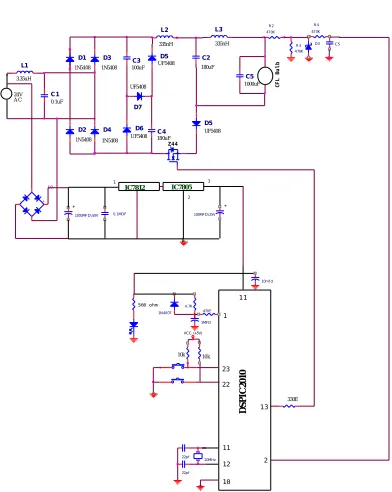
Fig 3 Circuit Diagram 1N5408 10 C5 1N5408 10k 1000MFD\ 50V Z44 D4 23 D5 1N5408 + R3 4 70K 24V A C 22p f C2 IC7805 D2 C F L B u l b 0. 1MDF 1 2 13 1N40 07 3.35uH 22 D6 R2 47 0K 335nH 3 R4 47 0K C5 335nH 11 D3 0.1uF C4 D S P IC 2 0 1 0 - + D3 2 L1 D3 100MFD\ 25V 100uF 11 UF5408 D7 180uF L2 L3 12 UF5408 180uF C1 UF5408 330E C3 1MFD 1000uF IC7812 D5 UF5408 1 4. 7K 10mf d D1 560 ohm 22p f + 20MHz 1N5408 10k VCC (+5V)
ISSN(Online): 2319-8753 ISSN (Print) : 2347-6710
I
nternational
J
ournal of
I
nnovative
R
esearch in
S
cience,
E
ngineering and
T
echnology
(An ISO 3297: 2007 Certified Organization)
Vol. 5, Issue 6, June 2016
Stage 1: t0 <t <t1. When Vg (the gate signal toM1) is high,M1 is on. iin flows from the output of the valley-fill circuit
to Lin, the resonant circuit, D4, and M1. The current (ids)flowing through M1 is simply equal to iin.
Stage 2: t1 <t <t2. M1 is still on. Meanwhile, diode D4should turn off so that iin returns to zero before the switch
turn off to minimize the MOSFET turn off switching loss. In this stage, the current flowing through M1 is equal to zero.
Stage 3: t2 <t <T s. Vg goes to zero, andM1 turns off. OnceM1 turns off, the voltage across M1 starts to increase due to
the presence of the drain-to-source capacitor of M1.It can be seen that the voltage stress across the MOSFET is a function of vrect and θ, where ω is the angular switching frequency; vrect is the voltage across the valley-fill circuit and is assumed to be constant (Vrect) within one switching cycle.
V. RESULT AND DISCUSSIONS
This paper work on harmonic interactions in nonlinear loads, especially CFLs with electronic ballast. There for a novel filter less method for harmonic suppression between groups of same loads has proposed. Experimental measurements will give to evaluate the attenuation effect between different individual lamps.
Sl.No Description Conventional method without feedback
Proposed method with feedback 01 Total Harmonics Distortion 0.7% 0.2% 02 Power consumption 15W 13.5W 03 Power Factor 0.900 0.960 04 Power loss 25% 10%
Table 1 Result
The above table shows the total harmonic distortion, Power Consumption, Power factor and Power Loss in both conventional and proposed method .In all the cases the proposed method results shows high accuracy and efficiency. Based upon the experimental results the proposed method gives the better performance.
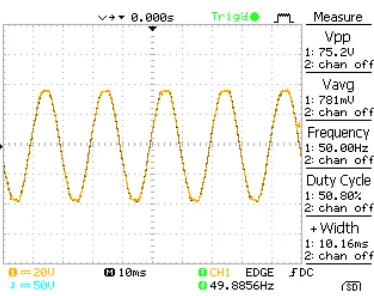
INPUT VOLTAGE
Fig 4 Input voltage to the Proposed Circuit
ISSN(Online): 2319-8753 ISSN (Print) : 2347-6710
I
nternational
J
ournal of
I
nnovative
R
esearch in
S
cience,
E
ngineering and
T
echnology
(An ISO 3297: 2007 Certified Organization)
Vol. 5, Issue 6, June 2016
GATE PULSE
Fig 5 Gate Pulse to the proposed method
The Gate Pulse also be the factor effects the Performance of the Device.The Gate pulse which is used for Switching operation to drive the MOSFET Switch .It indicate the pulse generates at 400 Hz switching frequency and it works at 27% Duty cycle. In this duty we can control voltage at constant by varying duty cycle.
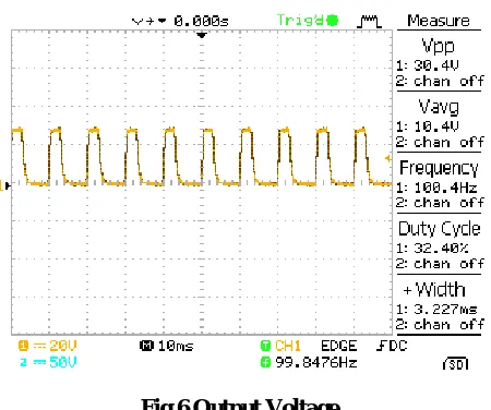
CFL OUTPUT VOLTAGE WITHOUT HARMONICS
Fig 6 Output Voltage
ISSN(Online): 2319-8753 ISSN (Print) : 2347-6710
I
nternational
J
ournal of
I
nnovative
R
esearch in
S
cience,
E
ngineering and
T
echnology
(An ISO 3297: 2007 Certified Organization)
Vol. 5, Issue 6, June 2016
VI. CONCLUSION
Single-switch has been presented in this paper for CFLs to improve the poor power factor performance in the conventional ballast design. A passive valley-fill circuit was used as the Total Harmonics distortion, Power factor improvement and reduces the power loss in the proposed ballast to form a high-power-factor single-switch ballast power circuit. To improve the lamp illumination, a simple feedback circuit to control the “valley-fill” low-frequency envelope imposed on the lamp current by adjusting the duty ratio of the switch was presented in proto type kit. The output of the above proposed method, Total harmonics distortion is minimized, Power factor has been improved and the power loss of the above circuit has been minimized.
REFERENCES
[1] G. Olivier and R. Benhaddadi, “How green are compact fluorescent lamps?” IEEE Can. Rev., pp. 21–22, Dec. 2007.
[2] J. P. de Lopes, M. F. da Silva, M. A. Dalla Costa, F. E. Bisogno, R. N. do Prado, and A. R. Seidel, “Feed forward regulation method for
self-oscillating electronic ballast for fluorescent lamps,” IEEE Trans. Ind.Electron., vol. 59, no. 4, pp. 1869–1878, Apr. 2012.
[3] R. Gules, W. Meneghette dos Santos, E. F. R. Romaneli, C. Q. Andrea,and R. C. Annunziato, “An auxiliary self-oscillating preheating system
for self-oscillating fluorescent lamp electronic ballasts,” IEEE Trans. Ind.Electron., vol. 59, no. 4, pp. 1859–1868, Apr. 2012.
[4] C. Branas, F. J. Azcondo, and R. Zane, “Power-mode control of multi phase resonant electronic ballast,” IEEE Trans. Ind. Electron., vol. 59,no.
4, pp. 1770–1778, Apr. 2012.
[5] W. M. Ng, D. Y. Lin, and S. Y. Hui, “Design of a single ultra-low loss magnetic ballast for a wide range of T5high-efficiency fluorescent
lamps,” IEEE Trans. Ind. Electron., vol. 59, no. 4, pp. 1849–1858,Apr. 2012.
[6] M. S. Perdigao, J. M. Alonso, D. G. Vaquero, and E. S. Saraiva, “Correction to “magnetically controlled electronic ballasts with isolated
output :The variable transformer solution”,” IEEE Trans. Ind. Electron., vol. 59,no. 7, p. 3042, Jul. 2012.
[7] N. R. Watson, T. L. Scott, and S. Hirsch, “Implications for distributionnetworks of high penetration of compact fluorescent lamps,” IEEE
Trans.Power Delivery, vol. 24, no. 3, pp. 1521–1528, 2009.
[8] C. S.Moo, K. H. Lee, H. L. Cheng, andW.M. Chen, “A single-stage high power-factor electronic ballast with ZVS buck-boost conversion,”
IEEETrans. Ind. Electron., vol. 56, no. 4, pp. 1136–1146, Apr. 2009.
[9] M. F. da Silva, J. Fraytag, M. E. Schlittler, T. B. Marchesan,M. A. Dalla Costa, J. M. Alonso, and R. Nederson do Prado, “Analysis and design
of a single-stage high-power-factor dimmable electronic ballast for electrode less fluorescent lamp,” IEEE Trans. Ind. Electron., vol. 60, no.
8,pp. 3081–3091, Aug. 2013.
[10] J.-C. Hsieh and J. Lin, “Novel single-stage self-oscillating electronic ballast with high power factor correction,” IEEE Trans. Ind. Electron.,vol.
58, no. 1, pp. 250–262, Jan. 2011.
[11] J. Song, J.-H. Song, I. Choy, and J.-Y. Choi, “Improving crest factor of electronic ballast-fed fluorescent lamp current using pulse frequency
modulation,” IEEE Trans. Ind. Electron., vol. 48, no. 5, pp. 1015–1024,Oct. 2001.
[12] J. C. W. Lam and P. K. Jain, “A modified valley fill electronic ballast having a current source resonant inverter with improved line-current total
harmonic distortion (THD), high power factor, and low lamp crest factor,”IEEE Trans. Ind. Electron., vol. 55, no. 3, pp. 1147–1159, Mar. 2008.
[13] Z.-R. Lee, H.-C. Hsiao, and C.-S. Lin, “Improving current crest factor of fluorescent lamp with valley-fill filter using pulse width modulation,”
inProc. IEEE 2nd Conf. ICIEA, May 2007, pp. 1686–1691.
[14] P. Tam, H. Chung, and S. Y. Hui, “Iterative behavioral modeling of charge pump based electronic ballast-fluorescent lamp system,” IEEE
Trans.Power Electron., vol. 24, no. 1, pp. 278–287, Jan. 2009.
[15] H.-J. Chiu and S.-J. Cheng, “Single-stage voltage source charge-pump electronic ballast with switched-capacitor dimmer for multiple