Closed Loop Controlled Dc-Dc Voltage
Quadrupler
Aglare Emmanuel Das
1, Krishnakumar M
2PG Student [PE], Dept. of EEE, Vidya Academy of Science & Technology, Thrissur, Kerala,India1
Assistant professor, Dept. of EEE, Vidya Academy of Science & Technology, Thrissur, Kerala,India 2
ABSTRACT: A Closed Loop Controlled DC-DC Voltage Quadrupler is proposed. The proposed topology utilizes input-parallel output-series configuration for providing a higher voltage gain without using a large duty cycle. The converter can achieve high step-up voltage gain with the reduced number of components and also reduce the voltage stress of both active switches and diodes. This allows choosing a lower voltage rating MOSFETs and diodes to reduce both switching and conduction losses. Furthermore, by the charge balance of the blocking capacitor, the converter features automatic uniform current sharing characteristics of the two interleaved phases for voltage boosting mode while excluding extra circuitry or complex control strategies. The closed-loop controlled dc-dc voltage quadrupler converter is achieved using a microcontroller; the controller is designed such that the designed output voltage is held constant for a change in the input voltage for a fixed tolerance limit. The simulations are done in Matlab Simulink.
KEYWORDS: Closed Loop Control,Comparison of with and without feedback circuit,DC-DC converter, Voltage Quadrupler, Hardware implementation.
I.INTRODUCTION
The renewable energy sources such as solar cells and fuel cells are increasingly used worldwide for electric energy generation to replace energy from fossil fuel. The output voltage generated by the sources such as photovoltaic arrays, the fuel stacks or the battery sources are very low, in the range of 12-48 V. Due to the inherent low voltage characteristic of these sources, a high step-up dc converter is essential as a prestage of the corresponding power conditioner. Boost-type architecture with a large voltage gain is required to link this voltage to an inverter the conventional boost and buck-boost converters, due to the degradation in the overall efficiency as the duty ratio approaches unity [1], cannot fulfil the application need. Furthermore, an extremely large duty ratio not only induces very large voltage spikes and increases conduction losses but it also induces severe diode reverse-recovery problem [2],
The switched capacitor-based converters proposed in [3], [4] provide solutions to improve the conversion efficiency and achieve a large voltage conversion ratio. Unfortunately, the conventional switched capacitor technique makes the switch suffer high transient current and large conduction losses. But in order to obtain an extremely high step-up conversion, many switched capacitor cells are required which increases the circuit complexity [5].
boost converter a good candidate to interface the photovoltaic systems. Another possibility to reduce the converter’s input current ripple is given by the interleaving structures. The interleaved structure can effectively increase the switching frequency and reduce the input and output ripples as well as the size of the energy storage inductors. The proposed system has a two-phase interleaved boost converter to realize a high voltage gain, maintain the advantage of an automatic current sharing capability simultaneously, high efficiency, low input current ripple, and better transient responses. And the added advantage of, the voltage stress of active switches and diodes in the proposed converter can be greatly reduced to enhance overall conversion efficiency.
II.LITERATURE SURVEY
Before the development of power electronic (PE) devices one way to convert the voltage of a DC supply to a higher voltage, for low-power applications, was to convert it to AC by using a rotating machine followed by a step-up transformer and rectifier. These were relatively inefficient and expensive procedures. With the onset of PE devices and IC’s made it economically viable to use techniques as to convert the DC power supply to high-frequency AC, with small transformer which is light, and cheap due to the high frequency to change the voltage, and rectify back to DC. Practical electronic converters use switching techniques. DC level higher or lower than the input is acquired by storing and releasing the energy to at different voltage levels commonly called switched-mode converters.The recent increase in fossil fuel cost and new regulations to reduce CO2emissions have increased the interest in renewable energy
resources in general. Fuel cells and photovoltaics (PVs) have been gaining a lot of interest as leading renewable energy technologies. A PV output voltage is a function of irradiation, which causes it to also vary. But the low variable voltage of the renewable energy technologies calls for a high-efficiency high-ratio dc–dc converter. The output voltage of a conventional boost converter to be approximately four times its applied voltage due to the practical considerations. In order to supply a high output voltage, the conventional boost converter must operate at extremely high duty cycle ratios.Large duty cycles put inefficiently small off times or lower switching frequencies.The electromagnetic interference (EMI) levels are increased due to the smaller off which causes very severe diode reverse recovery current which in turn increases EMI.And Lower switching frequency leads to greater ripple current and adds magnetic components. Moreover, an extreme duty cycle is not desirable since no room is left for control to compensate changes in a load or a line. And high power rated semiconductor devices are needed for a conventional high step-up boost converter. The drawback associated with that is the size, cost, and degradation of the overall converter efficiency. The aforementioned and related drawbacks associated with existing high step-up boost converters encourage a search for better high step-up converter topology which enables the use of a lower voltage rated Switches and diodes for increasing better efficiency by reducing the conduction as well as the switching losses.
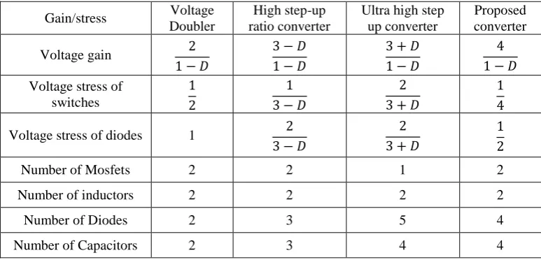
Table 1-Comparison of different converter topologies Gain/stress Voltage
Doubler
High step-up ratio converter
Ultra high step up converter
Proposed converter
Voltage gain 2
1 − 𝐷
3 − 𝐷 1 − 𝐷
3 + 𝐷 1 − 𝐷
4 1 − 𝐷
Voltage stress of switches
1 2
1 3 − 𝐷
2 3 + 𝐷
1 4
Voltage stress of diodes 1 2
3 − 𝐷
2 3 + 𝐷
1 2
Number of Mosfets 2 2 1 2
Number of inductors 2 2 2 2
Number of Diodes 2 3 5 4
The table 1 shows the comparison of four different boost converter topologies the voltage gain, component count, as well as the voltage stress across the semiconductor devices.
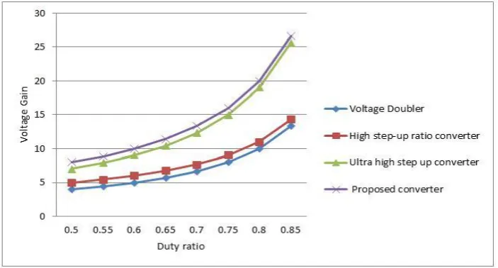
Duty ratio Voltage Doubler
High step-up ratio converter
Ultra high step up converter
Proposed converter
.50 4 5 7 8
.55 4.44 5.44 7.88 8.88
.60 5 6 9 10
.65 5.714 6.714 10.42 11.42
.70 6.66 7.66 12.33 13.33
.75 8 9 15 16
.80 10 11 19 20
.85 13.33 14.33 25.66 26.66
Table 2- Relation between duty ratio and voltage gain of different converter
The table 2 is formed from the voltage gain equations form table 1, for the same duty ratio the voltage gain of the different boost converter are calculated and tabulated.
Figure 1-Graph plotted between Voltage gain vs Duty ratio
III.METHODOLOGY
3.1-BLOCK DIAGRAM
Figure 2-Block diagram of proposed converter
The Figure 2 shows the block diagram of a closed-loop controlled dc-dc voltage quadrupler .The dc source supplies power to the voltage quadrupler topology and the output voltage is measured and compared with the reference voltage.The voltage difference between the reference voltage and actual voltage is fed back to the controller. The controller adjusts the switching pulses to make the actual voltage identical as that of the required voltage.
The block diagram with white arrows shows the existing topology [A Novel Transformer-less Adaptable VoltageQuadrupler DC Converter with Low Switch Voltage Stress]-[11].And the Black arrows shows the modification done in order to modify the existing topology to have a closed loop feedback control.
3.2-CIRCUIT DIAGRAM
Figure 4-Shows the switching pulses in different modes
There are four modes of operation for the operating principle behind the proposed converter.
Mode 1,(𝑡𝑜≤ 𝑡 ≤ 𝑡1): Switches S1 andS2 are turned ON,D1a,D1b, D2aandD2b are all OFF. Both IL1 and IL2 are increasing
to store energy in L1 andL2,respectively. The voltages across diodes D1a andD2a are clamped to capacitor voltageVCA
and VCB, respectively, and the voltages across the diodes D1b and D2b areclamped to VC2 minus VCB and VC1 minus
VCA, respectively. Also, the load power issupplied from capacitors C1 and C2.
Mode 2,(𝑡1≤ 𝑡 ≤ 𝑡2): For this operation mode, switch S1remains conducting and S2 is turned OFF. DiodesD2a andD2b
become conducting. Part of stored energy in inductorL2as well as the stored energy of CA is now released to output
capacitorC1and load. Meanwhile, part of stored energy in inductorL2 is stored in CB.
Mode 3,(𝑡2≤ 𝑡 ≤ 𝑡3): Both S1 and S2are turned ON. Similar to the first mode of operation.
Mode 4,(𝑡3≤ 𝑡 ≤ 𝑡4): For this operation mode, switch S2remains conducting andS1 is turned OFF. Diodes D1a and D1b
become conducting. The part of stored energy in inductor L1 as well as the stored energy ofCBis now released to output
capacitor C2 and load. While, part of stored energy in inductor L1 is stored in CA.
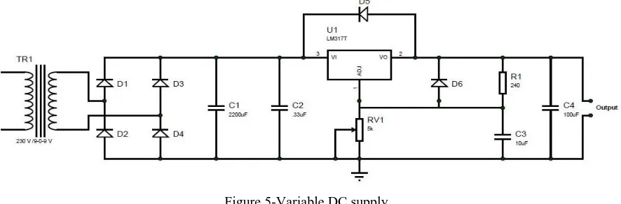
Figure 5-Variable DC supply
The figure 5 shows a variable dc supply. The circuit utilizes an LM317T a variable voltage regulator for its operation. The variable dc supply can be used to power the proposed converter. There by changing the input voltage value as desired.
𝑅2= 𝑅1
𝑉𝑜𝑢𝑡
1.25 − 1
R1 and R2 can be found from the equation .R2 is a potentiometer.
Figure 6-Optocoupler circuit
The circuit of an optocoupler (TLP350) is shown; the optocoupler helps in controlling the Mosfets without putting strain on the microcontroller. Driver IC’s are often used for high current MOSFETs and when using fast switching rates due to the MOFETs needing brief but high currents tochange state. Driver’s inputs are typically logic level. Often MOSFETS require a 1-2 A drive to achieve switching efficiently at frequencies of hundreds of kilohertz. This drive is required on a pulsed basis to quickly charge and discharge the MOSFET gate capacitances.
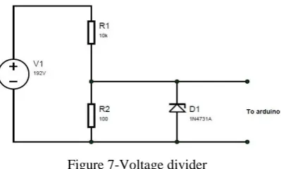
Figure 7-Voltage divider
For controlling the proposed converter Arduino UNO is selected it can generate the PWM signals necessary for controlling the Mosfets. The down side is that Arduino cannot drive the mosfet directly so optocoupler are used as an interface between the both. The output voltage is extremely high as the Arduino can only accept a maximum of 5 volts as a feedback value. So a solution to this problem is to use a voltage divider to step down the voltage to a tolerable level for the Arduino. A Zener diode is also used for protection in any case a voltage higher than the threshold value reaches the controller.
IV.DESIGN
For the proposed topology the voltage gain is given by,
𝑉𝑂
𝑉𝑖𝑛
= 4
1 − 𝐷
Design for a system of Vin = 12 V, Vout= 192 V, D = .75,
𝑃 =𝑉
2
𝑅
Taking P = 75W, R = 491.52 taken as 500,
Since we know the power and voltage the current is calculated to be
I =.3906A
The inductor current ripple peak-peak amplitude is given by
∆𝑙1, 𝑙2=
𝑉𝑖𝑛𝐷
𝑓𝑠𝐿
The value of the capacitor is given by the formula,
𝑓𝑠= 40 × 103
𝐶 = 𝐷𝑉𝑜 𝑅∆𝑉𝑜𝑓𝑠
𝐶 = 3.6 × 10⁻⁶ F
The expression for finding the value of inductor is,
𝐿 =𝑉𝑖𝑛𝐷𝑇𝑠 2∆𝐼𝑜
𝐿 = 1.125 × 10⁻⁴ H
V.SIMULATION
Figure 8-Simulation of voltage quadrupler in open loop
Figure 9-Voltage and current waveforms of without feedback topology
Figure11-Voltage and current waveforms of with feedback circuit-1
Figure13-Voltage and current waveforms with feedback circuit-2
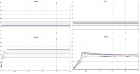
Figure 14-Input voltage & Output voltage with and without feedback
Figure15-Input voltage & Output voltage with and without feedback with transient response
Figure 15 shows the transient response of the converter as the input changes the output also changes for without feedback simulation shown on the left side and on the right side the converter is working with feedback and the output voltage is held constant for the changes in input voltage.
Input voltage
Without feedback
With feedback Loop-1
With feedback Loop-2
10 159.4 189.7 176.9
11 175.7 191 178.2
12 191.9 191.4 179.4
13 208.2 191.7 180.3
14 224.4 190.1 181.1
Table-3 Input voltage and the corresponding output voltage
Figure 16-Input voltage vs Output voltage
The figure shows the graphical representation of the Table-3 here we can see that without feedback line steadily increases and the with feedback loop-1 and 2 are fairly constant that is the outout is held constant even though the input voltage changes.
Figure-17 Flowchart of closed loop control operation
V. RESULT AND DISCUSSION
Figure 18- Switching pulses for the Mosfets
Figure 19-Shows the complete hardware of the closed loop controlled DC-DC voltage quadrupler
VI.CONCLUSION
A closed loop controlled dc-dc voltage quadrupler is designed, simulated, fabricated and tested. The circuit was designed for an input voltage of 12 volts and an output voltage of 192 volts. And for a variation in input voltage (20 % of the designed input voltage) the output is held constant. For the purpose of this project work a converter [A Novel Transformer-less Adaptable VoltageQuadrupler DC Converter with Low Switch Voltage Stress]-[11] is taken as the reference converter and modified such that it can function in a closed loop manner. The simulation of the converter in open loop and closed loop manner is done.
REFERENCES
[1] R. W. Erickson and D. Maksimovic, ”Fundamentals of Power Electronics”, 2nd ed. Norwell, MA, USA: Kluwer, 2001.
[3] F. Zhang, L. Du, F. Z. Peng, and Z. Qian, “A new design method for high power high-efficiency switched-capacitor DC-DC converters,” IEEE Trans. Power Electron., vol. 23, no. 2, pp. 832840, Mar. 2008.
[4] B. Axelrod, Y. Berkovich, and A. Ioinovici, “Switched-capacitor/ switched inductor structures for getting transformer less hybrid DC-DC PWM converters,” IEEE Trans. Circuits Syst. I, Reg. Papers, vol. 55, no. 2, pp. 687696, Mar. 2008.
[5] W. Li, X. Xiang, C. Li, W. Li, and X. He,”Interleaved high Step-Up ZVT converter with built-in transformer voltage doubler cell for distributed PV generation system,” IEEE Trans. Ind. Electron., vol. 28, no. 1, pp. 300313, Jan.2013.
[6] Y. T. Jang and M. M. Jovanovic, ”Interleaved boost converter with intrinsic voltage-doubler characteristic for universal-line PFC front end,” IEEE Trans. on Power Electron., vol. 22, no. 4, pp. 13941401, Jul. 2007.49
[7] L. S. Yang, T. J. Liang, and J. F. Chen, ”Transformer less DC-DC converters with high step-up voltage gain,” IEEE Trans. Ind. Electron., vol. 56, no. 8, pp.31443152, Aug. 2009.
[8] A. A. Fardoun and E. H. Ismail, Ultra step-up DC-DC converters with reduced switch stress, IEEE Trans. Ind. Appl., vol. 46, no. 5, pp. 2025 2034, Oct. 2010.
[9] Chitra.P and Seyezhai.R”Basic Design and Review of Two Phase and Three Phase Interleaved Boost Converter for Renewable Energy Systems” International Journal of Applied Science ,05 July 2014
[10] S. Masri, P. W. Chan ”Design and Development of DC-DC boost converter with constant output voltage” School of Electrical and Electronic Engineering,Universiti Sains Malaysia, 14300 Nibong Tebal, Seberang Prai Selatan, PulauPinang, Malaysia