ISSN (Print) : 2320 – 3765 ISSN (Online): 2278 – 8875
I
nternational
J
ournal of
A
dvanced
R
esearch in
E
lectrical,
E
lectronics and
I
nstrumentation
E
ngineering
(An ISO 3297: 2007 Certified Organization)
Vol. 4, Issue 3, March 2015
Implementation of Adder by Using
Quantum-Dot Cellular Automata Technology
T Ranjitha devi
Assistant Professor, Dept. of ECE, SVIT Engg College, ATP, India
ABSTRACT: In this paper, a novel quantum-dot cellular automata (QCA) adder design is presented that decrease the number of QCA cells compared to previously report designs. The proposed one-bit QCA adder design is based on a new algorithm that requires only three majority gates and two inverters for the QCA addition. A novel 128-bit adder designed in QCA was implemented. It achieved speed performances higher than all the existing. QCA adders, with an area requirement comparable with the cheap RCA and CFA established. The novel adder operates in the RCA fashion, but it could propagate a carry signal through a number of cascaded MGs significantly lower than conventional RCA adders. In adding together, because of the adopted basic logic and layout strategy, the number of clock cycles required for completing the explanation was limited. As transistors reduce in size more and more of them can be accommodated in a single die, thus increasing chip computational capabilities. However, transistors cannot find much smaller than their current size. The quantum-dot cellular automata approach represents one of the possible solutions in overcome this physical limit, even though the design of logic modules in QCA is not forever straightforward.
KEYWORDS: Adders, nano-computing, QCA (quantum-dot cellular automata)
I. INTRODUCTION
In this paper, a new QCA adder design is implemented that reduces the number of QCA cells when compared to existing reported designs. We demonstrate that it is possible to design a CLA QCA one-bit adder, with the same reduced hardware as the bit-serial adder, as retaining the simpler clocking scheme and parallel structure of the novel CLA approach. The proposed design is based on a new algorithm that requires only three majority gates and two inverters for the QCA addition. It is noted that the bit-serial QCA adder uses a variant of the proposed one-bit QCA adder. By connect n proposed one-bit QCA adders.
ISSN (Print) : 2320 – 3765 ISSN (Online): 2278 – 8875
I
nternational
J
ournal of
A
dvanced
R
esearch in
E
lectrical,
E
lectronics and
I
nstrumentation
E
ngineering
(An ISO 3297: 2007 Certified Organization)
Vol. 4, Issue 3, March 2015
Fig 1 Novel 2-bit basic module
An adder designed as proposed runs in the RCA fashion, but it exhibit a computational delay lower than all state-ofthe- art competitors and achieves the lowest area-delay product (ADP).
II. BACK GROUND
A. QCA Basics
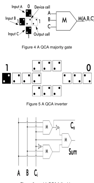
QCA is based on the interface of bi-stable QCA cells constructed from four quantum-dots. A high-level design of two polarized QCA cells is shown in Fig. 2. Each cell is constructed from four quantum dots arranged in a square pattern. The cell is charged with two electrons, which are free of charge to tunnel between adjacent dots. These electrons tend to take up antipodal sites as a result of their mutual electrostatic repulsion. Thus, there exist two equal energetically minimal arrangements of the two electrons in the QCA cell as shown in Fig. 2. These two arrangements are denoted as cell polarization P = +1 and P = -1 correspondingly. By using cell polarization P = +1 to represent logic “1” and P = -1 to represent logic “0”, binary information can be encoded.
Figure 2 QCA cells
Arrays of QCA cells can be set to perform all logic functions. This is owed to the Columbic interactions, which influences the polarization of neighboring cells. QCA designs have been proposed with potential barriers between the dots that can be controlled and used to clock QCA designs.
B. QCA Logical Devices
The fundamental QCA logic devices are the QCA wire, majority gate and inverter.
ISSN (Print) : 2320 – 3765 ISSN (Online): 2278 – 8875
I
nternational
J
ournal of
A
dvanced
R
esearch in
E
lectrical,
E
lectronics and
I
nstrumentation
E
ngineering
(An ISO 3297: 2007 Certified Organization)
Vol. 4, Issue 3, March 2015
can also be used. In this case, the propagation of the binary signal alternates between the two polarizations. Advance, there exists a so-called non-linear QCA wire, in which cells with 90-degree orientation can be placed next to one more, but off center.
Figure 3 A QCA wire (90-degree)
Majority gate and inverter: The majority gate and inverter are shown in Fig. 4 and Fig. 5 respectively. The majority gate performs a three-input logic function. Assuming the inputs are A, B and C, the logic function of the majority gate is
m(A, B,C) = A|B + B|C + A|C (1)
By fixing the polarization of one input as logic “1” or “0”, we can get an OR gate and an AND gate respectively. More complex logic circuits can then be designed from OR and AND gates.
Figure 4 A QCA majority gate
Figure 5 A QCA inverter
C. QCA Full Adders
ISSN (Print) : 2320 – 3765 ISSN (Online): 2278 – 8875
I
nternational
J
ournal of
A
dvanced
R
esearch in
E
lectrical,
E
lectronics and
I
nstrumentation
E
ngineering
(An ISO 3297: 2007 Certified Organization)
Vol. 4, Issue 3, March 2015
III. PROPOSED METHOD
A QCA is a nano-structure having as its basic cell a square four quantum dots structure charged with two free electrons able to tunnel through the dots inside the cell. Because of Coulombic repulsion, the two electrons will forever reside in opposite corners. The locations of the electrons in the cell determine two possible stable states that can be associated to the binary state 1 and 0.
Although adjacent cells interact through electrostatic forces and tend to arrange in a line their polarizations, QCA cells do not have intrinsic data flow directionality. To achieve controllable data directions, the cells inside a QCA design are partitioned into the so-called clock zones that are progressively associated to four clock signals, each phase shifted by 90°. This clock system named the zone clocking scheme, makes the QCA designs intrinsically pipelined, as each clock zone behaves like a D-latch. QCA cells are used for both logic designs and interconnections that can exploit either the coplanar cross or bridge technique. The fundamental logic gates inherently available within the QCA technology are the inverter and the MG. Given three inputs a, b, and c, the MG perform the logic function reported in (1) provided that all input cells are associated to the same clock signal clkx (with x ranging from 0 to 3), whereas the remaining cells of the MG are linked to the clock signal clkx+1
ISSN (Print) : 2320 – 3765 ISSN (Online): 2278 – 8875
I
nternational
J
ournal of
A
dvanced
R
esearch in
E
lectrical,
E
lectronics and
I
nstrumentation
E
ngineering
(An ISO 3297: 2007 Certified Organization)
Vol. 4, Issue 3, March 2015
Several designs of adders in QCA exist in literature. The RCA [11], [13] and the CFA [12] process n-bit operands by cascading n full-adders (FAs). Even although these addition circuits use different topologies of the generic FA, they include a carry-in to carry-out path consisting of one MG, and a carry-in to sum bit path contain two MGs plus one inverter. As a importance, the worst case computational paths of the n-bit RCA and the n-bit CFA consist of (n+2) MGs and one inverter. A CLA design formed by 4-bit slices was also presented. In particular, the auxiliary propagate and generate signals, namely
�� = �+ �and ��= �. �, are compute for each bit of the operands and then they are grouped four by four. Such a designed n-bit CLA has a computational path composed of 7+4×(log4�) cascade MGs and one inverter. This can be easily verified by observing that, given propagate and generate signals, to compute grouped propagate and grouped generate signals; four cascade MGs are introduced in the computational path. In addition, to calculate the carry signals, one level of the CLA logic is required for each factor of four in the operands word-length. This means that process n bit addends, log4� levels of CLA logic are required, every contributing to the computational path with four cascaded MGs. Finally, the calculation of sum bits introduces two further cascaded MGs and one inverter. The parallel-prefix BKA demonstrated exploits more efficient basic CLA logic designs. As its main
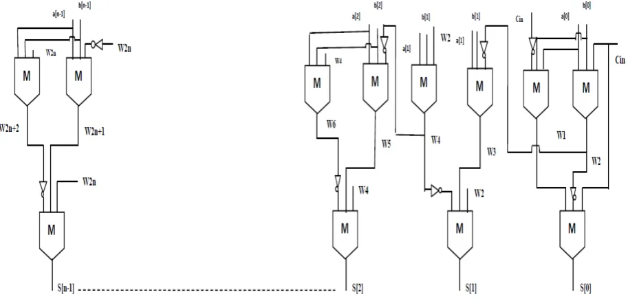
Novel 16-bit adder
ISSN (Print) : 2320 – 3765 ISSN (Online): 2278 – 8875
I
nternational
J
ournal of
A
dvanced
R
esearch in
E
lectrical,
E
lectronics and
I
nstrumentation
E
ngineering
(An ISO 3297: 2007 Certified Organization)
Vol. 4, Issue 3, March 2015
IV. NOVEL QCA ADDER
To introduce the novel design proposed for implementing ripple adders in QCA, let consider two n-bit addends A = �− , . . . , and B = �− , . . . , and suppose that for the i th bit position (with i = n − 1, . . . , 0) the auxiliary propagate and generate signals, namely ��= �+ �and
Novel 32-bit adder
Novel 64-bit adder
ISSN (Print) : 2320 – 3765 ISSN (Online): 2278 – 8875
I
nternational
J
ournal of
A
dvanced
R
esearch in
E
lectrical,
E
lectronics and
I
nstrumentation
E
ngineering
(An ISO 3297: 2007 Certified Organization)
Vol. 4, Issue 3, March 2015
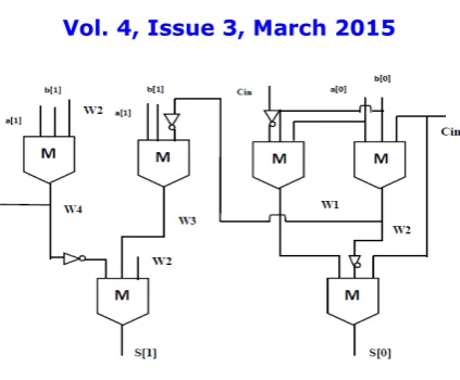
rewritten as given in (3), by exploiting Theorems 1 and 2 demonstrated. In this way, the RCA action, needed to propagate the carry � through the two subsequent bit locations, requires only one MG. Conversely, conventional circuits operating in the RCA fashion, namely the RCA and the CFA, require two cascaded MGs to perform the same operation. In other words, an RCA adder designed as proposed has a worst case path almost halved with respect to the conventional RCA and CFA. Equation (3) is exploited in the design of the novel 2-bit module shown in Figure. 1 that also shows the computation of the carry �+ = M(���� � ). The proposed n-bit adder is then implemented by cascading n/2 2-bit modules as shown in Fig. 2(a). Having assumed that the carry-in of the adder is �� = 0, the signal � is not required and the 2-bit module used at the least significant bit position is simplified.
It must be noted that the time critical addition is performed when a carry is generated at the least significant bit position and then it is propagated through the subsequent bit positions to the most significant one. In this case, the first 2-bit module computes , causal to the worst case computational path with two cascaded MGs. The subsequent 2-bit modules contribute with only one MG each, thus introducing a total number of cascaded MGs equal to (n − 2)/2. Considering that additional two MGs and one inverter are required to compute the sum bits, the worst case path of the novel adder consists of (n/2) + 3 MGs and one inverter.
V. RESULTS
The proposed addition design is implemented for several operands word lengths using the QCA Designer tool adopting the same rules and simulation settings used.
ISSN (Print) : 2320 – 3765 ISSN (Online): 2278 – 8875
I
nternational
J
ournal of
A
dvanced
R
esearch in
E
lectrical,
E
lectronics and
I
nstrumentation
E
ngineering
(An ISO 3297: 2007 Certified Organization)
Vol. 4, Issue 3, March 2015
RTL schematic
ISSN (Print) : 2320 – 3765 ISSN (Online): 2278 – 8875
I
nternational
J
ournal of
A
dvanced
R
esearch in
E
lectrical,
E
lectronics and
I
nstrumentation
E
ngineering
(An ISO 3297: 2007 Certified Organization)
Vol. 4, Issue 3, March 2015
Design summary
Simulation output
VI. CONCLUSION
ISSN (Print) : 2320 – 3765 ISSN (Online): 2278 – 8875
I
nternational
J
ournal of
A
dvanced
R
esearch in
E
lectrical,
E
lectronics and
I
nstrumentation
E
ngineering
(An ISO 3297: 2007 Certified Organization)
Vol. 4, Issue 3, March 2015
REFERENCES
[1] C. S. Lent, P. D. Tougaw, W. Porod, and G. H. Bernestein, “Quantum cellular automata,” Nanotechnology, vol. 4, no. 1, pp. 49–57, 1993. [2] M. T. Niemer and P. M. Kogge, “Problems in designing with QCAs: Layout = Timing,” Int. J. Circuit Theory Appl., vol. 29, no. 1, pp. 49–62, 2001.
[3] J. Huang and F. Lombardi, Design and Test of Digital Circuits by Quantum-Dot Cellular Automata. Norwood, MA, USA: Artech House, 2007.
[4] W. Liu, L. Lu, M. O’Neill, and E. E. Swartzlander, Jr., “Design rules for quantum-dot cellular automata,” in Proc. IEEE Int. Symp. Circuits Syst., May 2011, pp. 2361–2364.
[5] K. Kim, K. Wu, and R. Karri, “Toward designing robust QCA architectures in the presence of sneak noise paths,” in Proc. IEEE Design, Autom. Test Eur. Conf. Exhibit., Mar. 2005, pp. 1214–1219.
[6] K. Kong, Y. Shang, and R. Lu, “An optimized majority logic synthesis methology for quantum-dot cellular automata,” IEEE Trans. Nanotechnol., vol. 9, no. 2, pp. 170–183, Mar. 2010.
[7] K. Walus, G. A. Jullien, and V. S. Dimitrov, “Computer arithmetic structures for quantum cellular automata,” in Proc. Asilomar Conf. Sygnals, Syst. Comput., Nov. 2003, pp. 1435–1439.
[8] J. D. Wood and D. Tougaw, “Matrix multiplication using quantumdot cellular automata to implement conventional microelectronics,” IEEE Trans. Nanotechnol., vol. 10, no. 5, pp. 1036–1042, Sep. 2011.
[9] K. Navi, M. H. Moaiyeri, R. F. Mirzaee, O. Hashemipour, and B. M. Nezhad, “Two new low-power full adders based on majority-not gates,” Microelectron. J., vol. 40, pp. 126–130, Jan. 2009.
[10] L. Lu, W. Liu, M. O’Neill, and E. E. Swartzlander, Jr., “QCA systolic array design,” IEEE Trans. Comput., vol. 62, no. 3, pp. 548–560, Mar. 2013.
[11] H. Cho and E. E. Swartzlander, “Adder design and analyses for quantum-dot cellular automata,” IEEE Trans. Nanotechnol., vol. 6, no. 3, pp. 374–383, May 2007.
[12] H. Cho and E. E. Swartzlander, “Adder and multiplier design in quantum-dot cellular automata,” IEEE Trans. Comput., vol. 58, no. 6, pp. 721–727, Jun. 2009.
[13] V. Pudi and K. Sridharan, “Low complexity design of ripple carry and Brent–Kung adders in QCA,” IEEE Trans. Nanotechnol., vol. 11, no. 1, pp. 105–119, Jan. 2012.
[14] V. Pudi and K. Sridharan, “Efficient design of a hybrid adder in quantumdot cellular automata,” IEEE Trans. Very Large Scale Integr. (VLSI) Syst., vol. 19, no. 9, pp. 1535–1548, Sep. 2011.