Design of PWM-Based Sliding-Mode Control
of Boost Converter with Improved
Performance
TamalBiswas1, Prof. G KPanda2, Prof. P KSaha3, Prof. S Das4
PG Scholar, Dept. of EE, Jalpaiguri Government Engineering College, Jalpaiguri, West Bengal, India1
HOD and Professor, Dept of EE, JGEC, Jalpaiguri, West Bengal, India2
Professor, Dept of EE, JGEC, Jalpaiguri, West Bengal, India3
Professor, Dept of EE, JGEC, Jalpaiguri, West Bengal, India4
ABSTRACT:This letter addresses the various issues concerning the implementation of a pulse-width modulation (PWM) based sliding mode (SM) controller for boost converters.The methods of modelling the system and translation of the SM control equations for the PWM implementation are illustrated.Experimental results show that the proposed control scheme provides good voltage regulation and is suitable for common DC-DC conversion purposes. The derived controller/converter system is suitable for any changes on line voltage and parameters at input keeping load as a constant.
KEYWORDS: PID controller, Pulse Width Modulation (PWM), Sliding mode control, DC-DC boost converter,
Transfer function, MATLAB, Simulink.
I.INTRODUCTION
The switch mode DC-DC converters are some of the simplest circuit which converts power level of DC power effectively. It has wide application in modern computer, DC motor drive, power system, automotive, aircrafts etc. the commonly used control methods are pulse width modulation (PWM), voltage mode control, PWM current mode control with proportional (P), proportional integral (PI), and proportional integral derivative (PID) controller. But this control method cannot perform satisfactory under large load variation so non liner control technique is in picture. The dc-dc converters, which are non-linear and time variant system, and do not lend themselves to the application of linear control theory, can be controlled by means of sliding-mode (SM) control, Which is derived from the variable structure control system theory (VSCS). Variable structure systems are systems the physical structures of which are changed during time with respect to the structure control law. The instances at which the changing of the structure occurs are determined by the current state of the system. Due to the presence of switching action, switched-mode power supplies (SMPS) are generally variable structured systems. Therefore, SM controllers are used for controlling dc-dc converters. Though SM control compiles of various advantages, SM controlled converters suffers from switching frequency variation when the input voltage and output load are varied. Hence there are many control methods which have been developed for fixed switching frequency SM control such as fixed frequency PWM based sliding mode controllers, adaptive SM controller, digital fuzzy logic SM controller, etc. In case of adaptive control, adaptive hysteresis band is varied with parameter changes to control and fixate the switching frequency. But, these methods require more components and are unattractive for low cost voltage conversion applications.
II.LITEARTURE SURVEY
Modulation (PWM) [2]. The conventional PWM controlled power electronics circuits are modelled based on averaging technique and the system being controlled operates optimally only for a specific condition [3]-[4]. The linear controllers like P, PI, and PID do not offer a good large-signal transient (i.e. large-signal operating conditions) [4]-[5]. Therefore, research has been performed for investigating non-linear controllers. The main advantages of these controllers are their ability to react immediately to a transient condition. The different types of non-linear analog controllers are: (a) hysteretic current-mode controllers, (b) hysteretic voltage-mode/V2 controllers, (c) sliding-mode/boundary controllers. Advantages of hysteretic control approach include simplicity in design and do not require feedback loop compensation circuit. M. Castilla [6]-[7] proposed voltage-mode hysteretic controllers for synchronous buck converter used for many applications. The analysis and design of a hysteretic PWM controller with improved transient response have been proposed for buck converter in 2004.
III
.
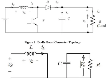
BASIC PRINCIPLESIn a boost regulator the output voltage is greater than the input voltage- the name “boost”. A boost regulator using apower MOSFET, the circuit operation can be divided into two modes. Mode 1 beings when transistor M1 switched on at t=0. The input current, which rises, flow through inductor L and transistor Q1.
Figure 1: Dc-Dc Boost Converter Topology
Figure 3: Circuit during t off
Mode2 beings when transistor M1 is switched off at t=t1. The current that was flowing through the transistor would now flow through L, C, load, and diode Dm. The inductor current falls until transistor M1 is turned on again in next cycle. The energy stored in inductor L is transferred to the load. The equivalent circuits for the modes of operation are shown in Fig:3 The waveforms for voltage and currents are shown in fig:5 For load current, assuming that the current rises or falls linearly.
Figure 4: Phase Plot for (a) ideal SM Control (b) actual SM control
The basic idea of SM control is to design first a sliding surface in state space and then the second is to design a control law direct the system state trajectory starting from any arbitrary initial state to reach the sliding surface in finite time, and finally it should come to a point where the system equilibrium state exists that is in the origin point of the phase plane. The existence, stability and hitting condition are the three factors for the stability of sliding mode control. SM control principle is graphically represented in Figure 4, where, represent the sliding surface and x1 and x2 are the voltage error variable and voltage error dynamics respectively. The sliding line (when it is a two variable SM control system in two-dimensional plane) divides the phase plane into two regions. Each region is specified with a switching state and when the trajectory arrives at the system equilibrium point, the system is considered as stable.
IV.IMPLEMENTATION OF PWM CONTROLLED BOOST CONVERTER
3.1 Dc/Dc Boost Converter Using PWM
:
Control circuit regulates output by varying on time of switch and fixing switching frequency, in pulse width modulation (PWM) Technique. Control circuit regulates output by varying switching frequency and fixing on or off time of switch, in resonant switch mode power supplies.
The main function of DC converter is power conversion and appropriate operation of semiconductor switches. DC-DC converters are generally designed for input voltage and load conditions, that is they must operate in steady state conditions only. But, practically it may not be possible due to possibility of some disturbances which causes system to deviate from nominal values. These disturbances may be due to changes in circuit parameters, source, load, disturbances in switching such as shut down and start up.
3.2 Control Principle:
Fig 4: power supply components
The fig.4 describes control principle of pulse width modulation. Power stage has two inputs: input voltage and duty cycle. Duty cycle is control input i.e. it controls the switching action of power stage and hence output. Error amplifier amplifies error and regulates output voltage.
In pulse width modulation rectangular pulse wave is used which results in the variation of the average value of the waveform. If we consider a pulse waveform f(t) with its minimum value ymin , a maximum value ymax and a duty cycle D, then the average value of the waveform can be given by the expression,
Where, ymax is 0 < t < D.T and ymin is D.T < t < T.
Therefore,
It can be simplified by putting ymin = 0 so, y =D.ymax.
Therefore, average value of signal is directly dependant on duty cycle D.
V. CONTROL TECHNIQUES FOR BOOST CONVERTER
4.1System Design: The first step to the design of an SM controller is to develop a state-space description of the converter model in terms of the desired control variables (i.e., voltage and/or current etc,). Our focus in this paper is the application of SM control to converters operating in CCM. The controller under study is a second-order proportional integral derivative (PID) SM voltage controller. Unlike most previously proposed SM voltage controllers, it takes into account an additional voltage error integral term in the control computation to reduce the steady-state dc error of the practical SM controlled system.
A second-order PID type of SM voltage controller is adopted. Fig.5 shows the schematic description of the proposed
SMVC boost converters, where C,L, and
r
L are the capacitance, inductance, and load resistance of the converters, respectively; ic,iL,andir are the capacitor, inductor, and load currents, respectively;Vref, νi, and βνo are the reference,lets consider, voltage error be X, rate of change of voltage error be Y & integral of voltage error be Z. Under continuous conduction mode, derived in can be expressed as,
Xboost=AXboost+Bu
Where, 4.2:System Modelling:
For this system, it is appropriate to have a general SM control law that adopts a switching function such as,
u= 1 when S > 0,
= 0 when S < 0,
Where S is the instantaneous state variable’s trajectory and is described as,
where, 1, 2 and 3 are representing control parameter termed as sliding coefficients.
A sliding surface can be obtained by enforcing, S = 0. Finally, the mapping of the equivalent control function onto the duty ratio control d, where
Fig 5: System modelling of sliding mode controller
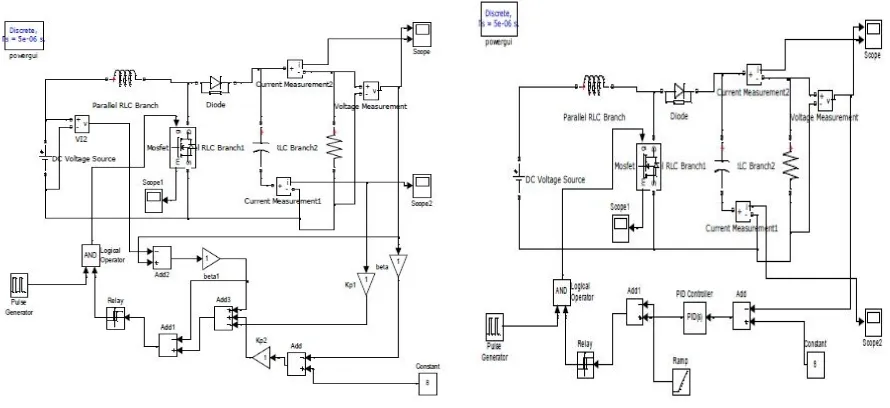
VI. SIMULINK MODEL
5.0 SIMULINK MODEL OF CONTROLLER:
Fig. 7 Simulated block diagram for boost converter using PI control
VII.SIMULATION RESULT
Fig: 8
.
Simulation result for boost converter using sliding mode controller (a) current (b) voltage.Fig: 9 Simulation result for boost converter using PI controller
VIII.CONCLUSION
IX.FUTURE WORK
Following are the areas of future study which can be considered for further research work.The proposed control method is applied on dc-dc boost converter. It can be applied to many other converter topologies. The non zero steady state error is minimized by adding PI block in the feedback control loop.The using the sliding mode control concept used for studying the behaviour of controlled dc-dc boost converter can be extended for other converter topologies. To verify the theoretical study, the proposed control scheme can be done with experimental prototype.
REFERENCES
[1] M. H. Rashid, Power Electronics: Circuits, Devices and Applications (3rd Edition), Prentice Hall, 2003.
[2] Utkin V., Guldner J., and Shi J.X., Sliding Mode Control in Electromechanical Systems. London, U.K.: Taylor and Francis, 1999.
[3] Tan S.C., Lai Y.M., Cheung M.K.H. and Tse C.K., \A Fixed-Frequency Pulse-Width-Modulation Based Quasi Sliding Mode Controller for Buck Converters," IEEETransactions on Power Electronics, vol. 20 no. 6, pp. 1379-1392, Nov. 2005.
[4] P. Mattavelli, L. Rossetto, G. Spiazzi, and P. Tenti, “General-purpose sliding-mode controller for dc/dc converter applications,” in Rec. IEEE Electron. Specialists Conf. (PESC’93), Jun. 1993, pp. 609–615.
[5] S. C. Tan, Y. M. Lai, and C. K. Tse, “Adaptive feedforward and feedback control schemes for sliding mode controlled power converters,” IEEE Trans. Power Electron., vol. 21, no. 1, pp. 182–192, Jan. 2006.
[6] H. Sira-Ramirez, “A geometric approach to pulse-width modulated control in nolinear dynamical systems,” IEEE Trans. Automat. Contr., vol.34, no. 3, pp. 184–187, Feb. 1989.
[7] R. Venkataramanan, A. Sabanoivc, and S. C´ uk, “Sliding mode control of DC-to-DC converters,” in Proc. IEEE Conf. Industrial Electronics,Control Instrumentations (IECON), 1985, pp. 251–258.
BIOGRAPHY
Tamal Biswas was born in West Bengal, India on july 19, 1988. He has received his B.Tech degree in Electrical Engineering from Birbhum Institute of Engineering and Technology,Suri, Birbhum, West Bengal in 2012. Currently he is persuing hisM.Tech degree in Power Electronics and Drives from Jalpaiguri Govt. Engineering College, Jalpaiguri, West Bengal.
Prof.Gautam Kumar Panda, Professor and Head, Department of Electrical Engineering, Department of Electrical Engineering, Jalpaiguri Government Engineering College, Jalpaiguri,WB- 735102,BE (Electrical) from J.G.E. College, Jalpaiguri, M.E.E(Electrical) Specialization: Electrical Machines & drives from JadavpurUniversity.PhD from University of North Bengal. FIE, MISTE, Certified Energy Auditor.
Prof.Pradip Kumar Saha, Professor, Jalpaiguri Government Engineering College, Jalpaiguri,WB- 735102. BE (Electrical) from B.E. College, Shibpore. M.Tech((Electrical) Specialization: Machine Drives & Power Electronics from IIT- Kharagpur.PhD from University of North Bengal. FIE, MISTE, Certified Energy Auditor.