Design of a Low-Power Low-Noise Phase Lock
Loop
Nitesh Pareek, Rahul Moud
Research Scholar, M. Tech . (VLSI), Geetanjali Institute of Technical Studies, Udaipur, Rajasthan, India
Assistant Professor, Department of EC, Geetanjali Institute of Technical Studies, Udaipur, Rajasthan, India
ABSTRACT: A phase lock loop is a closed-loop system that causes one system to track with another. More precisely, a PLL can be perceived as a circuit synchronizing an output signal with a reference or input signal in frequency as well as phase. High-performance phase lock loops are widely used within a digital system for clock generation, timing recovery, and to efficiently sequence operations and synchronize between function units and ICs As the digital system grows the role of phase lock loop increases. Achieving low jitter and phase noise in phase lock loop with less area and power consumption is challenging. The present research relates to characterization and redesign of individual blocks of Phase lock loop (PLL) to improve its characteristics. More specifically redesigning of individual blocks like: Phase Frequency Detector to reduce area and static phase error, Voltage to Current converter to linearly increase the current input to the current controlled oscillator, Current Controlled Oscillator to reduce phase noise, amplitude distortion, area and power consumption. We also introduce an additional feedback loop to increase the gain of the charge pump in a manner that linearizes the overall loop gain over wide bandwidth. The Results are substantial improvements in the PLL characteristics such as low jitter, phase noise, area and power consumption.
I. INTRODUCTION
Phase locked loops (PLLs) are essential building blocks for almost all integrated Circuits. A Phase-locked loop (PLL) is the most widely used mixed-signal circuit block in a system-on-chip. Advancements in CMOS process technology have enabled circuits to be realized at low power and high performance. But, along with these advantages there exist a number of undesirable traits, such as a high degree of process and temperature variability, high leakage, and low dynamic range due to low supply voltage. This paper discusses the impact of these effects in designing Phase-Locked Loops in Nanometer CMOS.
Continuous scaling poses several design challenges for future high performance architectures. Systematic and random variations in process, supply voltage and temperature (PVT) have become a major challenge to future high performance architecture designs. Two main contributors to on chip variability arise from changes in process parameters and changes in operating temperatures.
VCO is the most important block of the PLL. Since area is dominated by the size of the inductor, LC oscillator does not scale well with technology. Therefore, we propose ring oscillator in our PLL design. Section (2) discusses the issues that are related to process and temperature compensated VCO. The free-running frequency of a ring oscillator is very sensitive to process, voltage and temperature (PVT). Process and Temperature compensation techniques for minimizing the variation of the free-running frequency of an oscillator are considered.
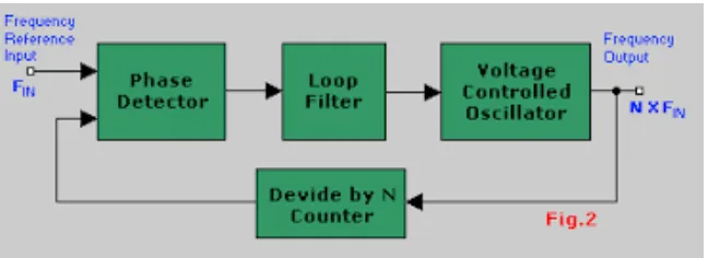
II. BASIC PLL CIRCUIT
A PLL is a feedback system that compares the output phase with the input phase. The comparison is performed by a „phase comparator‟ or „phase detector‟. The basic elements of a Phase locked Loop (PLL) are a Phase detector (PD), Low Pass Filter (LPF) and a voltage controlled oscillator (VCO) in a feedback loop.
The role of Phase detector is to compare the phase of Vout and Vin and then generating an error. Thus PD detects a phase error between the reference signal and the output signal of PLL. And the error detection range can be extended with PFD. The input phase errors are detected by Phase-Detector (PD) or Phase - Frequency Detector (PFD). These errors (phase or frequency errors) are converted into current or voltage to control the output frequency of Voltage Controlled Oscillator (VCO) by charge pump in a charge - pump PLL. According to that error, VCO frequency varies until the phases are aligned, i.e. the loop is locked. The phase detector (PD) output, VPD, consists of a high-frequency components (undesirable), dc component (desirable) and the control voltage of the oscillator must remain quiet in the steady state, i.e. the PD output must be filtered. A Low pass filter is interpose between the PD and The VCO which is used to suppress the high-frequency components of the Phase Detector (PD) output and presenting the dc level to the oscillator.
Fig. 1 shows the basic block diagram of PLL.
Fig.1 Basic block diagram of PLL
The loop is said to be locked if ϕout - ϕin =0 (Δϕ=0) does not change with time. (d ϕout /dt) – (dϕin /dt) = 0
and hence ϕout = ϕin
Basic Charge pump circuit:
Fig 2 Basic charge pump circuit diagram
The circuit of charge pump is shown in Fig. 3. When the UP signal is high (“1”), the switch M1 is „ON‟ and Cp is charged by the upper current source I1. When the DN signal is high, the switch M2 is „ON‟ and Cp is discharged through the lower current source I2. If both of the signals UP and DN are low (“0”), then M1 and M2 are both off at node P and Vc holds the original voltage.
Fig.3 The simple model of the conventional charge pump circuit.
4. Undesirable spurious tones and phase noise(Jitter) in the output signal of the VCO.
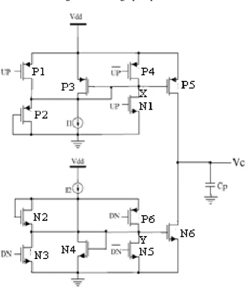
Improved charge pump circuit to overcome the above problems which uses the op-amp circuit as feedback to hold the voltage.
Fig.4 Improved charge pump
This improved Charge pump gives
1. Improved Performance
2. Improved Output Voltage
3. Reduced Complexity
4. Less Power Consumption
Fig.5 New charge pump circuit
Fig 5 : New chage ump cicuit design
III.DESIGN OF PLL Design of sense amplifier
As previously discussed in chapter about various sense amplifier, it is found that some sense amplifier consume less power but with more delay than other consume slightly more power but speed (with less delay) is relatively large. In this dissertation I propose a new sensing scheme which has less delay, more sensitivity than previously discussed with less power consumption. This chapter divided in to four parts.
Current latch sense amplifier
Latch operation
The Sizing Consideration
Body-biased controlled Current latch sense amplifier
These sense amplifiers made using with the help of tanner tool V13.1
Current Latch Sense Amplifier (CLSA)
Current Latch Sense Amplifier is based on voltage mode sense amplifier. It is also classified in differential type voltage sense amplifier. In this amplifier two cross-coupled inverters are used which give positive feedback as in latch type sense amplifier. But here the bit line is isolated from its output by using extra two NMOS transistors. So it has very high input impedance. The CLSA
Circuit Configuration
It consists of 5 NMOS and 4 PMOS transistors namely MN1, MN2, MN3, MN4, and MN5.
Fig 6. Current Latch Sense Amplifier (CLSA)
MN1, MP1, MN2 and MP2 make two inverters connected in cross coupled manner give positive feedback in current. MN3 and MN4 are used to couple bit line to CLSA amplifier.MP3 and MP4 are pre charge transistors. The capacitor C represents the column capacitance of bit lines for felling of SRAM in circuit. The sense amplifier has following ports namely Vsae , vout, voutb, bl, blb. The bl and blb are column bit lines of SRAM. The signals are given to the V sea which control the pre charge and enable CLSA. The amplified output is taken from Vout node and complimentary output at Voutb node.
Current Latch Sense Amplifier (CLSA)
In this section I show the simulation results of current Latch Sense Amplifier (CLSA). The simulation time is taken for CLSA amplifier is 60 neno seconds. The simulation waveform of the CLSA is shown in figure 5.7. Figure 5.7 shows
the simulation waveform of the CLSA at VDD =5Volt. Vsae given in pulses of 0.5 duty cycle with time period of 10n
second both rise and fall time is 1n seconds. Similarly bit input to V bl is in bit form and in sequence of 10101 and
Fig 7. Simulation waveform of current latch sense amplifier for bit voltage
IV. CONCLUSION
In this paper temperature process compensated VCO with low power additional based ring oscillator and zero dead zone PFD for high performance PLL has been presented. The design is implemented in 180 nm CMOS technology. The circuits are simulated on tanner tool with GPDK 180nm CMOS technology. The simulation results show that it operates well at high frequency of 1.25GHz with power supply voltage of 1.8V. The PFD designed has nearly zero dead zone.
REFERENCES
1.Kadaba R. Lakshmikumar, “Analog PLL Design With Ring Oscillators at Low –Gigahertz Frequencies in Nanometer CMOS: Challenges andSolutions” IEEE Circuits and Systems-II, vol 56,no 5,pp 389-393, May 2009.
2. Chu-Lung Hsu,Yiting Lai, Shu-Wei Wang ,“Built –in-Self –Test for Phase Locked Loops,” IEEE In tumentation& Measurement, vol 54,no 3, pp996-1002, June 2005.
3. Won Hyo LEE, Sung Dae LEE, Jun-Dung CHO,”A High Speed , Low Power Phase Frequency Detector and Charge Pump circuits for HighFrequency Phase Locked Loops” IEICE Trans Fundamentals , vol E82-A, no 11, pp 2514-2519, November 1999.
4.A. Hajimiri, S. Limotyrakis, and T. Lee, “Jitter and phase noise in ring oscillators,” IEEE J. Solid-State Circuits, vol. 34, no. 6, pp. 790– 804,Jun.1999
5.Miranda J. Ha, “A Low-Power, High-Bandwidth LDO Voltage Regulator with No External Capacitor”, S.B. EE, M.I.T., 2007.
6.K. Lakshmikumar, V. Mukundagiri, and S. Gierkink, “A process and temperature Compensated two-stage ring oscillator,” in IEEE CustomIntegr.Circuits Conf., Sep. 2007, pp. 691–694.
7. B. Razavi, Design of Analog CMOS Integrated Circuits McGraw-Hill, 2001.
8.Kiat-Seng Yeo, Samir S .Rofail, Wang –Ling Goh , CMOS/ BiCMOS ULSI Low Voltage, Low Power Pearson Education, 2002.