Zero APT Technique for Evaluation of
RESTORING Unbalanced Voltages
Kirti Jawalbankar1, K.Chandra Obula Reddy2
M.E Student, Department of Electrical Engineering, MSS's CET, BAMU University, Jalna,
Maharashtra, India1
Asst. Professor, Department of Electrical Engineering, MSS's CET, BAMU University, Jalna,
Maharashtra, India2
ABSTRACT: Recently in Electrical power systems for dynamically coping with a range of voltage variations, Dynamic Voltage Restorers (DVRs) have been considered as most up-to-date series compensators. Their fast Response is the main advantage of DVRs, which can fulfil all most of requirements for sensitive loads. to enhance the abilities of DVRs Both the magnitude and phase displacement angle of the synthesized DVR voltage are precisely adjusted to achieve lower power utilization to maintain acceptable voltages and last longer during compensation.. The real and reactive powers are calculated in real time in the tracking loop to achieve better conditions. This technique results in less energy being taken out of the dc-link capacitor, resulting in smaller size requirements.
KEYWORDS: Zero APT (Zero Active Power Tracking), DVR, Real power, Reactive Power, Compensation, power Quality.
I. INTRODUCTION
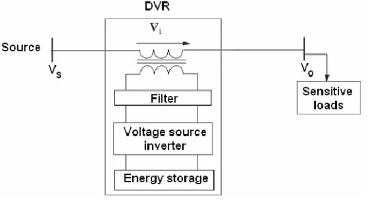
Fig 1 Schematic diagram of a typical DVR
II. CHARACTERISTICS OF VOLTAGE SAG
Voltage sag is characterized in terms of the following parameters, 1. Magnitude of sag
2. Duration of sag 3. Phase-angle jump. 4. Point on a wave
A. Magnitude of sag
Generally to characterize the sag magnitude is through the lowest per unit RMS remaining voltage during the event of sag . It means a deep sag is the sag with a low magnitude and shallow sag has a large magnitude.
Fig.2. Magnitude of voltage sag
B. Duration of sag
The duration of sag is mainly determined by the fault-clearing time. For fast clearing of the fault, duration of sag will be less and vice-versa. The duration of a sag in various standards is defined in the range from 0.5 cycle to one minute. It should be noted that the voltage reduction events shorter than 0.5 cycles influence the sensitivity of some equipment measurement and others are deliberate, using specifications that anticipate your paper as one part of the entire proceedings,
C. Phase-angle jump
The Phase-angle jump manifests itself as a shift in zero crossing of the instantaneous voltage .In three phase faults Phase-angle jumps are due to a difference in the X/R ratio between the source and the feeder. Most of the equipment are not affected by Phase-angle jumps but power electronic converters using phase angle information for their switching may be affected.
D. Point on wave
To obtain exact value for the sag duration information of “start” and “ending” of the sag is necessary. For this one needs to find the “point-on-wave of sag initiation” and the “point-on-wave of voltage recovery”. Both require more advanced analysis techniques, which are still under development.
Solutions to Power Quality Problems
III. DETECTION TECHNIQUE OF VOLTAGE SAG
A. Voltage sag detection method
The proposed method for the detection of voltage sags is based on the alfa/beta vector magnitude Vαβ , which has a
constant nominal value when no voltage sags occur. Therefore, it is only necessary to apply the Concordia transformation, and to calculate the alfa/beta vector magnitude to be able, by comparison with the nominal value, to detect symmetrical or asymmetrical voltage sags.
= 1 −0.5 −0.5
0 0.866 −0.866 eq(1)
In the Concordia transformation, the subscripts a, b and c denote the source phase voltages.
= + eq(2)
This method is complemented with a PLL to obtain constant amplitude sinusoidal Alfa/beta reference voltages Vrefα,
Vrefβ
B. Voltage reference generation
The dc/ac converter should control the transformer voltages in order to compensate for any disturbance affecting the load voltage. The voltage reference signals for the sliding mode controller are obtained in the alfa/beta reference frame, as seen in Fig.
Fig.3.Principle of the voltage reference frame
The choice of the voltage injection strategy for sags and swells mitigation is directly related to the energy storage system dimensioning strategy and directly influences the amount of stored energy, the choice of its tapping from the mains, and the allowable minimum DC voltage on the DC link . The injected voltage can be in phase or may have a phase shift with respect to the mains voltage during the voltage sag. As the injected voltage is phase shifted with respect to the mains voltage from zero to 90° degrees, the required stored energy varies from the maximum to its minimum value. If the injected voltage is kept with a 90° shift from the load current, it is possible to replenish load voltages without the need of active power injection. In this case the minimum allowable DC link voltage amplitude and the inverter apparent power increase . In this DVR prototype, the energy is stored in a capacitor bank which is charged by means of a bridge rectifier connected to the mains . The dimensioning criteria is based on injection in phase with respect to the mains voltage.
The Proposed Compensation Technique
The goal of zero active power tracking for enhancing DVR-based compensation is to make the most of the utilizable energy (1WDC) that is stored in the DC-link capacitor. This limited energy can be calculated as in (7); due to technical limitations, not all the stored energy can be utilized. The minimum DC-side voltage (VDCmin) must be at a level that can still provide the converter with proper operation. Anything lower than this level will result in the converter not producing the demanded AC voltage. In practice, this value can be dened as in (8). In addition, by the principle of DC-to-AC power conversion, the maximum DC voltage (VDCmax) at the DC-link should increase proportionally to the AC-side voltage (VDVR) required for every instant active compensating actions. According to these two equations, the compensation period (TC) can be given as in (9), which shows that more utilizable energy yields longer active compensation for the DVR to address sags. Obviously, less real power utilized by the DC-link capacitor means that the DVR can also last for a considerable period and overcome more of the voltage sag.
ΔWdc = C − eq(3)
≥ √2VDVR eq(4)
TC = Δ eq(5)
Therefore, in order to gain more from the DVR, the idea proposed here is to achieve a condition where the compensation process requires the least real power from the DC-link capacitor.
A. Zero Active Power Tracking
Fig.6. Zero active power tracking compensation.
The illustration in Fig. 4 also shows that the DVR voltage phasor is a stretchable one, as required, representing the compensation voltage added to the sag voltage. Its magnitude is adjusted related to the calculation of (10), and its displacement angle α is set according to (11). An angular displacement indicates the load characteristic, which can be determined directly using (12), relating to the load real power. Similar to the angle displacement, it is also tied to the resulting voltage. Therefore, adjusting the DVR voltage will result in both and being changed. By this technique, the resulting load voltage phasor may or may not be returned to the pre-sag level; some degrees displacement must be observed. The tracking process starts with the control of the converter output to provide the corresponding voltage, which must be varied to meet the targets. The magnitude and phase are increased progressively until reaching a value that results in a relatively acceptable power. Two possible targets are set as the preferred tracking boundaries. In case 1, the ideal zero active power (PDVR = 0) is achieved, while the load is still supported by some of the system reactive power. In this case, the load current lags behind the grid voltage (the sag voltage, VSag). In case 2, the minimum active power is achieved (as it cannot achieve zero active power), whenever all of the load reactive power is completely supported by the DVR and no longer supported by the system. At that point the load current appears to advance in leading the voltage sag, which indicates that the DVR not only supplies to the load side but also begins supplying reactive power back to the grid side. The increase in the phase angle α should be stopped immediately. If not, high power loss will degrade the DVR performance. Reconsidering the phasors of voltage and current shown in Fig. 4, it can be concluded that the normal and light voltage sags could possibly result in case (1) - the compensation eventually results in the zero reactive power condition. If the voltage sag is deep in a severe example, the compensation could result in the minimum power case 2. The effectiveness of this compensation process is directly reliant on a proper control system that assists the entire tracking process in order to achieve the mathematical targets detailed in the following.
| |= −2 cos (− + +Ø) + eq(6)
α= (( )) ( (ØØ)) eq(7)
γ= Ø− eq(8)
= cos( − ) = 0 eq(9)
= sin( − ) eq(10)
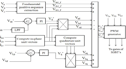
IV. CONTROL OF SELF SUPPORTED DVR
The control algorithm for self supported DVR is based on the principle of unit vectors and instantaneous symmetrical component theory for fundamental voltage extraction. The block diagram of the control system is shown in fig. Voltage sag, swell and harmonics can be compensated using this technique. The voltages at PCC (Vabc), load currents (IL), load voltages (VL) and DC voltage (VDC) are sensed for deriving the Insulated Gate Bipolar Transistor (IGBT) gate signals. The reference load voltage (VL *) is derived as image
Fig 7.Control block diagram of self supported DVR
Where VLa= Vta1- Vad+ Vaq is the reference load voltage of phase A in abc frame. Vta1 is the fundamental positive sequence voltage. Vad corresponds to required active voltage component of phase A for self supporting DC bus. Vaq is the required reactive voltage component for voltage regulation at load terminal. Reference load voltage of the remaining phases can be determined similarly. The active and reactive components of the voltage to be injected by the DVR are estimated using two PI controllers. In phase unit vectors are derived using samples of load current as, Two Proportional Integral (PI) controllers are used for regulating the DC bus voltage and the load voltage to their reference values. The reference load voltage and sensed load voltages are fed to the PWM controller for generating the gate pulses for the converter switches.
Voltage Injection Methods of DVR
Voltage injection or compensation methods by means of a DVR depend upon the limiting factors such as DVR power ratings, various conditions of load and different types of voltage sags. Some loads are sensitive towards phase angle jump and some are sensitive towards change in magnitude and others are tolerant to these. Voltage injection or compensation methods by means of a DVR depend upon the limiting factors such as DVR power ratings, various conditions of load, and different types of voltage sags. Some loads are sensitive towards phase angel jump and some are sensitive towards change in magnitude and others are tolerant to these. Therefore the control strategies depend upon the type of load characteristics.
Equations Related to DVR
The system impedance ZTH depends on the fault level of the load bus. When the system Voltage (VTH) drops, the DVR injects a series voltage VDVR through the injection transformer so that the desired load voltage magnitude VL can be maintained. The series injected voltage of the DVR can be written as
VDVR= VL + ZTHIL - VTH eq(11) Where
VL: The desired load voltage magnitude ZTH: The load impedance.
The load current IL is given by,
I = eq(12)
When VL is considered as a reference equation can be rewritten as,
VDVR 0 = VL 0 + Z TH (β –θ)- VTH δ eq(13)
β, δ are angles of ZTH, VTH, VDVR respectively and θ is Load power angle
θ = tan-1 (θ ) eq(14)
The complex power injection of the DVR can be written as,
SDVR = VDVR IL* eq(15)
It requires the injection of only reactive power and the DVR itself is capable of generating the reactive power.
V.EXPERIMENTALRESULTS
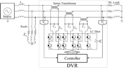
The corresponding system for verification of the proposed Compensation technique was modeled in MatLab/Simulink/PowerSys for comparison with the traditional technique, as shown in the schematically simplified diagram in Fig. 9. The main components in this system are full-bridge power converters with LC filters and DC-link capacitor (C) included, three insertion transformers used as coupling devices series connected between a three-phase power supply and a lagging power factor load, and the control that monitors the system voltage (VPCC), load voltage (VL) and current (IL), as mentioned previously.
Fig.8. .Circuit diagram model for simulation using MatLab/Simulink.
TABLE 1. Parameter ratings for simulations and experiments.
Quantity Value
VS 380V
LOAD 2.33KVA,0.45 lagging DC link Capacitor 3.3mF
LC Filter 1mH,20μF
Zf 0.43ῼ 1mH
Output signals from the control (G1-G12) were used for further gating of all the IGBTs in order to have the synthesized compensation voltage at the insertion transformer terminals, according to the technique employed. In comparison to this simulation, all the model's parameters were established relative to the overall test rig availability for the experimental tests and were scaled to available laboratory ratings. As shown in Table 1, a three-phase programmable supply of up to 380 V AC was used as the system source voltage (VS). The simulations were then conducted comparatively, as described in subsections A and B.
A. The Proposed Compensation
In order to extend the compensation as described in the previous sections, the proposed technique of zero-real power tracking was implemented with the same system mentioned in subsection A instead of the in-phase technique. The same simulation procedures were conducted, and the results were captured, as shown in Figs. 9-11. It is clear that different results were seen. The middle trace in Fig. 10 shows that by this technique, the DVR can certainly cover the entire voltage sag period, from the beginning at the time t D 0.4 s to the end at time tD0.9 s. The associated Quadrature voltages of both the DVR output and load point illustrated in Fig. 9 were increased and given the relevant voltages level led back to the desired value, as expected. It can be seen that the resulting three phase load voltage (the bottom waveform of Fig. 8) remained constant during the demand and after the sag period. The bottom trace of Fig. 10 shows that the load was therefore fed with its rating power even during the deep sag period, which was a promising result. According to this technique, much lower real power was drawn from the DC-link capacitor, which resulted in relatively less energy being output for the instant compensation. Therefore, the decrease in DC-side voltage at the DC-link was not considerable, as seen in Fig. 11, compared with in-phase compensation illustrated in Fig. 9. Only a 50 V drop is seen, compared to 250Vfor the in-phase technique. These numbers
Fig 9.The overall three-phase voltage signals during zero-real power tracking compensation
Fig 11.The DVR DC-side voltage (VDC) during zero-real power tracking compensation simply that a considerable amount of energy remained for Possible further compensation.
VI.CONCLUSION
It is clear from both the simulation and experimental results illustrated in this paper that the proposed Zero-real power tracking technique applied to DVR-based compensation can result in superior performance compared to the traditional in-phase technique. The experimental test results match those proposed using simulation, although some discrepancies due to the imperfect nature of the test circuit components were seen. With the traditional in-phase technique, the compensation was performed and depended on the real power injected to the system. Then, more of the energy stored in the DC-link capacitor was utilized quickly, reaching its limitation within a shorter period. The compensation was eventually forced to stop before the entire voltage sag period was finished. When the compensation was conducted using the proposed technique, less energy was used for the converter basic switching process. The clear advantage in terms of the voltage level at the DC-link capacitor indicates that with the proposed technique, more energy remains in the DVR (67% to 14% in the traditional in-phase technique), which guarantees the correct compensating voltage will be provided for longer periods of compensation. With this technique, none (or less) of the real power will be transferred to the system, which provides more for the DVR to cover a wider range of voltage sags, adding more flexible adaptive control to the solution of sag voltage disturbances.
ACKNOWLEDGEMENT
I am greatly indebted forever to my guide, to my HOD and all teaching and Non teaching staff those who support directly and indirectly to complete my project in time. I sincerely thank to my Principal for their continuous encouragement and active interest in my progress that they gave throughout the work. I am grateful to Have my Masters degree (EPS) from Mathshyodhsri shikshan sanstha’s collage of engineering and technology. JALNA, MAHARASTRA.
REFERENCES
1. M. Bollen, Understanding Power Quality Problems, Voltage Sags and Interruptions. New York, NY, USA: IEEE Press, 1999.
2. J. Roldán-Pérez, A. Garcí-Cerrada, J. L. Zamora-Macho, P. Roncero_Sánchez, and E. Acha, ``Troubleshooting a digital repetitive controller for a versatile dynamic voltage restorer,'' Int. J. Elect. Power Energy Syst., vol. 57, pp. 105_115, May 2014.
3. P. Kanjiya, B. Singh, A. Chandra, and K. Al-Haddad, ```SRF theory revisited' to control self-supported dynamic voltage restorer (DVR) for unbalanced and nonlinear loads,'' IEEE Trans. Ind. Appl., vol. 49, no. 5, pp. 2330_2340, Sep. 2013.
4. S. R. Naidu and D. A. Fernandes, ``Dynamic voltage restorer based on a four-leg voltage source converter,'' IET Generat., Transmiss. Distrib., vol. 3, no. 5, pp. 437_447, May 2009.
5. T. Jimichi, H. Fujita, and H. Akagi, ``A dynamic voltage restorer equipped with a high-frequency isolated DC.DC converter,'' IEEE Trans. Ind. Appl., vol. 47, no. 1, pp. 169_175, Jan. 2011.
7. P. Roncero-Sanchez, E. Acha, J. E. Ortega-Calderon, V. Feliu, and A. Garcia-Cerrada, ``A versatile control scheme for a dynamic voltage restorer for power-quality improvement,'' IEEE Trans. Power Del., vol. 24, no. 1, pp. 277_284, Jan. 2009.
8. R. Gupta, A. Ghosh, and A. Joshi, ``Performance comparison of VSC-based shunt and series compensators used for load voltage control in distribution systems,'' IEEE Trans. Power Del., vol. 26, no. 1, pp. 268_278, Jan. 2011.
9. J. G. Nielsen and F. Blaabjerg, ``A detailed comparison of system topologies for dynamic voltage restorers,'' IEEE Trans. Ind. Appl., vol. 41, no. 5, pp. 1272_1280, Sep./Oct. 2005.
10. Wessels, F. Gebhardt, and F. W. Fuchs, ``Fault ride-through of a DFIG wind turbine using a dynamic voltage restorer during symmetrical and asymmetrical grid faults,'' IEEE Trans. Power Electron., vol. 26, no. 3, pp. 807_815, Mar. 2011.
11. Y. W. Li, D. M. Vilathgamuwa, F. Blaabjerg, and P. C. Loh, ``A robust control scheme for medium-voltage-level DVR implementation,'' IEEE Trans. Ind. Electron., vol. 54, no. 4, pp. 2249_2261, Aug. 2007.
12. H. K. Al-Hadidi, A. M. Gole, and D. A. Jacobson, ``A novel con_guration for a cascade inverter-based dynamic voltage restorer with reduced energy storage requirements,'' IEEE Trans. Power Del., vol. 23, no. 2, pp. 881_888, Apr. 2008.
13. H. K. Al-Hadidi, A. M. Gole, and D. A. Jacobson, ``Minimum power operation of cascade inverter-based dynamic voltage restorer,'' IEEE Trans. Power Del., vol. 23, no. 2, pp. 889_898, Apr. 2008.
14. T. Jimichi, H. Fujita, and H. Akagi, ``Design and experimentation of a dynamic voltage restorer capable of signi_cantly reducing an energystorage element,'' IEEE Trans. Ind. Appl., vol. 44, no. 3, pp. 817_825, May 2008.
15. S. Jothibasu and M. K. Mishra, ``A control scheme for storageless DVR based on characterization of voltage sags,'' IEEE Trans. Power Del., vol. 29, no. 5, pp. 2261_2269, Oct. 2014.
BIOGRAPHY
K.chandra obula Reddy2: He was received B.tech degree from SVCET chitthur (JNTU) in 2009 and M.tech from TOCE Belgaum in 2012. and presently working as Asst.Professor, Electrical Engineering Department, MSS's CET, BAMU university, Jalna, Maharastra-431203