An Approach to Design a New
Multifunctional Reversible Logic Gate
(MRLG)
Vinay Kumar, Divya Dhawan
PG Student, Department of ECE, PEC University of Technology, Chandigarh, India
Asst. Professor, Department of ECE, PEC University of Technology, Chandigarh, India
ABSTRACT: The problem with Conventional digital circuits is the substantial energy these loss during operation. Therefore these suffer from loss of information bits hence the information itself. So a need for energy minimization was felt not just from efficiency point of view but for the proper functioning of circuit and Reversible circuits have fulfilled this need the best in the domain of digital systems. In this paper we have demonstrated functioning of a New Multifunctional Reversible Logic Gate (MRLG). The proposed MRLG gate is fully reversible and designed with CMOS and pass transistor (PT) logic design technique which has many inherent benefits such as: low power consumption, small delay and area. We have also presented a 16-bit binary logic operation circuit which is designed using a single MRLG unit.
KEY WORDS: Reversible logic, CMOS and pass transistor (PT) logic, MRLG gate, 16 -Boolean logical function,
I. INTRODUCTION
Moore’s law, that has only outperformed itself in the past, states that, the number of the transistor fabricated in an IC doubles in a period of a year and a half, so does the heat generation arising from the increasing chip density. Hence In the past years the incentives of Reversible logic have become increasingly motivating. During the operation conventional gates dissipate heat on losing a bit. In 1973 C.H Bennett [1], a physicist, demonstrated that when a circuit is designed with reversible logic no energy dissipation takes place. A circuit is reversible if one can recover input data from the output data which means the circuit information is lossless. The general considerations of bijectivity is imposed on the design of reversible logic, which means that the circuit design should have equal number of output and input and one to one mapping. This eliminates the loss of information that is main reason for power dissipation. The unused outputs of reversible gate are called Garbage output similarly Redundant Inputs to reversible gate are called Garbage inputs. Complexity and Performance of reversible circuits/ gate are defined by the following parameters
Number of logic gates
Number of garbage and constant inputs
Number of Garbage outputs.
Fan-out is restricted in reversible logic gate. The fan- out of each gate is equal to one. If more fan out are required then use a copying gate.
II. RELATED WORK
Various similar implementation of logic gates have been addressed in [1-14], the classification is defined in terms of its size and functionality. The 1x1 reversible gate is NOT. The 2x2 reversible gate is Feynman. The 3x3 reversible gates are Fredkin, Toffoli, Peres, TR gate, new gate, PRT-1 and PRT-2 and the 4x4 gate includes MKG, TSG and DKG. In Table 1 we have described the logic functionality and a brief description of various gates.
Table 1: Existing Reversible Logic Gates
Reversible Gate (Existing)
Gate
Size Input and output Functionality Logic Discription
Quantum cost
Feynman
1985 [ 5] 2x2
Input A, B Output P =A and
Q = A ⊕ B
Buffer, Ex-OR
Output Q = A’ , when input A=1 = Buffer, otherwise
1
Fredkin
1982 [6 ] 3x3
Input A, B, C Output P=A, Q=A’B⊕AC and
R=A’C’⊕ AB) C- Swap gate
Output Q = C and R = B when input A = 1. Otherwise Q = B and R
= C’.
5
Toffoli 1980 [ 16]
3x3
Input A, B, C Output P=A, Q=B and
R=AB⊕ C
Buffer, C-Controlled gate
R = C’ , When A =1 and B = 1 = Buffer, otherwise
5
Peres
1985[14 ] 3x3
Input A, B, C Output P=A, Q= A⊕ B and
R=A⊕ BC
Controlled NOT, CC-NOT, Copying
gate
Q = B’, When A=1 R= C’, When A=1 and
B=1.
4
TR 2011 [7 ]
3x3
Input A, B, C Output P=AQ= A⊕ B, R=AB’⊕ C
NAND, Buffer
R = A NAND B, when B = inverted
input
6
New 2002 [2]
3x3
Input A, B, C Output P=A, Q= AB⊕ C,
R=A’C’⊕ B’
Buffer, AND, Ex-OR
R= A’ Ex-OR B’, When C=0 Else Q= A AND B
7
PRT-I 2011[15 ]
3x3
Input A, B, C
Output P=AB⊕B’C,Q=A⊕ B⊕
C and R=AB’⊕ BC
OR , AND, Ex-OR, Ex-NOR
Q= B Ex- NOR C, and R= B OR C When
A=1. and Q= A Ex-OR B,
and R= A AND B, When C=0
6
PRT-II 2011 [ 15]
3x3
Input A, B, C Output P=BC⊕AC’, Q=A’(B⊕C)+AB and R=C
Ex-NOR, OR
P= B OR C, When A=1, and Q= A Ex-NOR C,
When C= 1
5
TSG 2005 [ 8]
4X4
Input A, B, C, D Output P = A, Q = A’ C’⊕ B’, R
= (A’C’⊕ B’) ⊕ A and S=(A’C’⊕B’) D⊕ (AB⊕ C)
AND S= A AND B, When C=0 & D= 0
14
MKG 2007
Input A, B, C, D Output P = A, Q= C, R = (A’D’⊕
Buffer, Ex-NOR ,
(AB⊕D)) R= B Ex-NOR C, When A=1 & D= 0
DKG 2011 [ 10]
4X4
Input A, B, C, D Output P = B, Q = A’C + AD’, R=(A⊕B)(C⊕D) ⊕ CD and S =
B⊕C⊕ D)
Buffer, Ex-OR
Ex-OR when A=0 11
III. PROPOSED MULTIFUNCTIONAL REVERSIBLE LOGIC GATE (MRLG)
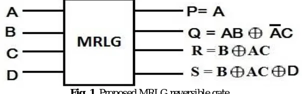
The basic proposed of this Multifunctional Reversible Logic Gate is a reversible logic gate. MRLG have a low power and small delay in design. Fig.1 was the basic approach of this proposed 4X4 reversible MRLG gate. Table 2 shows the MRLG gate truth table. In the truth table of the MRLG input pattern corresponding to a specific output pattern is determined uniquely and to maintain the one-to-one correspondence mapping between the input vector and the output vector. The MRLG input vector is Iv = (A, B, C, D) and there output vector is Ov = (P = A, Q = AB ⊕ A’C,
R = B⊕ AC, S = B⊕ AC ⊕D). It basically consists of two modules, one is made by CMOS and other is by PTL (Pass transistor logic). Both techniques have various disadvantages and advantages.
Fig. 1. Proposed MRLG reversible gate.
Table 2: Proposed MRLG gate truth table
Input Output Input Output A B A B C D P Q A B A B C D P Q
0 0 0 0 0 0 0 0 1 0 0 0 1 0 0 0 0 0 0 1 0 0 1 0 1 0 0 1 1 0 1 0 0 0 1 0 0 1 0 0 1 0 1 0 1 0 1 1 0 0 1 1 0 1 1 0 1 0 1 1 1 0 0 1 0 1 0 0 0 0 1 1 1 1 0 0 1 1 1 1 0 1 0 1 0 0 0 1 1 1 0 1 1 1 0 1 0 1 1 0 0 1 1 1 1 1 1 0 1 1 0 0 0 1 1 1 0 1 0 1 1 1 1 1 1 1 1 0
A. CMOS realization of MRLG gate:
B. Pass transistor realization of MRLG gate:
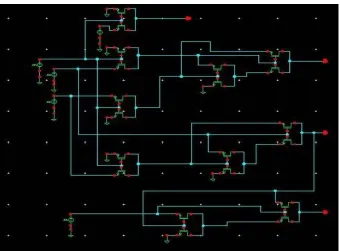
The Pass transistor logic (PT) realization of MRLG gate is shown in fig.3. Consider the input are A= ‘1’, B= ‘1’, C= ‘0’ and D= ‘1’. Since A= ‘1’ the transistor Q1 is OFF and Q2 is ON. So the output P= ‘1’. Since A= ‘1’, B= ‘1’ and C= ‘0’, Q4, Q7,Q10 are ON and Q3, Q5, Q6, Q8, Q9 are OFF So the output Q= ‘1’. And Q12, Q13, Q16 are ON and Q11, Q14, Q15 are OFF, so the output R= ‘1’. Since A= ‘1’, B= ‘1’, C= ‘0’ and D= ‘1’, Q17, Q20 are ON and Q18, Q19 are OFF. So the output S= 0. Transistors count in MRLG gate in CMOS realization technique is 20.
IV. RESULT AND DISCUSSION
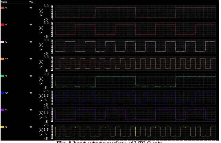
Fig. 4. Input output waveform of MRLG gate
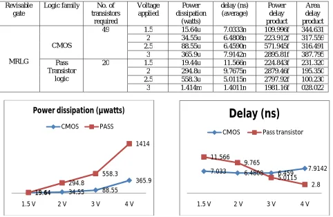
Table 3 and Table 4 give the output parameters and the comparisons between the Pass transistor logic and CMOS realization of MRLG gate. In this paper observed the propagation delay for all input to all output like A → P, A→ Q, A → R, A →S, B → P, B → Q, B→R, B →S, C → P, C → Q ,C → R, C → S, D→P, D → Q, D → R and D →S . In Table 3 tabulated the average of propagation delay of MRLG gate for applied voltage in different design techniques (CMOS and Pass transistor logic) for inputs A, B, C and D to Output P, Q, R, and S.
Table 3. Delay of MRLG gate for applied voltage in different design techniques (CMOS and Pass transistor logic)
CMOS Logic Pass Transistor Logic Voltage
applied
1.5 2 2.5 3 1.5 2 2.5 3
Delay 1 (ns)
A to P 23.74 23.8 23.79 48.89 .2110 .5385 .4447 .3730 A to Q .3866 .5728 .7254 .9025 .4734 .5385 .4910 .5338 A to R .628 .8941 1.025 1.135 49.91 36.42 11.25 1.04 A to S 1.119 1.18 1.22 1.25 .7738 .8953 .9879 .9235
Avg. 6.4684 6.6117 6.6901 13.044 12.842 9.5980 3.2934 .7175 ‘
Delay 2 (ns)
B to P 24.46 24.52 24.5 49.61 .7743 1.189 1.165 1.14 B to Q .3334 .1472 .0054 .2005 .0599 .2211 .2290 .2329 B to R .09129 .1741 .3048 .415 56.46 37.50 11.97 .2735 B to S .3992 .4602 .5002 .529 .2405 .2453 .2679 .1568 Avg. 6.3209 6.3253 6.326 2.6886 14.384 9.7888 3.4079 .4508
Delay 3 (ns)
Delay 4 (ns)
D to Q .8734 .6872 .5346 .3395 .4596 .7112 .7440 .7690 D to R .6313 .3659 .2552 .1249 50.85 36.56 36.56 12.51 D to S . 1408 .0784 .0398 .01046 .1565 .2422 .2721 .2721 Avg. 8.8349 6.5479 6.4674 3.9062 13.153 9.7976 9.8110 3.816
Total delay (ns) 7.0333 6.4808 6.459 7.9142 11.566 9.7675 5.0115 1.4011
In Table 4. Shows the average power dissipation calculated for the entire input bit pattern. In comparison of different techniques, the advantage of this design is not only depends on transistor count, delay, and power but also on AT (transistor count (area) and delay product) and PDP (power and delay product) values. The comparisons of transistors count, Power dissipation, Delay, PDP and AT are shown in Table 4.
Table 4. Synthesis results of MRLG using CMOS and Pass transistor logic
Revisable gate
Logic family No. of transistors
required
Voltage applied
Power dissipation
(watts)
delay (ns) (average)
Power delay product
Area delay product
MRLG
CMOS
49 1.5 15.64u 7.0333n 109.996f 344.631 2 34.55u 6.4808n 223.912f 317.559 2.5 88.55u 6.4590n 571.945f 316.491 3 365.9u 7.9142n 2895.81f 387.795 Pass
Transistor logic
20 1.5 19.44u 11.566n 224.843f 231.320 2 294.8u 9.7675n 2879.46f 195.350 2.5 558.3u 5.0115n 2797.92f 100.230 3 1.414m 1.4011n 1981.16f 028.022
Fig. 5. Power analysis of MRLG gate. Fig. 6. Delay analysis of MRLG gate
V. APPLICATION OF MRLG GATE
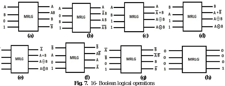
By using MRLG gate we can do design 16 Boolean logical operations. We know that Binary logic (Base = 2) has two logical states 0 and 1. Depending on the number of used variables and base, different logic functions can be generated. The number of possible Boolean function is [17]
N = B
Where n is the number of variables and B is the Base. In binary logic (B=2) of two variables (n=2), the no. of Boolean function is N = B = 2 = 16. Table 5.shows the all possible Boolean functions of two variables.
15.64 34.55 88.55
365.9
19.44
294.8
558.3
1414
1.5 V 2 V 3 V 4 V
Power dissipation (µwatts)
CMOS PASS
7.033 6.4808 6.459 7.9142
11.566
9.765
5.0115 2.8
1.5 V 2 V 3 V 4 V
Delay (ns)
Table 5. Sixteen Boolean Logical Functions (F1-F16).
Input A 0 0 1 1 Input A 0 0 1 1 B 0 1 0 1 B 0 1 0 1
Output
F1 0 0 0 0 False (0)
Output
F9 1 0 0 0 A'B' F2 0 0 0 1 AB F10 1 0 0 1 A B F3 0 0 1 0 AB' F11 1 0 1 0 B' F4 0 0 1 1 A F12 1 0 1 1 A+B' F5 0 1 0 0 A'B F13 1 1 0 0 A' F6 0 1 0 1 B F14 1 1 0 1 A'+B F7 0 1 1 0 AB F15 1 1 1 0 A'+B'
F8 0 1 1 1 A+B F16 1 1 1 1 True (1)
We can apply any one of the light sources A, B, 0 (zero power supply), or 1 (constant power supply) to the all 4 inputs (A, B, C, and D) of the MRLG gate, we get all sixteen Boolean operations as shown in Table 5 according to Fig. 7 (a)– (h).
(a) (b) (c) (d)
(e) (f) (g) (h) Fig. 7. 16- Boolean logical operations
VI. CONCLUSION
In this paper approach to design of new reversible logic 4x4 Multifunctional Reversible Logic Gate. Circuits are implemented in transistor level with different design techniques Pass transistor logics (PT) and CMOS. And compare their performance by different supply voltage 1.5 to 4 V (1.5V, 2V, 3V, 4V). In this paper Conclude that the design of a multifunctional reversible gate for a reversible digital designs that can be minimizing the power consumption, delay, garbage outputs and quantum cost. After that, we observe a different property of the reversible MRLG gate in compare to the other alternative reversible gate. MRLG can design sixteen Boolean logical operations. Fig.7. Shows the sixteen Boolean operations and clear that in this case there in no garbage.
VII. FUTURE SCOPE
REFERENCES
1. Bennett, C.H., “Logical Reversibility of Computation”, IBM Journal Research and Development, 525-532. 1973.
2. Azad Khan, M.H, “Design of Full-Adder with Reversible Gates”, International Conference on Computer and Information Technology, Dhaka,
Bangladesh, pp: 515-519. 2002.
3. Bisdounis, L., D. Gouvetas and O. Koufopavlou, “A comparative study of CMOS circuit design styles for low-power high-speed VLSI
circuits”. International Journal of Electronics, 599-613. 1998.
4. Chatzigeorgiou, A. and S. Nikolaidis, “Modeling the operation of pass transistor and CPL gates”, International Journal Electronics, 977-1000,
2001.
5. Feynman, R., “Quantum Mechanical Computers”, Optic News, 11-20, 1985.
6. Fredkin, E. and T. Toffoli, “Conservative Logic”, International Journal of Theoretical Physics. 219-253. 1982.
7. Himanshu Thapliyal and Nagarajan Ranganathan, “A New Design of the Reversible Subtractor circuit”, 11th IEEE international Conference
Nanotechnology, 2011.
8. Himanshu Thapliyal and M.B. Srinvas, “Novel Reversible TSG gate and Its Application for Designing Components of Primitive Reversible/
Quantum ALU”, ICICS 2005.
9. Krishnaveni, D. and M. Geetha Priya, “Design of Reversible Serial and Parallel Novel Adder/Subtractor”, International Journal of Engineering
Science and Technology; (IJEST) march. 2011.
10. Landauer, R., “Irreversibility and Heat Generation in the Computing Process”, IBM Journal Research and Development, 183-191, 1961.
11. Majid haghparast and Keivan Navi, “A Novel Reversible Full Adder Circuit for Nanotechnology Based Systems”, Journal of Applied Sciences,
3995-4000, 2007.
12. Maslov, D., D.M. Miller and. G.W. Dueck, “Techniques for the Synthesis of Reversible Toffoli Networks”, ACM Transaction Design
Automated Electronic System, 2007.
13. Morgenshtein, A, A. Fish and I.A. Wagner, “Gate-diffusion input (GDI): A power-efficient method for digital combinatorial circuits”, IEEE
Transaction on VLSI, 566-581, 2002.
14. Peres, A., “Reversible Logic and Quantum Computers”, Physical Review, 3266-3276. 1985.
15. Rashmi, S.B. and B.G. Tilak, “Transistor Implementation of Reversible PRT gates”, International Journal of Engineering Science and
Technology,2011.
16. Toffoli, T., “Reversible Computing”, Tech Memo MIT/LCS/TM-151, MIT Lab for Computer Science, 1980.
17. R. Cunha, H. Boudinov, and L. Carro, “Quaternary look-up tables using voltage-mode CMOS logic design,” in Proc. 37th Int. Symp. Multiple
Valued Logic (ISMVL’07), p. 56.
BIOGRAPHY
Vinay Kumar pursuing M.E in the branch of Electronics VLSI Design at PEC University of Technology Chandigarh, India.