ABSTRACT
DE, ANKAN. Device Characterization, Hardware Implementation and System Analysis of Soft switched AC/AC Converters. (Under the direction of Dr. Subhashish Bhattacharya). Conventional AC-to-DC rectification topology using nonlinear devices, for example diode or thyristor bridges, causes input current harmonics and unwanted reactive power. This effectively deteriorates the voltage and current waveform of the utility grid. Owing to hard switched operation these converters have high switching loss, low frequency of operation, high device stress and are bulky in size. A lot of research has been carried out in the last two decades towards high frequency link dc-dc and dc-ac converters. Various AC-AC converters have also been proposed in the form of cycloconverters and matrix converters. These converters are attributed with complicated controller design, limited buck and boost operation, considerable amount of switching losses and non-favorable frequency changing operation.
The understudied research investigates soft-switching high frequency link AC/AC converters. A number of proposed converters are presented which overcomes the various shortcomings of conventional AC Link schemes. The switching operations occur at zero voltage instants thus lowering the switching losses. The input and output current is harmonic free and the controller also allows setting of desired power factor with buck and boost operations and bi-directional power flow capability.
been noticed and presented. The main motivation of this part of the work is to make a fair judgment on device selection for various soft-switch based topologies.
An in-depth analysis has been done to study optimized module design for series connection of switch and diode. The modules are 3D printed to offer low cost testing of modules. They have been tested up to 4kV in voltage and 100A in current. A DC-DC converter has been built using these modules. The system was stable at full VA rating of the devices.
A modified Steinmetz equation based optimization study has been conducted to analyses magnetics design for DynaC and Partial Resonant converters. The effectiveness of these designs have been shown with corresponding hardware test. The designs showed improvement in efficiency and thermal stability.
Device Characterization, Hardware Implementation and System Analysis of Soft switched AC/AC Converters
by Ankan De
A dissertation submitted to the Graduate Faculty of North Carolina State University
in partial fulfillment of the requirements for the degree of
Doctor of Philosophy
Electrical Engineering
Raleigh, North Carolina 2015
APPROVED BY:
_______________________________ _______________________________ Dr. Subhashish Bhattacharya Dr. Mesut Baran
Committee Chair
_______________________________ _______________________________
ii
DEDICATION
iii
BIOGRAPHY
Ankan De received his Bachelor of Technology degree in Energy Engineering under the Department of Electrical Engineering from Indian Institute of Technology, Kharagpur in 2009. After graduation, he worked in IBM-ISL as an Associate Software Engineer from Jan, 2010 till June, 2010.
He joined the FREEDM Systems Center as an Integrated PhD student at NC State University in Fall, 2010. He received Student Exchange Fellowship to conduct research in ETH-Zurich in 2013. He was awarded the IEEE SUOZZI Intelec Fellowship for the year of 2013 in Hamburg, Germany. He also received Travel fellowship to attend T&D 2014 Conference in Chicago and InterPACK 2015 in San Francisco. He started working in Texas Instruments in Bethlehem, PA from Feb, 16 onwards.
His research interests include Power Electronics, High Frequency Magnetics and High Voltage Packaging. He specializes in AC/AC, resonant and soft switched Converters.
iv
ACKNOWLEDGMENTS
I would like to convey my deepest gratitude and regard towards my advisor, Dr. Subhashish Bhattacharya. Under his guidance, I metamorphosed from an unruly undergrad to an Industry grade Professional. The work presented in this thesis is a result of years of constant inspiration and mentorship under him.
I would like to thank the rest of my thesis committee members: Dr. Mesut Baran, Dr. Jayant Baliga and Prof. Xiangwu Zhang for their patience and guidance.
My sincere thanks goes to all the staff and students at NSF FREEDM Systems Center at North Carolina State University who kept the center running and thus, facilitated my research work. I am especially thankful to my colleague, Dr. S. Roy, who greatly assisted me in building and implementing some of the more complicated portions of my research. I would also like to thank Adam Morgan for his support both in and outside the work place.
v
TABLE OF CONTENTS
1. INTRODUCTION... 1
1.1 Context ... 1
1.2 Overview Of Various AC/AC Converters ... 2
1.2.1 Back-to-Back Voltage Source Converters ... 2
1.2.2 Matrix Converter ... 2
1.2.3 Integral Solid State Transformer (SST) Structure ... 3
1.2.4 Resonant AC-Link Converter ... 4
1.2.5 Isolated Dynamic Current Converters (DynaC) ... 5
1.2.6 Partial Resonant Link Converter ... 6
1.2.7 Converter Based Research Focus ... 7
1.3 Current Switch Device Characterization... 7
1.4 Optimum Module Design ... 9
1.5 Optimized Magnetics Design ... 10
1.6 Dynamic VAR Compensator ... 11
1.7 Chapter Outline ... 12
2. DYNAMIC CURRENT (DYNAC) BASED CONVERTER SYSTEM... 15
2.1 Introduction ... 15
2.2 Principle Of Operation ... 17
2.3 Improvement in Reverse Recovery Current ... 23
2.4 Soft Switched Turn-Off Enabled By SiC-JBS Diode ... 25
2.5 System Dynamic Equations ... 27
2.6 Governing Equations and Controller Block Diagram ... 31
2.7 Simulation Results ... 32
2.8 Experimental Results ... 35
2.9 Converter System with Integrated Battery Storage ... 37
vi
2.10.1 Converter Topology ... 41
2.10.2 Principle of Operation ... 42
2.10.3 Experimental Results ... 45
2.11 Sparse AC/DC Converter ... 47
2.11.1 Principle Of Operation ... 50
2.11.2 Device Based Efficiency Comparison ... 54
2.11.3 Prior Art Comparison ... 56
2.12 Conclusions ... 57
3. PARTIAL RESONANT LINK CONVERTER SYSTEM ... 59
3.1 Introduction ... 59
3.2 Proposed Bidirectional Soft-Switched Sparse AC/AC ... 60
3.3 Hardware Test ... 69
3.4 Device Performance and Selection ... 71
3.5 Three-Phase Four-Switch Soft Switched Rectifier with High Frequency Isolation 73 3.5.1 Proposed topology ... 73
3.5.2 Hardware Test ... 79
3.5.3 Prior Art Comparison ... 79
3.6 Conclusions ... 80
4. PERFORMANCE COMPARISON, CHARACTERIZATION AND DESIGN OPTIMIZATION OF CURRENT SWITCH ... 81
4.1 Introduction ... 81
4.2 Reverse Voltage Commutation ... 82
4.3 Switch Overlap Loss Analysis ... 85
4.4 Hard Switch Test... 87
4.5 Forward Characteristics ... 89
4.6 Converter Test ... 90
vii
4.7.1 Test Circuit And Principle of Operation ... 93
4.7.2 Hardware Test Results ... 97
4.7.3 Basic Principle Of Operation Of Resonant AC-Link Converter ... 102
4.7.4 Switch Loss Estimation Of Resonant AC-Link Converter ... 104
4.8 Conclusion ... 107
5. DESIGN CONSIDERATIONS OF PACKAGING A HIGH VOLTAGE CURRENT SWITCH ... 108
5.1 Introduction ... 108
5.2 Principle Stress And Operations Of Current Switch ... 110
5.3 Primary Topologies of current switch ... 115
5.4 Parasitic Extraction ... 118
5.5 Current And Electric Field Distribution ... 119
5.6 Thermal Study ... 120
5.7 Maximum Attainable Frequency... 122
5.8 Stacked Bond Wire Topology ... 125
5.9 Hardware Testing Results ... 127
5.10 Conclusion ... 128
6. MAGNETICS DESIGN... 130
6.1 Introduction ... 130
6.2 Loss Prediction and Inductor Proposal ... 131
6.3 Derivation of Steinmetz Parameters ... 131
6.4 Preferred Core Geometries ... 133
6.5 Variation of Weight and Losses as a function of Inductor Parameters ... 134
6.6 Proposed Inductor Structures ... 136
6.7 Uniform Flux Magnetics Design using non-uniform Magnetic Material ... 137
6.7.1 Introduction ... 137
6.7.2 Applications ... 138
viii
6.8 Conclusion ... 144
7. DVC MODELLING AND VOLT-VAR CONTROL FOR DISTRIBUTION FEEDERS** ... 145
7.1 Introduction ... 145
7.2 The Feeder Model ... 147
7.3 Proposed Power Electronic DVC ... 147
7.3.1 Principle Of Operation ... 148
7.3.2 Simulation Results And Initial Hardware Results ... 150
7.4 Dynamic Model of DVC ... 151
7.5 Study cases ... 152
7.5.1 Time-invariant Load with VRs ... 152
7.5.2 Time-variant Load with DVC at node 890 and VRs ... 156
7.5.3 No VRs ... 159
7.6 PV Impact on a Distribution System ... 167
7.7 Conclusions ... 174
8. DETERMINATION OF ELECTRIC FIELD STRESS DISTRIBUTION IN SOLID STATE TRANSFORMERS AND EVALUATION OF TEST METHODS .... 175
8.1 Introduction to Solid State Transformers ... 175
8.2 Modular Cascaded SST ... 176
8.3 Critical Voltage Stress ... 178
8.4 Phase-shifted Multi-level Converter ... 179
8.4.1 Simulation Results ... 179
8.4.2 Inter Module Voltage Stress ... 181
8.4.3 Voltage Stress on Transformer winding with respect to ground ... 182
8.4.4 Voltage difference across middle point of Transformer ... 183
8.4.5 Voltage difference across the top point of Transformer ... 184
8.4.6 Voltage difference across diagonal points of Transformer ... 185
ix
8.5 Optimized module control algorithm ... 187
8.6 Voltage Stress on Transformer as a function of Control Algorithm ... 188
8.6.1 Linear Delay ... 189
8.6.2 Zig-zag Delay ... 190
8.6.3 Reverse Zig-zag Delay ... 192
8.6.4 Optimized module control algorithm ... 192
8.6.5 FFT Comparison ... 194
8.7 Chaotically jittered phase-shifted Multi-level Converter Algorithm ... 195
8.8 COMSOL Simulation Results ... 197
8.9 Prediction of ageing and material selection ... 200
8.10 Introduction to Dielectric Heating ... 201
8.11 Harmonic Power Factor and Total Dielectric Loss ... 204
8.12 Proposal for Experimental Test Setup ... 205
8.13 Choice of Electrode Configuration ... 206
8.14 COMSOL Simulation of Electrode System with Tapped Wedges ... 209
8.15 Conclusion ... 211
9. CONCLUSIONS ... 213
x
LIST OF FIGURES
Figure 1.1: Back-to-Back Voltage Source Converters for AC/AC Power Conversion ... 2
Figure 1.2: Circuit Schematic of a Matrix Converter ... 2
Figure 1.3: Solid State Transformer Structure ... 3
Figure 1.4: Resonant AC-Link Converter ... 4
Figure 1.5: Circuit schematic of Isolated Dynamic Current Converters ... 5
Figure 1.6: Partial Resonant Link Converter Structure ... 6
Figure 2.1: Circuit Schematic of a Conventional SST ... 15
Figure 2.2: Circuit Schematic of Dyna-C. ... 16
Figure 2.3: Three Phase sinusoidal Input V-I waveform divided into six sectors ... 18
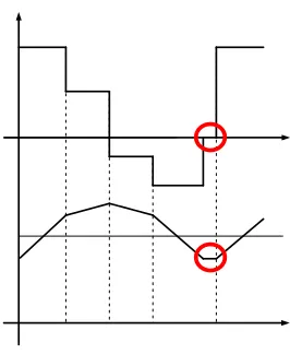
Figure 2.4: Link Voltage and Current ... 19
Figure 2.5: Active Switches in Mode 1 ... 19
Figure 2.6: Active Switches in Mode 2 ... 20
Figure 2.7: Link Voltage and Current ... 20
Figure 2.8: Link Voltage and Current ... 21
Figure 2.9: Active Switches in Mode 3 ... 21
Figure 2.10: Link Voltage and Current ... 21
Figure 2.11: Active Switches in Mode 4 ... 21
Figure 2.12: In Zero-Vector Mode, all switches are turned off ... 22
Figure 2.13: The Link voltage and current in Zero-Vector Mode ... 22
Figure 2.14: The Link voltage and current during zero vector mode ... 24
Figure 2.15 : The Link voltage and current of Conventional DynaC ... 24
Figure 2.16: The Link voltage and current for alternative control scheme ... 26
Figure 2.17: Block diagram of the closed loop system ... 32
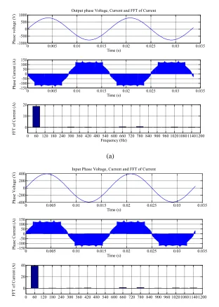
Figure 2.18(a) Input Phase Profile (b) Output Phase Profile ... 33
Figure 2.19(a) Input Phase Profile(b) Output Phase Profile ... 34
Figure 2.20(a) Input Phase Profile(b) Output Phase Profile ... 35
Figure 2.21: Primary winding voltage of the fly-back transforme ... 36
Figure 2.22: Hardware Testing Setup ... 36
Figure 2.23: Input phase voltage and current for Harmonic Free controller ... 36
Figure 2.24: Input phase voltage and current for simplified controller ... 36
Figure 2.25: Converter structure with the integrated battery energy storage system ... 37
Figure 2.26: DC inductor (L1) voltage and current at steady state ... 38
Figure 2.27: Voltage and current of the winding W1. ... 39
Figure 2.28: Voltage and current of the winding W1 ... 39
Figure 2.29: Voltage and current of the winding W3 ... 40
xi
Figure 2.31: Conventional railway traction motor drive system ... 41
Figure 2.32: Proposed cascaded converter topology for the railway traction drive system ... 43
Figure 2.33: A section of the cascaded converter ... 43
Figure 2.34: Fly-back inductor Charging (left) and Discharging (right) ... 44
Figure 2.35: Primary winding voltages of the top (ch1) and middle (ch2)... 46
Figure 2.36: Primary winding voltages of the top (ch1) and bottom (ch2) ... 46
Figure 2.37: Top fly-back transformer primary voltage (ch 1) and the DC output voltage ... 47
Figure 2.38: Circuit Schematic of a Conventional AC/DC with Isolation ... 47
Figure 2.39: Circuit Schematic of AC/DC version of DynaC ... 48
Figure 2.40: Three-Phase Three-Switch Buck Rectifier ... 49
Figure 2.41: Circuit schematic of the proposed Sparse Dyna-C Rectifier ... 49
Figure 2.42: Three Phase sinusoidal Input V-I waveform divided into six sectors ... 50
Figure 2.43: In Mode 1, S1 and S2 are the Active conducting switches. ... 51
Figure 2.44: The Link voltage and current in Mode 1 (red) ... 51
Figure 2.45: In Mode 2, S1 and S3 are the Active conducting switches. ... 52
Figure 2.46: The Link voltage and current in Mode 2 (red) ... 52
Figure 2.47: In Mode 3, S4 is the only Active conducting switches. ... 53
Figure 2.48: The Link voltage and current in Mode 3 (red) ... 53
Figure 2.49: In Zero-Vector Mode all the switches are turned off ... 54
Figure 2.50: The Link voltage and current in Zero-Vector Mode ... 54
Figure 2.51: Device Test under typical switch overlap condition for Si-IGBT. ... 55
Figure 2.52: Device Test under switch overlap condition for SiC-MOSFET ... 55
Figure 2.53: Current Switch undergoing ZCS: Diode Voltage (Blue) and Current (Green) .. 56
Figure 3.1: Circuit Schematic of the proposed topology ... 61
Figure 3.2 (a): Controller Diagram Figure 3.2 (b): Link reference ……….………. 61
Figure 3.3 (a): In Subsystem 1, S1 and S4 are the Active conducting switches. ‘’ ... 62
Figure 3.4 (a): In Subsystem 2, the Link ‘LC’ partially resonated ... 63
Figure 3.5 (a): In Subsystem 3, S1 and S6 are the Active conducting switches. ... 64
Figure 3.6 (a): In Subsystem 4, the Link ‘LC’ partially resonated ... 65
Figure 3.7 (a): In Subsystem 5, T2 and T3 are the Active conducting switches. ... 66
Figure 3.8 (a): In Subsystem 6, the Link ‘LC’ partially resonated ... 67
Figure 3.9 (a): In Subsystem 7, T2 and T5 are the Active conducting switches. ... 67
Figure 3.19: Circuit Schematic of the proposed topology ... 74
Figure 3.20: Controller - Input Current Reference Predictor ... 74
Figure 3.21: In Mode 1, S1 and S2 are the Active conducting switches. ... 75
Figure 3.22: Link Voltage and Inductor Current in Mode 1 ... 75
Figure 3.23: In Mode 2, the Link ‘LC’ resonates partially ... 76
xii
Figure 3.25: Link Voltage and Inductor Current in Mode 3 ... 77
Figure 3.26: In Mode 3, S1 and S3 are the Active conducting switches. ... 77
Figure 3.27: In Mode 4, the Link ‘LC’ resonates partially ... 77
Figure 3.28: Link Voltage and Inductor Current in Mode 4 ... 78
Figure 3.29: Link Voltage and Inductor Current in Mode 5 ... 78
Figure 3.30: In Mode 5, T is the Active conducting switches. ... 78
Figure 3.31: Snapshot of Link Voltage (blue) and Inductor Current (purple) ... 79
Figure 4.1: Device Test Circuit Schematic ... 82
Figure 4.2: Possible Current Switch Configurations ... 83
Figure 4.3: Switching sequence of S1 and S2... 84
Figure 4.4: Switching Characteristics of Si-IGBT and Si-Diode under RVC ... 84
Figure 4.5: Switching Characteristics of RB-IGBT ... 85
Figure 4.6: Comparison of loss between Si-Diode, SiC-JBS Diode, RB-IGBT... 84
Figure 4.7: Device characteristics of the leg with lower voltage for RB-IGBT ... 86
Figure 4.8: Device characteristics of the leg with lower voltage for Si-IGBT ... 86
Figure 4.9: Device characteristics of the leg with lower voltage for SiC-MOS ... 86
Figure 4.10: Forward Characteristics Comparison ... 90
Figure 4.11: Typical LUT in PLECS ... 91
Figure 4.12: Test Circuit for ZCS Characterization... 93
Figure 4.13: Capacitor Voltage and Current for Vin=1000V ... 94
Figure 4.14: Switch Voltage and Current under ZCS turn on and off ... 94
Figure 4.15: Test Circuit for Hard Switched Characterization ... 96
Figure 4.16: Capacitor Voltage and Current for V1 = 500V and V2 = 2500V ... 96
Figure 4.17: Switch (T2) Voltage and Current under hard switched turn-on condition ... 97
Figure 4.18: Switch (T1) Voltage and Current under hard switched turn-off condition ... 97
Figure 4.19: Switch Voltage and Current under zero current switch ... 98
Figure 4.20: Switch Voltage and Current under zero current switch ... 98
Figure 4.21: Switch Voltage and Current under zero current switch ... 99
Figure 4.22: Zoomed-in view of the Switch Voltage and Current under zero current switched turn on and off condition for Vin=1000V ... 99
Figure 4.23: Switch (T1) Voltage and Current under non-zero current switched turn off condition for V1=250V and V2=1000V ... 100
Figure 4.24: Switch (T1) Voltage and Current under non-zero current switched turn off condition for V1=1000V and V2=1500V ... 100
Figure 4.25: Zoomed-in Waveform of Switch (T1) Voltage and Current under non-zero current switched turn off condition for V1=1kV and V2=1.5kV ... 100
Figure 4.26: Switch (T2) Voltage and Current under non-zero current switch ... 101
xiii
Figure 4.28: Zoomed-in Waveform of Switch (T2) Voltage and Current ... 102
Figure 4.29: Circuit Schematic of the understudied Resonant AC-Link Converter ... 103
Figure 4.30: Typical voltage and current transitions of the link capacitor during one ... 104
Figure 4.31: Variation of Turn-On Loss of SiC-Thyristor + SiCJBS Diode switch ... 105
Figure 4.32: Variation of Turn-Off Loss of SiC-Thyristor + SiCJBS Diode switch t ... 105
Figure 4.33: Forward Characteristics of 10kV/10A SiC-JBS Diode ... 105
Figure 4.34: Forward Characteristics of 6.5kV/40A SiC Thyristor... 106
Figure 4.35: Converter Efficiency as a function of throughput power ... 106
Figure 5.1: General Structure and components of a typical package ... 109
Figure 5.2: Test Circuit Schematic with minimal parasitic inductance ... 110
Figure 5.3: Inductor Voltage and Current for the Test setup shown in Figure 2 ... 111
Figure 5.4: IGBT Voltage and Current Transient for the Test setup ... 111
Figure 5.5: Test Circuit incorporating series parasitic inductance ... 113
Figure 5.6: IGBT Voltage corresponding to test-setup ... 114
Figure 5.7: Test Circuit incorporating parallel parasitic capacitance ... 114
Figure 5.8: IGBT Current corresponding to test-setup ... 115
Figure 5.9 (a): Schematic of Cathode-Collector Connected Current Switch ... 116
Figure 5.10(a): Schematic of Emitter-Anode Connected Current Switch ... 117
Figure 5.11: Variation of CC,BP , CE,BP and CCAT,BP ... 119
Figure 5.12: Current Distribution in the package ... 120
Figure 5.13: Voltage Distribution in the package ... 120
Figure 5.14: Temperature Distribution in the package with Alumina Substrate ... 123
Figure 5.15: Temperature Distribution in the package with AlN Substrate ... 124
Figure 5.16: Temperature Distribution in the package with BeO Substrate ... 124
Figure 5.17: Peak Package Temperature as a funtion of Overall Loss of IGBT+Diode ... 125
Figure 5.18: ANSYS Q3D single stacked bond wire (N=1) ... 126
Figure 5.19: Stacked 15mil Al wire bonds from IGBT to diode ... 126
Figure 5.20: Custom, fabricated CSCSP – DBC based ... 127
Figure 5.21: High-V double pulse test setup of CSCSP (A: CSCSP module, B: 10kV/10A SiC JBS diode, C: 8mH inductor, D: 250µF capacitor bank, E: gate driver, F: high-V probe, G: high-BW current probe) ... 127
Figure 5.22: Turn-on transition of CSCSP at 2300V ... 128
Figure 5.23: Turn-off transition of CSCSP at 4000V ... 128
Figure 6.1: Typical Core Loss as a function of Flux Density ... 131
Figure 6.2 (a): A 30 turns Inductor structure (b) 25 turns Inductor structure ... 133
Figure 6.3: A generic inductor structure. ... 133
xiv Figure 6.5: Overall Power Loss in Watts as a function of number of turns and air gap length
... 135
Figure 6.6: Uneven Distribution of Magnetic Field in uniform Toroidal Core ... 139
Figure 6.7: Magnetic Field Distribution in the toroidal cores of the Co-axial Transformer mentioned in Figure 3 ... 140
Figure 6.8: 3D model of the Co-axial Transformer ... 139
Figure 6.9: Distribution of Magnetic Field in non-uniform Toroidal Core. It uses ten different concentric cores of proportionally adjusted relative permeability ... 141
Figure 6.10: Distribution of Magnetic Field in non-uniform Toroidal Core. It uses two different concentric cores of proportionally adjusted relative permeability ... 141
Figure 6.11: Magnetic Field Distribution in the toroidal cores of the Co-axial Transformer. The core can been divided into three concentric hollow cylinders of linearly increased relative permeability ... 142
Figure 6.12: Air gap losses due to fringing flux in an inductor ... 142
Figure 6.13:(a) [Left] Core with lower permeability at the outer layers and higher towards the middle, (b) [Middle] Core with uniform permeability and (c) [Right] Core with higher permeability at the outer layers and lower in the middle. ... 143
Figure 7.1: IEEE-34 Bus Feeder ... 146
Figure 7.2: Circuit schematic of DVC ... 147
Figure 7.3: Three Phase sinusoidal Input Voltage divided into six sectors (green: A, red: B and blue: C) ... 149
Figure 7.4: Three Phase sinusoidal Input Reference Current divided into six sectors (green: A, red: B and blue: C) ... 149
Figure 7.5: Triangular shaped current of Phase C in sector 1 ... 150
Figure 7.6: Phase Voltage and unfiltered phase current ... 151
Figure 7.7: Hardware test result; (blue): voltage; (pink): current ... 151
Figure 7.8: (a) DVC Dynamic Model; (b) DVC Control (simplified) ... 152
Figure 7.9: Voltage Profile for the Base Feeder at Peak Load Condition ... 152
Figure 7.10: (a) Voltage Regulator 2 Tap change Profile;(b) Voltage Regulator 1 Tap change Profile ... 153
Figure 7.11: (a) Voltage Regulator 2 Tap change Profile; (b) Voltage Regulator 1 Tap change Profile………. ... 153
Figure 7.12: Voltage Profile for the Base Feeder with Shunt Capacitor at 848 in Peak Load Condition... 154
Figure 7.13: Voltage Profile for the Base Feeder DVC at 848 in Peak Load Condition ... 154
Figure 7.14: (a) Voltage Regulator 2 Tap change Profile; (b) Voltage Regulator 1 Tap change Profile……….. ... 155
xv Figure 7.16: TAP Change Profile Comparison in Peak Load Condition of Voltage Regulator
1 (left) and 2 (right)... 156
Figure 7.17: Voltage Profile Comparison at 12:30 PM (Low Load) ... 157
Figure 7.18: Voltage Profile Comparison at 10:30 AM (High Load) ... 157
Figure 7.19: Voltage Profile Comparison at 7:30 PM (Peak Load) ... 158
Figure 7.20: Voltage waveform at 890 throughout the day with step change input DVC ... 159
Figure 7.21: Voltage waveform at 890 with closed loop DVC ... 159
Figure 7.22: Voltage Profile for the Base Feeder at Peak Load Condition without VRs ... 160
Figure 7.23: Voltage Profile for 3 DVC under Peak Load Condition ... 161
Figure 7.24: Voltage Profile Comparison for 3 DVC under Peak Load Condition ... 161
Figure 7.25: Voltage Waveform comparison at node 850 ... 162
Figure 7.26: Voltage Profile under Peak Load ... 163
Figure 7.27: Voltage Profile at 12:30 PM (Light Load) ... 164
Figure 7.28: Voltage Profile at 10:30 (High Load) ... 165
Figure 7.29 : Voltage Waveform at 832 ... 165
Figure 7.30: Voltage Waveform at 850 ... 166
Figure 7.31: Voltage Waveform at 890 ... 166
Figure 7.32: Normalized PV and Load profiles ... 168
Figure 7.33: Voltage profile at node 890: with or without PV – Case 1 ... 168
Figure 7.34: Feeder voltage profile at 12:30 pm: with or without PV – Case 1 ... 169
Figure 7.35: PV power changes with sun irradiation – Case 2 ... 169
Figure 7.36: Voltage at node 890 following a cloud cover- Case 2 ... 170
Figure 7.37: Speed of Motors in the system – Case 2 ... 170
Figure 7.38: Voltage Profile at node 890 with one DVC – Case 3 ... 171
Figure 7.39: Feeder Voltage Profile under Peak Load Condition – Case 3 ... 171
Figure 7.40: Voltage Profile Comparisons at 12:30 PM (Peak PV) - Case 4 ... 172
Figure 7.41: Voltage Profile at node 890 with three DVCs – Case 4 ... 172
Figure 7.42: Voltage Profiles under cloud condition – Case 4 ... 173
Figure 7.43: Speed of Motors in the system – Case 4 ... 173
Figure 8.1: Circuit Schematic of the understudied SST ... 177
Figure 8.2: Input Voltage, Input Current and Staggered Rectified Output of the system .... 180
Figure 8.3: Inter Module Voltage Stress Study ... 181
Figure 8.4: Inter Module Voltage Stress ... 181
Figure 8.5: Terminals chosen to study Voltage Stress on Transformer winding with respect to ground ... 182
Figure 8.6: Voltage Stress on Transformer winding with respect to ground ... 182
xvi
Figure 8.8: Voltage difference across middle point of Transformer ... 183
Figure 8.9: Chosen Terminals to study the voltage difference across the top point of Transformer... 184
Figure 8.10: Voltage difference across the top point of Transformer... 184
Figure 8.11: Choice of terminals to depict the voltage difference across diagonal points of Transformer... 185
Figure 8.12: Voltage difference across diagonal points of Transformer ... 185
Figure 8.13: Voltage difference across diagonal points of Transformer (negative orientation) ... 186
Figure 8.14: Voltage difference across diagonal points of Transformer ... 186
Figure 8.15: Circuit Schematic of the understudied SST ... 187
Figure 8.16: Input Voltage, Input Current and Rectifier (Input) Voltage ... 187
Figure 8.17: Frequency spectrum depicting Line Frequency Components ... 189
Figure 8.18: Frequency spectrum depicting Rectifier Switching Frequency Components .. 189
Figure 8.19: Frequency spectrum depicting Effective Rectifier Switching Frequency Components ... 190
Figure 8.20: Frequency spectrum depicting Line Frequency Components ... 190
Figure 8.21: Frequency spectrum depicting Rectifier Switching Frequency Components .. 191
Figure 8.22: Frequency spectrum depicting Effective Rectifier Switching Frequency Components ... 191
Figure 8.23: Frequency spectrum depicting Line Frequency Components ... 191
Figure 8.24: Frequency spectrum depicting Rectifier Switching Frequency Components .. 192
Figure 8.25: Frequency spectrum depicting Effective Rectifier Switching Frequency Components ... 192
Figure 8.26: Frequency spectrum depicting Line Frequency Components ... 193
Figure 8.27: Frequency spectrum depicting Rectifier Switching Frequency Components .. 193
Figure 8.28: Bifurcation diagram of Logistic map ... 195
Figure 8.29: Simulink Block Diagram of chaotic number generator ... 196
Figure 8.30: Spectral Peaks of Input Current of a generic Phase shifted Multilevel Converter ... 196
Figure 8.31: Spectral Peaks of Input Current of chaotically jittered Phase shifted Multilevel Converter... 197
Figure 8.32: COMSOL Space Voltage Distribution ... 198
Figure 8.33: COMSOL Geometry ... 198
Figure 8.34: Voltage Profile distribution along the vertical line passing through the center of geometry ... 199
Figure 8.35: COMSOL Space Voltage Distribution ... 200
xvii Figure 8.37: Voltage Profile distribution along the vertical line passing through the center of
geometry ... 200
Figure 8.38: Temperature response curve of the heating of a sample considering only internal heating and convection ... 204
Figure 8.39: Proposed Test Circuit for mixed voltage stress analysis ... 206
Figure 8.40: Voltage Stress on the Dielectric, Magnetizing and Input Current of High Frequency Transformer ... 206
Figure 8.41: Basic Configuration ... 207
Figure 8.42: Basic Configuration with taped wedges ... 207
Figure 8.43: (a) Multiple Grounded Electrodes; (b) Multiple symmetric electrodes ... 208
Figure 8.44: High precision Electrode Configuration ... 208
Figure 8.45: Painted shield with soldered Electrode ... 209
Figure 8.46: Electric Potential Distribution of the system ... 210
Figure 8.47: Electric Potential Distribution of the tapped wedges ... 209
Figure 8.48: Electric Field hotspots of the system without tapped wedges ... 210
1
CHAPTER 1
1. INTRODUCTION
1.1 Context
Electrical power conversion is undoubtedly the major driving force in all industrial sectors. Electrical power control, process automation and system protection are ubiquitous in most modern industrial, domestic, military or aerospace application today. Switched Mode Power Converters have become standard at these applications on account of their operational efficiency. They combine power control, process automation as well as system protection in a convenient way.
The utility provides ac voltage at constant amplitude and frequency. However, many industrial applications require voltage at variable amplitude and frequency at various power levels. This has to be achieved through power electronic converters which accept power from the utility in a fixed from and deliver power in other forms as required by the loads. While the pulse width modulated voltage source converter (PWM-VSC) configuration has been industry's work horse for over 30 years, significant advances in power semiconductor device technology has resulted in a number of cheaper, compact and more efficient power converters [1] - [3]. In general, the following characteristics can be considered desirable in power converters used as interface converters in the high frequency link systems:
• Bidirectional Power flow • Unity input power factor
2
1.2 Overview Of Various AC/AC Converters
1.2.1 Back-to-Back Voltage Source Converters
Figure 1.1: Back-to-Back Voltage Source Converters for AC/AC Power Conversion
Figure 1.1 shows the circuit schematic of a typical back-to-back Voltage Source Converter [4]. The front-end Voltage Source Rextifier performs ac-dc power conversion as well as draws sinusoidal current waveforms from the utility. Cascaded Voltage Source Inverter converts DC voltage to AC of required voltage and frequency.
Advantages: Bidirectional, Simple Controller, Low Conduction Losses, Less number of passive components, Compact.
Disadvantages: Usage of Electrolytic capacitor, High Switching loss/stress, High dv/dt, Usage of snubbers, Lacks Galvanic Isolation, Low Frequency Operation, Bulky passive components.
1.2.2 Matrix Converter
OR OR
M
Figure 1.2: Circuit Schematic of a Matrix Converter
3 Figure 1.2 shows the basic circuit schematic of Matrix Converter [5]. The matrix converter is a direct ac-ac power converter, which connects supply ac utility to output ac load through only controlled bi-directional switches. The output ac signals with adjustable magnitude and frequency are constructed by single- stage power conversion process. The direct ac-ac power conversion principle of the matrix converter leads to the distinct structure with no large dc-link energy storage components. Consequently, the matrix converter topology can be implemented with compact size and volume compared with the diode rectifier based PWM-VSI, where the dc-link capacitor generally occupies 30 to 50 % of the entire converter size and volume.
Advantages: Compact, low Weight/Size, Bidirectional, High Temperature Operation Capability - due to lack of electrolytic capacitor.
Disadvantages: Complicated Control Algorithm, inferior input/output transfer ratio (~86%), limited frequency changing capability, High Switching loss/stress, High dv/dt, Usage of snubbers, Lacks Galvanic Isolation, Low Frequency Operation, Bulky passive components.
1.2.3 Integral Solid State Transformer (SST) Structure
Figure 1.3 shows the basic structure of a typical SST [6]. As compared to Case 1.2.1, here an addition DC/DC Converter is added primarily for isolation. Preferably, as soft switched DC/DC converter are used.
A B C A’ B’ C’
Rectifier DC/DC with Isolation Inverter
4 This way the frequency of operation can be increased and the magnetics size can be considerably reduced.
Advantages: Bidirectional, Simple Controller, High Frequency Operation, Involves Galvanic Isolation.
Disadvantages: Usage of Electrolytic capacitor, High Switching loss/stress (Rectifier/inverter side), High dv/dt, Usage of snubbers, Low Frequency Operation (Rectifier/inverter side), Bulky filters.
1.2.4 Resonant AC-Link Converter
Fig. 1.4 shows the basic structure of this topology [7]. This is a resonant converter which incorporates soft-switching feature and is characterized by negligible switch turn on and low turn off losses [7]-[10]. It follows a two cycle operation. First, a desired charge is drawn from each phase of a power supply to charge an energy storage element. Second, the charge of the energy storage element is discharged through the output of the same. Through repetitive cycles of the above mentioned operation, charge can be extracted from the power source and injected to the output. Since the AC-Link switching losses are almost negligible, due to the soft switching characteristic, the AC-Link can operate at relatively higher switching frequency.
5 This not only reduces the physical size and complexity but also significantly reduces the losses. It also permits the use of high frequency transformers.
Advantages: Low Loss, Galvanic Isolation, High Frequency Operation, Harmonic Free Input Current.
Disadvantages: High Device Blocking Voltage Stress (Due to resonance, the capacitor charges to a voltage twice the input line-line voltage), Complicated Control Algorithm, Limited Buck-Boost and Frequency Change Capability.
1.2.5 Isolated Dynamic Current Converters (DynaC)
Fig. 1.5 shows the basic schematic of this topology. In this converter, at first the phases with maximum voltage are connected to the transformer first (but turning on the appropriate switches). The turn on duration is set such that the average current in the phases meet the set reference. Then the phases with second highest voltage are turned on till the phase currents meet the desired reference. After this stage of operation, similar sets of operation are conducted to discharge the transferred power from the transformer to the output grid. Through repetitive cycles of the above mentioned operation, charge can be extracted from the power source and injected to the output.
Figure 1.5: Circuit schematic of Isolated Dynamic Current Converters
V
aV
bV
cV
o aV
o bV
o cS
1S
2S
3S
4T
1T
2T
3T
4S
5S
6T
5T
66 Advantages: Galvanic Isolation, High Frequency Operation, Harmonic Free Input Current, Simple Controller, Wide Buck Boost and Frequency Capability.
Disadvantages: Need of Snubbers, Hard-Switched Operating states, Reverse Recovery Loss, High Conduction Loss.
1.2.6 Partial Resonant Link Converter
Figure 1.6 shows the basic schematic of this topology [11]. This soft-switched converter uses
12 bidirectional switches and overcomes the various shortcomings of conventional AC Link schemes. The switching operations occur at zero voltage instants thus lowering the switching losses. The input and output current is harmonic free and the controller also allows setting of desired power factor. It can perform buck and boost operations and has bi-directional power flow capability. As the converter operates at high switching frequency, it offers both improved performance and considerable reduction of volume, weight and cost.
Vi1
Vi2
Vi3
S1
S2 S3
S4 S5
S6 T2 T4 T6
T1 T3 T5
C L
Vo1
Vo2
Vo3
Input Filter Output Filter
Figure 1.6: Partial Resonant Link Converter Structure
Advantages: Galvanic Isolation, High Frequency Operation, Harmonic Free Input Current, Wide Buck Boost and Frequency Capability, Snubberless, Soft Switched.
7
1.2.7 Converter Based Research Focus
The prime focus of this thesis will be on DynaC and Partial Resonant Link Converter as mentioned in section 1.2.5 and 1.2.6 respectively. Detailed circuit analysis will be presented in subsequent chapters with various modifications to overcome some of the disadvantages of the system. A number of proposed converters will be presented with simulation and hardware results.
1.3 Current Switch Device Characterization
Over the last couple of decades, a lot of work has been done on converters based on Soft Switching techniques [12-14]. The science behind the typical Zero Voltage Switching (ZVS) characteristics has been presented and an in-depth study has been shown [15]. As most available devices are designed for hard switching applications, very little data is available in the literature on device behavior under Current Switch (series connected switch and diode) based soft switching conditions. The application of current-switch inverters such as the High Frequency Link inverter is being actively considered by many manufacturers [16-18]. As current-switch technology matures, designers push the performance envelope for their circuits until the device once again becomes the limiting factor.
8 behavior under reverse voltage commutation, hard switched and zero current turn off condition at various dc voltage levels are presented. A test circuit has been built and tested with various series connected device combinations, viz. (a) IGBT and Diode, (b) Si-IGBT and SiC-JBS Diode, (c) SiC-MOSFET and SiC-JBS Diode, and (d) Custom Made Package. This work done presents the following device characterizations - (a) Comparison of reverse-recovery losses; (b) Comparison of turn-on Voltage spike (a new form of switching characteristics) for Si-IGBT with SiC-JBS Diode and SiC-MOSFET with SiC-JBS Diode, and (c) Hard Switching loss comparison. The main motivation of this part of the work is to find the best combination of devices to minimize losses and device stress under generic current source converter conditions.
A unique series resonant testing circuit has also been proposed to characterize a 6.5kV SiC Thyristor (GA040TH65). The device has been tested in several soft and hard turn on and off transitions. Conceptual simulation and hardware results have been presented. It has been shown that SiC Thyristor exhibit fast turn-on transitions (~200ns). This coupled with the fact that SiC-JBS Diode (connected in series) has fast reverse voltage commutation leads to an efficient and robust switch combination for a high voltage, high power and high frequency converter. The collected data has been used to estimate overall device losses of a high voltage and high power resonant soft-switched converter.
9 readings have been enumerated in a Look-Up Table for a converter simulation. The overall switch-losses have been plotted as a function of power for a particular frequency rating.
1.4 Optimum Module Design
As these switches are not widely available in market as a unified package, researchers are forced to use series connected discrete switches to form a current switch. Figure 1.7 shows a schematic of such an arrangement.
Terminal
Anti-parallel Diode
Bond Wire
IGBT/MOS
Series Diode
Bus Bar Terminal
Figure 1.7: Package Schematic of Series Connected Discrete Module
Figure 1.7: shows few permutations of this switch.
Figure 1.8: IGBT+Diode (left), MOS+Diode (middle) and RB-IGBT (right)
10 the primary cause of malfunctioning of packages. Reducing the number of necessary bond wires is an important design goal to make the system more robust and efficient.
ANSYS Q3D/MAXWELL software have been used to analyze and extract parasitic inductance and capacitances in the package along with electromagnetic fields, electric potentials, and current density distributions throughout the package for variable parameters. SIMPLIS-SIMETRIX is used to simulate typical switch behavior for different parasitic parameters under hard switched conditions. Various simulation results have then been used to redesign and justify the optimized package structure for the final current switch design. The thermal behavior of such a package is also conducted in COMSOL in order to ensure that the thermal ratings of the power devices is not exceeded, and to understand where potentially harmful hotspots could arise and estimate the maximum attainable frequency of operation. Hardware setup has been made to characterize the device in unit and continuous pulse tests. The main motivation of this work is to enumerate detailed design considerations for packing a high voltage current switch package.
1.5 Optimized Magnetics Design
11 A variable permeability core has also been analyzed. A variable permeability based core as opposed to conventional cores is the fact that the entire core volume is fully utilized to the maximum field strength. This leads to higher inductance for the same/similar volume of the structure. This feature can be used to optimize the size and weight of high frequency magnetics. For transformers, this would result in higher magnetizing inductance thereby reducing the frequency of operation without affecting the size of the converter. For gapped magnetics design, it is shown that certain configuration of permeability variation leads to lower fringing flux which can greatly reduce the overall loss.
1.6 Dynamic VAR Compensator
Utilities try to keep the voltages on a distribution feeder within a target range, and the common practice in United States is to follow the ANSI C84.1 [19] which specifies the range for both service voltage and utilization voltage. On a conventional radial distribution feeder, the common devices employed for voltage control are voltage regulators (VRs) and capacitors. With proper placement of, and coordination between, these Volt-VAR compensators, voltages along a feeder can be kept within acceptable limits under typical load conditions.
Recent interest in connecting small scale renewable energy based generation systems to distribution feeders, partly spurred by the adoption of Renewable Portfolio Standards [20], poses challenges to the conventional Volt-VAR control (VVC) schemes [21]. Connection of large amount of residential scale PV in particular is a challenging case, as it can introduce a highly fluctuating power swing on a distribution feeder [22].
12 operation (voltage control logic, excessive tap movements of VRs and Load Tap Changers, LTCs), and coordination between protection devices [23].
Conventional devices (substation LTC, VRs and Capacitor Banks) employed for VVC on a distribution system act on local information and they are slow acting devices. Hence, these devices respond poorly to voltage variations caused by fast power variations from PVs during a cloudy day. Recently, power electronics based VAR compensators have been proposed to address these challenges, as they can respond to voltage variations much faster and thus provide much more effective VAR compensation on a distribution system [24-25]. In this part of the work, voltage variation issues on a distribution feeder with high PV penetration have been presented first in section II. In section III, the effectiveness of deploying a new type of VAR Compensator, Dynamic VAR Compensator (DVC), in mitigating the voltage variation problems caused by high PV penetration is presented. Section IV provides the conclusions.
1.7 Chapter Outline
Chapter 1 introduces the basic theme of the thesis. Various prior art based power electronic converters are mentioned and a brief introduction of the understudy is mentioned. Reverse Blocking Device characterization is mentioned to show the basic need for this study. One of the section deals with the Dynamic VAR Compensator which may be considered as an immediate practical implementation of the understudied converters.
13 version of this topology has also been proposed. Working principle and hardware results of the same has been presented in details. A sparse AC/DC converter has been proposed with hardware results to confirm the various advantages.
Chapter 3 presents a novel bi-directional soft-switched AC/AC converter. The working principle, simulation and hardware results of the full system have been presented. A sparse AC/DC rectifier has been proposed for Data Center based application. Hardware results of the same have been presented. A brief guide has been given for device selection.
Chapter 4 deals with reverse blocking device characterization. Reverse Voltage Commutation, Switch Overlap Characteristics, Hard Switched, and Forward characteristics of various suitable devices have been tested and studied. The loss data has been used in a look-up table based circuit simulator to predict the total device losses. Both DynaC and Soft Switched AC/AC (as mentioned in Chapter 3) have been simulated showing the appropriate choice of device for each. A new method of characterizing non-turn off Thyristor has been proposed. A 6.5kV SiC Thyristor has been characterized and maximum power efficiency curves have been presented.
Chapter 5 and 6 deals with optimized module and magnetics design. Several hardware and FEM based software results are reported.
14 Chapter 8 forms the base for a new kind of SST based study. Voltage stress occurring in different sections of the converter has been studied and presented. A new optimized control system has been presented which effectively reduces this stress. Dielectric heating concept has been reviewed and a test setup has been proposed to study the effect of mixed frequency voltage stress on dielectrics.
15
CHAPTER 2
2. DYNAMIC CURRENT (DYNAC)BASED CONVERTER SYSTEM
2.1 Introduction
Conventional Solid State Transformers (SST) are usually realized by a series (back-to-back) connection of AC/DC conversion stage, followed by a DC/DC converter with high-frequency isolation, which is then followed by a DC/AC inverter stage [26]-[30]. Fig. 2.1 shows a circuit schematic of such a topology. These configurations lead to high switch counts which results in additional gate drives, sensors and heat sinks. These are expensive, large, and complex, and have poor efficiency due to multiple devices in the current conduction path. As these technologies are generally developed with voltage-source topologies, bulky energy storage in the form of electrolytic capacitors are typically employed that lower the life and reliability of the product. While film capacitors can be used as an alternative, they come with a significant cost and size penalty. Various AC-AC converters have also been proposed in the form of cycloconverters and matrix converters [31]-[32]. These converters are attributed with complicated controller design, limited buck and boost capability, considerable amount of switching losses and non-favorable frequency changing operation.
A B C A’ B’ C’
Rectifier DC/DC with Isolation Inverter
Figure 2.1: Circuit Schematic of a Conventional SST
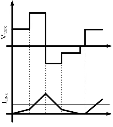
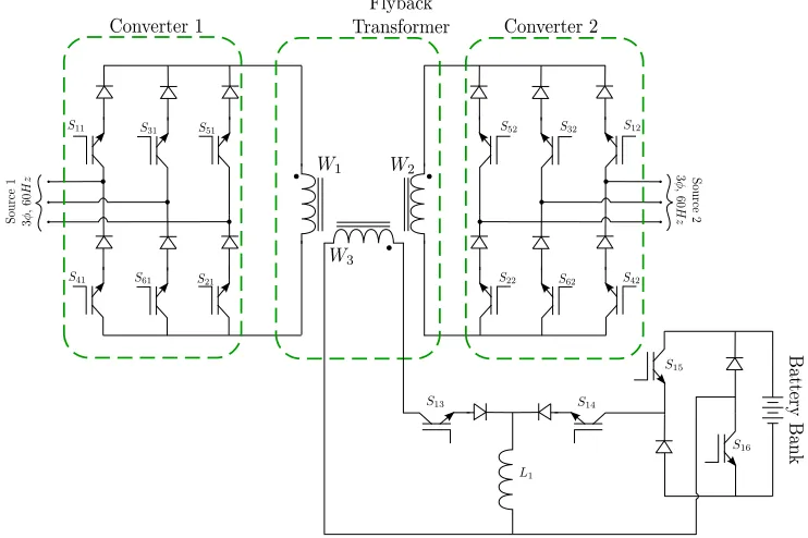
16 with two power conversion stages where each stage is comprised of a standard current-source converter [33]. Fig. 2.2 shows the circuit schematic of this converter. As it can be seen, the convertor consists of much fewer number of devices thereby reducing the overall loss, complexity and size of the system. Furthermore, input/output regulation can be achieved on a switching cycle-by-cycle across all the phases which results in a smaller passive component size. However, it should be noted that it is primarily a hard-switched converter. In one of the transition, a free-wheeling switch+diode leg is commuted which leads to significant amount of reverse recovery loss. Further, as the current in the link inductor needs to be nearly constant, a considerably large magnetic component is required for power transfer.
Figure 2.2: Circuit Schematic of Dyna-C.
The proposed controller forces a discontinuous mode of operation. This results in zero current turn on and turn off both at the starting and ending of the switching cycle. The switching scheme is so arranged that the series diode always turns off at zero voltage thereby reducing the reverse recovery losses and device stress. As the converter works under discontinuous mode, there are no freewheeling states. This further makes sure that the diode never undergoes forced reverse voltage commutation. Due to the inherent advantage of switch overlap, the turn on of all the switches (other than the first turn on which occurs at zero current), occur at zero voltage.
V
aV
bV
cV
o aV
o bV
o cS
1S
2S
3S
4T
1T
2T
3T
4S
5S
6T
517 These features result in overall lower device stress and high efficiency. As the inductor current follows a triangular trajectory, the value of inductance can be much lower as compared to conventional current source converters. A detailed principle of operation, simulation and hardware test results and a converter/device based comparison has been shown in the later sections.
This converter topology has also been modified to interface with battery to fit in UPS based applications. A cascaded version of this converter has been shown to connect to High Voltage applications. A sparse unidirectional rectifier topology has also been proposed which greatly reduces the number of active switches as compared to conventional converters.
2.2 Principle Of Operation
The principle of operation is explained in this subsection. For simplification, identical (in terms of voltage level and frequency) input and output grid is considered. For other cases, similar procedure can be used to achieve harmonic free power transfer without sacrificing any of the promised advantages. The operating condition is for unity power factor under balanced input and output voltages. This makes voltage and current bear a linear relation (eg. Va/Ia = Vb/Ib = Vc/Ic = constant). The input (and output) voltage/current waveform can be
divided into several 30° sectors.
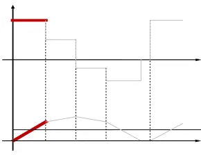
For this case, the sector where Va>0>Vc>Vb (which also means Ia>0>Ic>Ib) is studied as
18
Figure 2.3: Three Phase sinusoidal Input V-I waveform divided into six sectors where A=Red, B=Blue and C=Green. In this illustration, the current is leading the supply voltage.
The switching operation can be divided into five modes of operation:-
Mode 1: Starting from the input side, the link is connected to the input lines having the highest line-line voltage (Va-Vb in this case). To achieve this, S1, S4 and S6 are turned on. It
should be noted that even though S6 is turned on, it would not conduct as the series connected diode is reverse biased. The main motive of turning on S6 is to provide a necessary switch overlap which will be explained in the next mode of operation. With S1 and S4 turned on, the link is charged till the average value of one of the line current (Ib in this
case) is equal to the reference set by the controller. This turn-on duration can be calculated using the following formula: -
; where 'F' is the Switching Frequency of operation 1
2I Lb
t =
F(V - V )a b
19
Figure 2.4: Active Switches in Mode 1
Figure 2.5: Link Voltage and Current
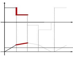
Mode 2: After the end of the previous mode, the switch S4 is turned off. The link inductor current now naturally starts flowing through S1 and S6. The fact that S6 was turned on much before (at the starting of Mode 1) it started conducting, this turn on occurs at near zero voltage. However, the turn-on loss is non-negligible for Si-IGBT [34]-[36]. SiC-MOSFET on the other hand shows a near zero loss in such transition. Further it should be noted that the turn off of series diodes of S4 are under zero voltage thereby reducing the reverse recovery current and stress. Switches T2 and T5 are also turned on (though it would not conduct as the series diodes are reverse biased) during this interval to facilitate zero voltage turn-on in the subsequent Mode. The turn-on duration of S1 and S6 in this mode is:-
Va Vb Vc Vo a Vo b Vo c
S1
S2 S3
S4
T1
T2 T3
T4 S5
S6
T5
T6
L
2 2(V -V )I
-b+ b +4aIc a b b (V -V )a c
t =2 ; where b= and a=
20
Figure 2.6: Active Switches in Mode 2
Figure 2.7: Link Voltage and Current
Figure 2.6 and Figure 2.7 shows the active switches (in red) and the corresponding link voltage and current waveforms.
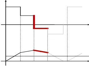
Mode 3: In this mode, the switches S1 and S6 are turned off. This forces the link current to flow through T2 and T5 (which were turned on in mode 2). This transition occurs under zero voltage condition thereby reducing the loss. The turn off of series connected diodes of S1 and S6 are under zero voltage. A negative voltage (Voc-Voa) appears across the inductor which
causes the link current to reduce linearly. The duration of turn on time of T2 and T5 is similar to the one mentioned in Mode 2 (the input voltage and current terms should be replaced by the appropriate output voltage and current). The switch T3 is also turned on in this duration (which would not conduct as the series diode is reversed biased). Fig. 2.8 and 2.9 shows the active switches (in red) and the corresponding link voltage and current waveforms.
Va Vb Vc Vo a Vo b Vo c
S1
S2 S3
S4
T1
T2 T3
T4 S5
S6
T5
T6
21
Figure 2.8: Active Switches in Mode 3
Figure 2.9: Link Voltage and Current
Mode 4: Switch T5 is turned off in this mode forcing the link current to flow through T2 and T3 (which was pre-turned on from the previous mode). This applies a negative voltage (Vb
-Va) across the link inductor causing the link current to further reduce linearly. At some point
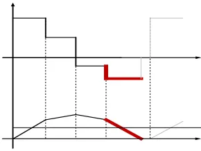
of time the current through the link will drop to zero. The series diodes of T2 and T3 will then naturally commute off to facilitate zero current turn off. This further reduces the overall losses on the converter. Fig. 2.10 and 2.11 shows the active switches (in red) and the corresponding link voltage and current waveforms.
Figure 2.10: Active Switches in Mode 4
Va Vb Vc Vo a Vo b Vo c
S1
S2 S3
S4
T1
T2 T3
T4 S5
S6
T5
T6
L
Va Vb Vc Vo a Vo b Vo c
S1
S2 S3
S4
T1
T2
T3
T4 S5
S6
T5
T6
22
Figure 2.11: Link Voltage and Current
Zero-Vector Mode: After the inductor current reaches zero value and all the switches are soft turned off, the system is allowed to rest till completion of switching time period. As this duration does not directly involve any power transfer, it is denoted as the zero-vector. This is similar to the free-wheeling stage of a conventional current source converter apart from the fact that both voltage and current in the inductor is zero during this mode for the proposed converter. Fig. 2.12 and 2.13 shows the circuit and waveforms during this Mode.
Figure 2.12: In Zero-Vector Mode, all switches are turned off
V
Li
nk
I
Li
nk
Figure 2.13: The Link voltage and current in Zero-Vector Mode
Va Vb Vc Vo a Vo b Vo c
S1
S2
S3
S4
T1
T2
T3
T4
S5
S6
T5
T6
23 These modes of operations are repeated thereby transferring power from the input supply to the output grid. In the proposed design, the value of inductor is kept relatively small. This increases the value of conduction dI/dt for the same input voltage level. This results in making the pulsating current triangular as compared to square shaped pulses (in the conventional control scheme) eventually enabling zero current switching.
2.3 Improvement in Reverse Recovery Current
Conventional DynaC and Constant Current Source based converters usually have an inherent issue of high reverse recovery stress. This occurs every switching cycle when the free-wheeling current (during zero-vector mode) flowing through the diode is forced commuted off. As the diode now has to block a significant reverse voltage, the peak reverse recovery current can be notably higher than the rated rms capability of the device [36]. Repeated high current stress operation can lead to device malfunction, unnecessary harmonics and EMI issues. The proposed converter provides a major advantage in this respect. The fact that during the zero-vector mode (when VLink = 0), the inductor current is zero owing to
discontinuous conduction mode. Therefore, instead of a free-wheeling state, there is a zero current state. As none of the diodes carry any current during this stage, when the circuit goes back to the power transfer mode, there is no reverse recovery.
24 this current. The diodes in this pole are hence conducting. After the completion of this mode when the power transfer mode (such as turning on S1+S4 like in mode 1) is reinstated, the conducting diodes are forced commuted off by a significantly large reverse voltage. As the value of reverse recovery current is a strong function of conduction current (in this case, it is approximately the DC current flowing through the switches and the inductor), characteristic di/dt of the switch and primarily the reverse blocking voltage, it exhibits a large negative peak current.
Figure 2.14: The Link voltage (top) and current (bottom) during zero vector mode of Conventional DynaC
25 This is not witnessed in Mode 1, 2, 3 and 4 as the voltage across diodes remained close to zero during turn off. This effectively reduced the reverse recovery stress. The aforementioned reverse recovery issue in conventional constant current source based converters is unavoidable. The only way to mitigate this phenomenon would be to replace regular Si-Diodes with SiC-JBS Si-Diodes with low reverse recovery losses. This however leads to significantly higher system cost. The inherent discontinuous mode operation in the proposed converter mitigates this problem completely. Fig. 2.15 shows the inductor voltage and current. During the zero-vector mode, the current through the inductor is zero. Hence, all the switches and diodes in the pole are not conducting. When the system shifts from zero-vector to Mode 1, the diodes do not exhibit any reverse recovery current as the conduction current was zero. This effectively lets the designer to use low cost PiN Diodes without the penalty of added switching loss. This also has far reaching consequence in the lifetime of these devices and effectively reduces unwanted harmonics and EMI associated with repeated operation of this.
2.4 Soft Switched Turn-Off Enabled By SiC-JBS Diode
As SiC-JBS Diodes exhibit low reverse recovery current and losses, forced commutation can be used to turn off the diodes before turning off the active switches. This pattern of operation is slightly different from the one mentioned in section 2. For simplicity the same sector where Va>0>Vc>Vb (which also means Ia>0>Ic>Ib) is studied like in Section 2. In this case,
26 turned off. Once the current through S6 is close to zero, the active switch can be turned off at zero current. This effectively reduces the turn off losses of the switches. As the reverse recovery current is low, the turn on loss of S4 is significantly low. This operation can be iterated during changeover from Mode 3 to 4 as well. The only hard turn off loss would occur during the transition from Mode 2 to 3 where the active switch has to be turned off to continue the power transfer operation.
Figure 2.16: The Link voltage and current for alternative control scheme
Fig. 2.16 shows the inductor voltage and current for this switching pattern. This algorithm should not be applied while using Si-PiN Diode as it exhibits large reverse recovery loss. It can be shown that overall efficiency of the converter is highly penalized when Si-PiN Diodes are used with this algorithm. It would be shown in the later section that the overall estimated efficiency of the converter with Si-PiN Diode (using the pattern discussed in Section II) is almost comparable to the one with SiC-JBS Diode (following the aforementioned pattern). As mentioned in the previous section, the price and availability of SiC-JBS Diodes at present
VL
IN
K
ILIN
27 are not comparable to Si-PiN Diodes. This makes Si-PiN the affordable and highly efficient choice for understudied converter.
2.5 System Dynamic Equations
In this section the dynamic equations of the system are derived. It is mentioned in the previous section that the inductor current has four sections in a periodic interval. The dynamic equations are derived for each of the intervals. In this case the source1 (connected to converter 1) is acting as a source of power and the source 2 (connected to converter 2) is acting as a sink of power.
The source 1 voltages are expressed as,
1 1 1
1 1 1
1 1 1
*sin( )
*sin( 2 / 3)
*sin( 2 / 3)
a m
b m
c m
v V t
v V t
v V t
Similarly, the source 2 voltages are expressed as,
2 2 2
2 2 2
2 2 2
*sin( )
*sin( 2 / 3 )
*sin( 2 / 3 )
a m v
b m v
c m v
v V t
v V t
v V t
Interval 1: The inductor current in this duration can be expressed as,
1 1 1 0 1 ( ) T
L a b
i v v dt
L
where, absolute value of all the voltages are considered.
It is mentioned earlier that in this duration, phase A and B of source 1 are conducting while the other phase is not. Therefore, this is the current expression for phase A and B (the direction of flow is not same).
28 1 1 0 1 a b v v I T L
The average value of A-phase current in a periodic interval (switching interval) is expressed as, 1 0 1, 2 a avg T I I T
For any given power factor angle θ1 in the converter 1 side we can write following expression,
1 0 1, 1 1sin( 1 1 1)
2
a avg m
T I
I k V T
T
where k1 is the scaling factor between voltage and current peak magnitudes, i.e., k1 = Im1/Vm1
Interval 2: In this duration, the phases B and C of the source 1 are the conducting phases and other phases are remaining idle. Similar to the earlier case, the inductor current can be expressed as (this is same as the absolute value of the phase B and phase C instantaneous currents),
2
1
1 1 1 1 0
1
| | | | ( )
T
L b c b c
T
i i i v v dt I
L
Let us denote the inductor current at the instant T2 as I1. So, 1 1
1 0 ( 2 1)
b c
v v
I I T T
L
The C-phase of the source 1 carries current only in this duration (in a switching cycle). So, the average C-phase current in a switching period can be expressed as,
2 1
1, (1 0)
2
c avg
T T
I I I
T