ABSTRACT
ZHANG, WENBO. Fast Volt - VAR Control on PV Dominated Distribution Systems. (Under the direction of Mesut E Baran).
Voltage Regulation is a fundamental operating requirement of all electric distribution
systems. Volt- VAR control aims at maintaining the voltages on a distribution feeder within
acceptable limits during all load conditions. PVs are becoming widely used in some
distribution systems. Since high penetration level of PV may adversely affect current
distribution system, steps must be taken to mitigate their impacts.
This thesis investigates the voltage issues of high penetration level of PV on traditional
power distribution systems and then proposes a new dynamic VAR compensator to address
and improve the system voltage performance. Dynamic VAR compensator is a new type of
Static VAR Compensator. The study involves simulating a prototype 34 node distribution
feeder with high penetration of PVs on PSCAD. Then, case studies have been conducted on
this system to investigate and demonstrate the volt –VAR issues on this system. The second
part of the thesis consists of case studies which investigates and assesses the use of DVC to
address the voltage regulation challenges on the prototype system.
The simulations show that DVC can help reduce operations of voltage regulator. If DVC
is used to replace all Volt – VAR control devices, it can provide a flatter voltage profile. In
PV dominated distribution system, DVC has a fast response to voltage change which can
prevent voltage drop caused by cloud. DVC can also help address high voltage violation in
high penetration level of PV. In summary, DVC could serve the voltage regulator and
© Copyright 2012 by Wenbo Zhang
Fast Volt - VAR Control on PV Dominated Distribution Systems
by Wenbo Zhang
A thesis submitted to the Graduate Faculty of North Carolina State University
in partial fulfillment of the requirements for the degree of
Master of Science
Electrical Engineering
Raleigh, North Carolina
2012
APPROVED BY:
_______________________________ ______________________________
Dr.Subhashish Bhattacharya Dr. Aranya Chakrabortty
BIOGRAPHY
Wenbo Zhang was born on July 27th 1988 in Dalian, Liaoning, China. She spent her early
childhood in Dalian, her hometown. And then she spent about three year finishing her
Bachelor of Engineering degree in Optical Engineering from Zhejiang University. In 2010,
she joined North Carolina State University to pursue Master of Science in Electrical
ACKNOWLEDGMENTS
I would like to acknowledge and deepest thank my advisor, Dr. Mesut E. Baran. He has
extensive knowledge in all areas of electrical engineering and accurate judgment, which
helps me find the direction and inspiration for my research in the past two years. Thank him
for the extra hours spent correcting my report and taking the time to tell me how to write an
excellent report. Thank him for teaching me how to think as an engineer and what do I need
to consider in a project. Thank him for his support throughout the time I was in NCSU.
I am grateful to my committee members, Dr. Subhashish Bhattacharya and Dr. Aranya
Chakrabortty for their time, valuable suggestions and help. And appreciate the assistance
from the staff members of FREEDM Systems Center.
It was a great pleasure to work with my partner Ankan De, who is a talent man and help
me a lot in the project. I learnt a lot from my friend Zhan Shen, who was my mentor and
taught me a lot. I am grateful to Thomas Nudell and Kyle Barth for their time and
suggestions on my thesis. I also want to thank all my friends’ help and support.
My heartfelt thanks my parents Qiujuan Wang and Peijie Zhang, whose love has always
TABLE OF CONTENTS
List of Tables ... vi
List of Figures ... vii
CHAPTER 1 INTRODUCTION ... 1
1.1 Background ... 1
1.1.1 Conventional Volt-VAR Control ... 2
a) Voltage Regulator Control... 5
b) Capacitor Bank Control ... 5
c) Coordination of VR and CAP ... 6
1.1.2 Photovoltaics ... 7
1.2 Proposed Approach ... 9
1.3 Organization ... 10
1.4 Glossary ... 10
CHAPTER 2 CONVENTIONAL VOLT-VAR CONTROL SCHEME ... 11
2.1 Prototype Feeder ... 11
2.1.1 Distribution Feeder Model ... 11
2.1.2 Component Models ... 12
2.2 Conventional Volt-VAR Control Study ... 16
CHAPTER 3 PV IMPACTS ON DISTRIBUTION SYSTEM ... 26
3.1 PV Impacts Studies ... 28
3.2 Case Studies ... 30
3.2.1 Case I ... 30
3.2.2 Case II ... 42
CHAPTER 4 DYNAMIC VAR COMPENSATOR... 53
4.1 Conventional System ... 57
4.1.1 Case 1: DVCs replace Voltage Regulators ... 57
4.1.2 Case 2: DVC at node 890... 66
4.1.3 Case 3: Three DVCs ... 72
4.2 DVC on system with PVs ... 76
4.2.1 Case 1: 2 DVCs ... 76
4.2.3 Case 3: 3 DVCs ... 89
4.2.4 Case 4: Two DVCs and PV under Cloud with static load ... 91
4.2.5 Case 5: One DVC and PV under Cloud with static load ... 94
4.2.6 Case 6: 3 DVCs and PV under Cloud with static load ... 97
4.2.7 Case 7: three DVCs and PV under Cloud with dynamic load ... 101
4.3 Flat Voltage ... 105
CHAPTER 5 SUMMARY AND FUTURE WORK ... 116
5.1 Summary ... 116
5.2 Future Work ... 117
REFERENCES ... 118
LIST OF TABLES
Table 1.1 Voltage range for 120V voltage level ... 2
Table 2.1 Feeder Voltage Device ... 12
Table 2.2 Voltage Regulator Parameters ... 15
Table 2.3 Tap Position ... 19
Table 3.1 PV systems placed on the prototype system ... 30
Table 3.2 numbers of operations of both Voltage Regulators ... 34
Table 4.1 Voltage Drop Comparison ... 60
Table 4.2 Voltage setting in DVCs ... 62
Table 4.3 Numbers of operations of two Voltage Regulators ... 71
Table 4.4 reactive power of DVCs at peak load ... 74
Table 4.5 Comparison of number of operations ... 87
LIST OF FIGURES
Figure 1.1 ANSI C84.1 Voltage range for 120V voltage level [1] ... 2
Figure 1.2 Traditional Distribution System ... 3
Figure 1.3 Without Volt-VAR Control under peak load ... 3
Figure 1.4 After raising the source voltage under peak load ... 4
Figure 1.5 Without Volt-VAR Control under light load after raising setting voltage ... 4
Figure 1.6 Voltage Regulators and Capacitor banks used on a distribution feeder ... 5
Figure 1.7 Voltage profile with voltage regulator and Capacitor [4] ... 6
Figure 1.8 Probability distributions of ten-minute-average voltages at all LV customer connection points in summer [8]... 8
Figure 1.9 Feeder Losses as a function of PV penetration level for two real distribution feeders [9] ... 9
Figure 2.1 Prototype System ... 11
Figure 2.2 Line-Drop Compensator circuit ... 13
Figure 2.3 VR control based on the set voltage, bandwidth and time delay... 14
Figure 2.4 Voltage Regulation Line Drop Compensator Circuit in PSCAD ... 14
Figure 2.5 Voltage Profile of no VRs at Peak Load ... 16
Figure 2.6 Voltage Profile with VRs at Peak Load ... 17
Figure 2.7 Voltage Profile comparison at Peak Load ... 18
Figure 2.8 Main Feeder Voltage Profile at Peak Load ... 19
Figure 2.9 Daily Load Profile at Node 856... 20
Figure 2.10 Voltage Profile at 10:30 AM ... 21
Figure 2.11 (a) Voltage Regulator 1 Tap Position (b) Voltage Regulator 2 Tap Position ... 22
Figure 2.12 Voltage Profile at 3:00 PM ... 23
Figure 2.13 Voltage Waveform at node 864 ... 24
Figure 2.14 Feeder Voltage Profile variation ... 25
Figure 3.1 Main components of a residential PV system ... 28
Figure 3.2 Normalized PV and Load profiles ... 31
Figure 3.3 Voltage waveform comparison of before and after PV installation at node 890 .. 32
Figure 3.4 Voltage profile comparison of before and after PV installation at 12:30 PM ... 33
Figure 3.5 (a)-(b) VR tap operation profile ... 35
Figure 3.6 Voltage Regulator Tap Number ... 37
Figure 3.7 Voltage Profile at Node 850 ... 38
Figure 3.8 Conventional VR ... 38
Figure 3.9 Power loss comparison ... 40
Figure 3.10 Power loss with PV installation ... 40
Figure 3.11 Voltage unbalance comparison at 12:30PM ... 41
Figure 3.12 PV power changes with sun irradiation ... 42
Figure 3.13 Voltage Profiles with cloud ... 43
Figure 3.14 Service voltage of Node 890 ... 44
Figure 3.15 Induction Motor in the system ... 45
Figure 3.17 Voltage Variation at node 860 ... 46
Figure 3.18 Voltage Variation at node 840 ... 47
Figure 3.19 Speed of Motors in the system ... 47
Figure 3.20 Motor Behavior at node 890 ... 48
Figure 3.21 Motor Behavior at node 860 ... 49
Figure 4.1 DVC installed in the grid ... 53
Figure 4.2 Circuit of Voltage Source Converter ... 54
Figure 4.3 DVC Model ... 54
Figure 4.4 DVC equivalent circuit ... 55
Figure 4.5 DVC Control Scheme ... 56
Figure 4.6 Voltage profile along the main feeder under peak load condition ... 57
Figure 4.7 Voltage Profile Comparison under peak load condition ... 58
Figure 4.8 Voltage Waveform Comparison at node 850 ... 59
Figure 4.9 Voltage Drop Waveform Comparisons ... 60
Figure 4.10 Reactive Power Profile of 2 DVCs ... 61
Figure 4.11 Power Loss Waveform Comparison ... 62
Figure 4.12 Voltage Profile under new setting condition at 7:30 PM (Peak Load)... 63
Figure 4.13 Q injections of two DVCs under new setting condition ... 64
Figure 4.14 Power Loss Waveform Comparisons under new setting condition... 65
Figure 4.15 Voltage Drop Comparison under new setting condition ... 65
Figure 4.16 Voltage Waveform at node 890 with closed loop control scheme ... 67
Figure 4.17 Voltage Profile under Peak Load Condition ... 68
Figure 4.18 Reactive Power Waveform of DVC ... 69
Figure 4.19 (a) – (b)Voltage Regulator Tap Position Comparison ... 70
Figure 4.20 Power Loss Waveform Comparison ... 71
Figure 4.21 Voltage Drop Comparisons ... 72
Figure 4.22 Voltage Profile for 3 DVC under Peak Load Condition (7:30PM) ... 73
Figure 4.23 Reactive Power Waveform of 3 DVCs ... 74
Figure 4.24 Power Loss Waveform Comparisons ... 75
Figure 4.25 Voltage Profile Comparison at 10:30 AM (high load) ... 76
Figure 4.26 Voltage Profile Comparisons at 12:30 PM (Peak PV) ... 77
Figure 4.27 Voltage Profile Comparison at 7:30 PM (Peak load) ... 78
Figure 4.28 Voltage Drop Comparisons ... 79
Figure 4.29 Reactive Power Profile Comparisons ... 80
Figure 4.30 Power Loss Waveform Comparisons ... 81
Figure 4.31 Power Loss Waveform Comparisons with lower voltage setting ... 82
Figure 4.32 Reactive Power Waveform Comparisons ... 82
Figure 4.33 Voltage Profile Comparisonswith new voltage setting at 12:30 PM (Peak PV) . 83 Figure 4.34 Voltage Drop Comparisons with new voltage setting ... 84
Figure 4.35 Voltage Profile Comparisons under Peak Load Condition ... 85
Figure 4.36 (a) – (b) Tap Position Comparisons... 86
Figure 4.37 Reactive Power Waveform of DVC ... 88
Figure 4.39 Voltage Profile at 7:30 PM (Peak Load) ... 89
Figure 4.40 Phase A Voltage Profile at 12:30 PM (Peak PV) ... 90
Figure 4.41 Reactive Power Waveform of 3 DVCs ... 90
Figure 4.42 Power Loss System Waveform ... 91
Figure 4.43 Voltage Profiles with cloud ... 92
Figure 4.44 Voltage Waveform at node 890 ... 93
Figure 4.45 Voltage Waveform at node 840 ... 94
Figure 4.46 Voltage Profile with Cloud ... 95
Figure 4.47 Voltage Waveform at node 890 ... 96
Figure 4.48 Voltage Waveform at node 840 ... 97
Figure 4.49 Voltage Profiles with DVC ... 98
Figure 4.50 Reactive Power Waveform ... 99
Figure 4.51 Voltage Waveform at node 890 ... 100
Figure 4.52 Voltage Waveform at node 840 ... 101
Figure 4.53 PV power changes with sun irradiation ... 102
Figure 4.54Voltage Waveform at node 890 with DVC ... 102
Figure 4.55 Voltage Waveform at node 860 with DVC ... 103
Figure 4.56 Voltage Waveform at node 840 with DVC ... 103
Figure 4.57 Motor Behavior at node 890 ... 104
Figure 4.58 Motor Behavior at node 860 ... 105
Figure 4.59 Prototype Feeder ... 108
Figure 4.60 (a)-(b) Voltage Waveform at node 840 and node 848 ... 109
Figure 4.61 Voltage Waveform at node 850 ... 110
Figure 4.62 Voltage Profile at 10:30 AM (High Load) ... 111
Figure 4.63 Voltage Profile at 3:00 PM (Light Load) ... 112
Figure 4.64 Voltage Profile at 7:30 PM (Peak Load) ... 113
Figure 4.65 Voltage Profile at 10:30 AM (High Load) ... 114
Figure 4.66 Voltage Profile at 3:00 PM (Light Load) ... 115
CHAPTER 1
INTRODUCTION
Voltage regulation is a fundamental operating requirement of all electric distribution systems. Volt-VAR control (VVC) aims to maintain the voltages on a distribution feeder within acceptable limits during all load conditions. In traditional systems, the most common VVC methods are direct voltage regulation and reactive power compensation. Voltage Regulators (VRs) and Capacitor Bank (CAPs) are conventional devices used in the distribution systems. VRs are typically placed at the substation and the CAPs are placed along the feeder.
1.1
Background
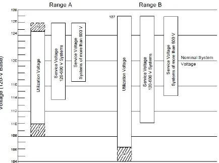
Figure 1.1 ANSI C84.1 Voltage range for 120V voltage level [1]
Table 1.1 Voltage range for 120V voltage level
Min Max Min Max
Range A (Normal) -5% 5% -8.30% 4.20% Range B(Emergency) -8.30% 5.80% -11.70% 5.80%
Service Utilization
1.1.1
Conventional Volt-VAR Control
Under heavy load conditions, the node farthest from the substation may have low-voltage violation (Figure 1.3). In order to fix this problem, we need to manually raise the source voltage (Figure 1.4), though this will cause other problems at light load (Figure 1.5). So Volt-VAR control is needed to deal with all possible normal operation conditions, [2].
Figure 1.2 Traditional Distribution System
Figure 1.3 Without Volt-VAR Control under peak load
Figure 1.4 After raising the source voltage under peak load
Figure 1.5 Without Volt-VAR Control under light load after raising setting voltage
local measurement based schemes. Figure 1.6 illustrates the typical application of these two kinds of devices.
Figure 1.6 Voltage Regulators and Capacitor banks used on a distribution feeder
a)
Voltage Regulator Control
VRs use local measurements of current and voltage to adjust the voltage at its terminals by changing its tap position. The VR is controlled by a VR relay and has two control options. The first option is regulating the voltage at its terminals. The second option is regulating a remote point down the feeder, which is achieved through a “line drop compensation” device that estimates voltage at the remote target point using voltage and current measurements,[3].
b)
Capacitor Bank Control
The reactive power of the load can be supplied by the substation or by capacitors. Installed capacitors can offset the reactive power demand of the load and consequently reduce the current and boost the voltage. Capacitors can be either fixed or switched. Fixed capacitors provide the minimum voltage boost needed during normal loading. Switched capacitors provide the extra voltage boost needed during heavy load conditions. Switched capacitors are thus switched off during light load conditions to prevent overvoltage conditions and to avoid power loss due to excessive reactive power compensation. Two main
switched in chunks, instead of varying continuously followed load demand. Second problem is as reactive power is a function of voltage squared, reactive power supplied by capacitors goes lower when the voltage is low, but that is when more reactive power is needed,[4].Usually very simple schemes are used to switch on or off the CAPs such as time of the day or voltage levels.
c)
Coordination of VR and CAP
One of the main challenges of local control schemes is the difficulty of coordinating the control between the VRs and CAPs. With the recent efforts towards extending SCADA at distribution feeder level, it is becoming possible to coordinate the operation of these devices. Figure 1.7 illustrates the voltage profile in a conventional system with voltage regulator and switched capacitor.
1.1.2
Photovoltaics
Recently, driven by raised average temperature and environmental destruction, Renewable Portfolio Standards (RPS) have been proposed in several countries [5]. Australia passed Renewable Energy (Electricity) Act in 2000. China proposed a renewable energy target in 2006 and modified it in 2009. The European Union adopted the Directive on Electricity Production from Renewable Energy sources in 2001. In America, many states have passed RPS programs with various different targets. For example, California’s target is to reach 33% of total power generation by 2020 and North Carolina’s target is 12.5% by 2021[5]. Right now wind, biomass and hydropower are the predominant resources used by most states to meet the requirement of RPS, while more and more states established a solar set-aside into the RPS, stipulating the percentage of energy from solar photovoltaics (PVs) at overall renewable energy. This kind of bills incentivizes the market for solar PVs, especially for grid-connected applications. Furthermore, most of the new PVs are installed in distributed grid and working as distributed generations. PVs are encouraged for environmental reasons, but we must note that PVs may adversely affect the existing distribution system. Utilities and power system operators need to consider the potential impact of high penetration levels of PVs on traditional distribution power systems and prepare robust measures to mitigate these impacts.
Traditional distribution systems were designed to operate in a radial fashion that supplies power from substation to loads, PV interconnections need to be studied to determine the potential impacts and propose more useful mitigation measures. PV has intermittent resource characteristic that varies the output power and requires inverters to convert dc to ac power, which may lead to more challenges given the volatile and uncontrollable nature of its primary resource,[6].
power flow, electric losses, power factor, and power quality. The effects vary in severity as a function of the penetration level and location of PV, [7].
Voltage rise leads to high voltage violation [8]. Based on BS EN 50160, which is the standard in Europe to gauge voltage acceptability, under normal operating conditions, all 10 minutes mean voltage should be less than 253V, while in Figure 1.8 for the 50% PV case, there is a probability of voltages exceeding 253V which is not acceptable, [9]. Figure 1.9 shows low and moderate penetration levels of PV may reduce power system losses but high penetration level of PV may lead to increase of power losses.
Figure 1.9 Feeder Losses as a function of PV penetration level for two real distribution feeders [9]
1.2
Proposed Approach
The aims of this thesis are to assess the impacts of high penetration levels of PV on conventional Volt-VAR control schemes in distribution system, and to investigate adopting a new dynamic VAR compensator for improving Volt-VAR control.
The study consists of the following steps:
1. Simulate a prototype traditional distribution system with conventional Volt-VAR control devices as the base case.
2. Assess impacts of high penetration levels of PV on the prototype system 3. Model and apply DVC on the prototype system
1.3
Organization
This thesis is organized as follows. In Chapter 2, conventional Volt-VAR control device for traditional distribution system is assessed. This establishes a base-case for the following chapters. Chapter 3 investigates the impact of integrating high penetration PV on the distribution system with traditional control devices. In Chapter 4, a new fast Volt-VAR compensator – Dynamic VAR Compensator is implemented in the system and its performance is assessed for both traditional system and the system with high PV penetration.
1.4
Glossary
PSCAD Power System Computer Aided Design is powerful simulation software. It has a powerful library of variable simulation model including electric machines, FACTS devices, transmission lines and cables.
PV Solar Photovoltaic
VR Voltage Regulator
DVC Dynamic VAR Compensator
CHAPTER 2
CONVENTIONAL VOLT-VAR
CONTROL SCHEME
The objective of this chapter is to investigate the effectiveness of conventional volt-VAR schemes outlined in Chapter 1. A prototype feeder is selected and implemented on PSCAD. The feeder’s primary circuit is modeled in detail, lines are represented in detail with equivalent circuits with mutual inductance terms, and loads are presented on a phase basis as constant impedances. This system will also be the base case for the following work.
2.1
Prototype Feeder
2.1.1
Distribution Feeder Model
IEEE 34 node test system is a traditional distribution system located in Arizona, composed of many unbalanced “distributed” and “spot” loads. This system was modeled on PSCAD. A single line diagram of the feeder is shown in Figure 2.1.
800
806 808 812 814
810 802 850 818 824 826 816 820 822
The system is radial and supplied by a medium-voltage transformer with a LTC installed. We assume the voltage at node 800 is constantly equal to 1.05 pu. The distribution system includes a main feeder and several laterals. There are 30 distributed loads and 6 spot loads ranging from 2 kW to 150 kW. The total load is 1769 kW. Fixed capacitors are installed at node 844 and node 848. The total rated reactive power injection is 750 kVAR. Two voltage regulators are installed, with one between nodes 814 and 850, and another between nodes 852 and 832 (Figure 2.1). The main feeder voltage is 24.9kV. A transformer is located between node 832 and node 888 steps down the primary voltage from 24.9 kV to 4.16kV.
2.1.2
Component Models
i) Primary circuit
There are 5 feeder configurations. Three of them are three-phase lines and the other two are single phase lines. One transformer and two capacitors are installed in the feeder. The parameters are shown in Table 2.1.
Table 2.1 Feeder Voltage Device
Type From To Rating
Transformer 832 888 500kVA
capacitor1 844 300kVAr
capacitor2 848 450kVAr
ii) Load
Loads were modeled as constant resistance loads (Np = Nq = 2). All loads are connected at the end of the line.
iii) Voltage Regulators
and current, and then calculates the voltage regulating point (VVRR) by transferring the measurements to a low-voltage circuit.
Figure 2.2 Line-Drop Compensator circuit
Voltage-regulating relay (VRR) is used to control tap changes. As illustrated in Figure 2.2, this relay has the following three basic settings that control tap changes:
• Setting voltage: The desired output of the regulator. It is also called the set point or band-center.
• Bandwidth (BW): Voltage regulator controls monitor the difference between the measured and the set voltages. Only when the difference exceeds one-half of the BW will a tap change start.
VRR compares the voltage VRR with the set point, if the difference between VRR and set voltage exceeds half of the BW, the timer starts counting. When the timer reaches TD, it sends a signal to move taps up or down.
Figure 2.3 VR control based on the set voltage, bandwidth and time delay
Figure 2.4 Voltage Regulation Line Drop Compensator Circuit in PSCAD Set
Voltage
TD
Tap-change
In this way, VRs calculate the voltage at a remote node by measuring local voltage and current and regulate the voltage to a preset reference voltage by changing the turn ratio of the transformer. In Figure 2.4, V and I represent local voltage and current measurements. Emeas represents the voltage of the regulating point and is used to determine how to change tap position. When there is reverse power flow in the grid, the current cross the impedance flows from right side to left side, so Emeas will be higher than Es. While under the normal power flow conditions, the current cross the impedance flows from the left side to the right side, so Emeas will lower than Es. Under both condition Emeas is presented the voltage of regulating point. So the LDC could work in bidirectional mode which ensures that VRs could work under reverse power flow when high penetration level PV installed in the system.
The VRs typically have 32 tap positions (±16) which correspond to a range of ±10% of transformer rated voltage. In other words, each step is 0.625% of the rated voltage. The tap changer is a mechanical device. Typically, the time needed to move from one position to the next is 1 – 2s. In large power systems, especially for those with long feeder systems, more than one VR is installed. An improper TD setting will result in unnecessary tap changes, which may shorten the life-time of the VR. The most common way to make them coordinated is to set a longer time delay for the VRs which are further from substation or are in lower voltage networks. The first VR’s time delay should be from 30 to 60s,[10], and further ones could range from 30 to 120s. The main parameters of VRs for the prototype system are listed in Table 2.2.
Table 2.2 Voltage Regulator Parameters
Location PT Ratio CT Rating Bandwidth Voltage Level R - setting X - setting
VR1 814 - 850 120 100 2 122 2.7 1.6
2.2
Conventional Volt-VAR Control Study
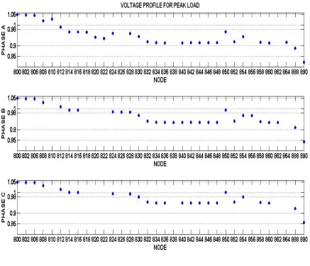
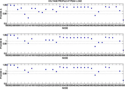
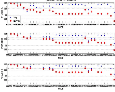
The simulation runs under peak load condition with no VRs in the system. Figure 2.5 shows the voltage profile. Most nodes are under low-voltage violation.
Figure 2.5 Voltage Profile of no VRs at Peak Load
limit (0.97 pu). Although voltage at node 890 was boosted from around 0.85pu to 0.94pu, it still has voltage violation which we will try to solve by using DVC and PV in the following chapters.
Figure 2.7 Voltage Profile comparison at Peak Load
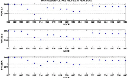
Figure 2.8 Main Feeder Voltage Profile at Peak Load
Table 2.3 Tap Position PHASE A PHASE B PHASE C
VR1 13 6 5
VR2 12 13 11
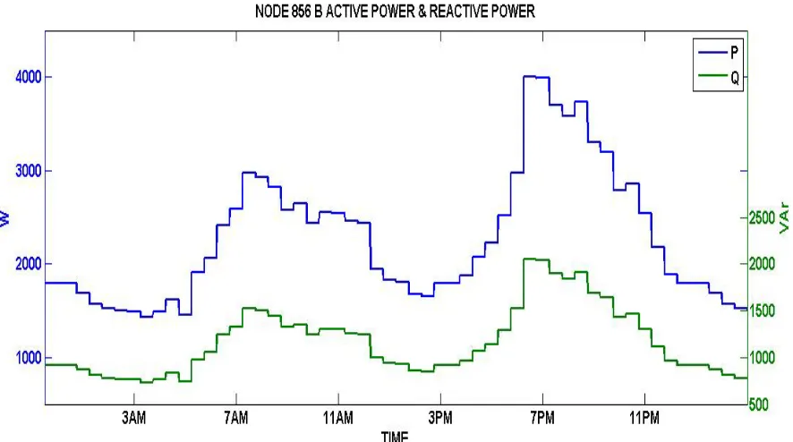
Figure 2.9 Daily Load Profile at Node 856
(a)
(b)
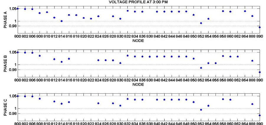
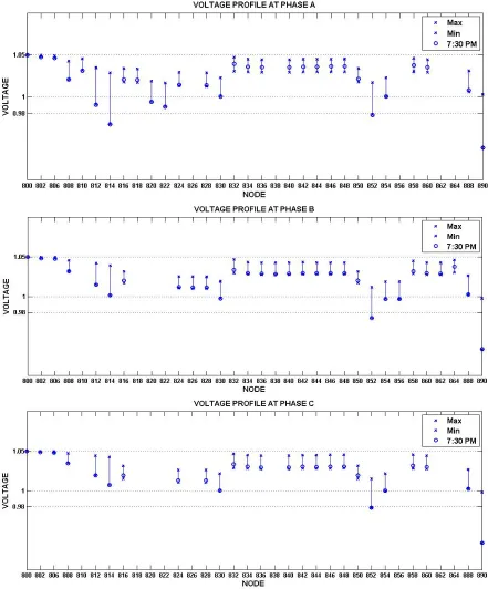
At 3:00PM the load demand is considered low and the voltage is relatively high. Figure 2.12 shows there is no low voltage violation in the system. The lowest voltage in the system is node 890 which is near 0.98pu. However there may be high voltage violation. In Figure 2.13, we clearly see the functionality of the automatic control scheme. When the voltage increase exceeds 1.05pu, the VRs will drop the tap position to drag the voltage back into the acceptable limits. In order to have a view of voltage changes during the whole day, Figure 2.14 shows the voltage profile range of each node.
CHAPTER 3
PV IMPACTS ON DISTRIBUTION
SYSTEM
The main goal of this chapter is to investigate the voltage related issues that arise when a considerable amount of distributed generation (DG) is installed on a distribution feeder. An increased amount of DG may have a significant impact on distribution system [5][6][7][8]. The main concerns identified involve reverse power flow, voltage rise, voltage unbalance, voltage fluctuation, improper VR operation, and increased power loss.
• Reverse power flow:
High penetration levels of PV can offset the feeder loads and the direction of power flow will be reversed from loads to neighbors or even to the substation. This situation is called reverse power flow. As distribution feeders are designed for unidirectional power flows, reverse power flow can negatively affect operation of line voltage regulators, particularly of the Line Drop Compensation (LDC), [11]. Furthermore, if substations have reverse power flow, the voltages and loading limits of some transformers may be affected.
• Voltage Rise:
• Voltage Fluctuations:
PV is an intermittent resource, therefore its varied output power lead to voltage variations which may cause power quality issues and complaints from customers. The severity of these voltage fluctuations must be assed to ensure that the system will not have voltage violation under any conditions.
• Voltage and current unbalance:
Single-phase high penetration PV may lead to significant voltage and current unbalance. For example, phase A has a PV installed and may experience reverse power flow, while phase B and phase C don’t have PVs and have normal power flow. However, PV can also provide active power to the load and offset unbalances between different phases. So if all three phases have PVs installed, the voltage and current unbalance will be mitigated.
• Interaction with voltage-controlled capacitor banks, LTCs, and line voltage regulators:
Voltage rise and fluctuations both can cause frequent operation of LTCs, line VRs and voltage-controlled capacitor banks. At noon, PV systems provide a large amount of power into the system, which boosts the voltage and the voltage regulators move down the tap position to maintain all of the voltage limits. When the sun sets, no power is supplied by the PV system, the voltage regulators need move up tap positions to keep the voltage within limits. The higher number of operations increases maintenance and shortens the life-cycle of the equipment. In addition, frequent operations in turn can augment voltage fluctuations and affect power quality. Furthermore, voltage fluctuations may affect the implementation of advanced Volt-VAR Optimization (VVO) schemes and Conservation Voltage Reduction (CVR) approaches.
• Power Losses
high penetration levels of PV, power system line losses tend to increase due to the reverse power flow which has larger magnitude of reverse direction currents. It is worth noting that these situations could happen within a single day. At noon, the load is light and the output of PV is maximal, so the line losses may increase. While during the late afternoon, the light isolation may decrease the penetration level of PV and decrease the power losses at the same time. Therefore we need to evaluate the average power losses instead of instantaneous losses. Voltage rise under high penetration levels of PV is also a reason to augment the high losses situation, because distribution transformer core losses are proportional to nodal voltage.
3.1
PV Impacts Studies
To investigate these issues, the prototype feeder shown in Figure 2.1 with detailed PV models is used. It is assumed that this is a residential feeder and some of the customers have installed photovoltaic (PV) systems on their rooftops. To simulate these PV systems, a typical grid connected PV system, shown in Figure 3.1, has been simulated. This system consists of a PV array with maximum power point tracking connected to a DC-DC converter and a DC-AC inverter to connect the system to the 240 AC supply. The model has been adopted from Colorado model [13].
The main objectives of the PV impact studies are to investigate steady-state and dynamic impacts previously discussed,[6]. The steady-state impact study is implemented by using distribution software analysis. The time-varied load and PV output are run with batch processes from which we determine the worst-case scenarios. The range of the time-varied data could be 8,760 hours of the year, 24 hours of the day, or half-hour intervals during a single day. The dynamic impacts study conducted with a more detailed model and simulating the worst-case scenarios identified in the steady-state study, [6].
A.
Steady-state impact study
Steady-state impact study can be conducted on both local and system-wide scopes [5]. Localized studies focus more on the impact of utility-scale PVs and mitigations on a specific feeder of a substation. System-wide studies address impacts of medium-scale or small-scale PVs on the overall utility power distribution systems, [6]. In these studies, the location, timeline and number of PVs are uncertain. Generally, studies may be targeted to comparing feeder voltage profiles, active and reactive power flows, distribution losses and operation of control devices (like LTCs, line voltage regulators and switched capacitors) before and after PV integration, [9]. These studies should be conducted over 8760 hours of the year to incorporate monthly and seasonal variation in load and PV generation. If this is not feasible due to the limitations of running time or data, a simplified study could be done for 30-min intervals over a 24 hour period.
B.
Dynamic-state impact study
3.2
Case Studies
Based on these guidelines, we developed two case studies for the PV impact study. Case I is focused on the steady- state impact of PV and normal operation of conventional Volt-VAR control devices. Case II is a cloud impact case study. Both static load and dynamic load will be used in the second case.
3.2.1 Case I
In this case, the main goal is to investigate the voltage-related issues that will happen when high penetration levels of PV system are installed in a distribution system. A modified prototype (Figure 2.1) is used.
It is assumed that five large load nodes on the feeder have installed PV systems. Table 3.1 shows the nodes and the size of the PVs at these nodes. Note that in this case it is assumed that PV capacity is about 70% of the maximum total load; hence, this case represents 70% PV penetration. Figure 3.2 shows the simulated power output profile of these PVs and the load profile during a day.
Table 3.1 PV systems placed on the prototype system
node 890 844 860 822 836
power 450 405 146 135 82
total percentage
Figure 3.2 Normalized PV and Load profiles
3.2.1.1 Voltage Rise
Figure 3.3 Voltage waveform comparison of before and after PV installation at node 890
Figure 3.4 shows the voltage profile along the entire feeder at noon, when PV power output is at maximum value. The voltages are flatter than when PVs are not installed. However, the voltages at node 812 and node 814 phase A suffer a high voltage violation. Voltage rise caused by PV system installation may lead to this high voltage violation problem.
1:00am 3:00am 5:00am 7:00am 9:00am 11:00am 1:00pm 3:00pm 5:00pm 7:00pm 9:00pm 11:00pm 0.9 0.95 0.98 1.05 NODE P H A S E B Voltage Rise WITH PV NO PV
1:00am 3:00am 5:00am 7:00am 9:00am 11:00am 1:00pm 3:00pm 5:00pm 7:00pm 9:00pm 11:00pm 0.9 0.95 0.98 1.05 NODE P H A S E B
Figure 3.4 Voltage profile comparison of before and after PV installation at 12:30 PM
800 802 806 808 810 812 814 816 818 820 822 824 826 828 830 832 834 836 838 840 842 844 846 848 850 852 854 856 858 860 862 864 888 890 0.98 1 1.05 NODE P H A S E A
VOLTAGE PROFILE @ 12:30 PM
800 802 806 808 810 812 814 816 818 820 822 824 826 828 830 832 834 836 838 840 842 844 846 848 850 852 854 856 858 860 862 864 888 890 0.98 1 1.05 NODE P H A S E B
3.2.1.2Interaction with line voltage regulators
a) Frequent operation
Voltage rise can cause frequent operation of line voltage regulators. Tap positions are shown in Figure 3.5. The number of operations is shown in Table 3.2. At noon, PV systems boost the voltage and the VRs need to lower the tap position to pull back the higher voltage. As the insolation decreases, the tap position increases. These increased movements increase the maintenance and shorten the life-cycle of VRs.
Table 3.2 numbers of operations of both Voltage Regulators
PHASE A PHASE B PHASE C PHASE A PHASE B PHASE C
NO PV 21 13 11 19 16 16
WITH PV 34 13 15 22 23 26
Raise
Percentage (%) 61.90 0 36.36 15.79 43.75 62.5
(a)
(b)
1:00am 3:00am 5:00am 7:00am 9:00am 11:00am 1:00pm 3:00pm 5:00pm 7:00pm 9:00pm 11:00pm -10-8 -6 -4 -20 2 4 6 8 10 TIME P H A S E A
VR1 TAP NUMBER
NO PV WITH PV
1:00am 3:00am 5:00am 7:00am 9:00am 11:00am 1:00pm 3:00pm 5:00pm 7:00pm 9:00pm 11:00pm -10-8 -6 -4 -20 2 4 6 8 10 TIME P H A S E B
1:00am 3:00am 5:00am 7:00am 9:00am 11:00am 1:00pm 3:00pm 5:00pm 7:00pm 9:00pm 11:00pm -10-8 -6 -4 -20 2 4 6 8 10 TIME P H A S E C
1:00am 3:00am 5:00am 7:00am 9:00am 11:00am 1:00pm 3:00pm 5:00pm 7:00pm 9:00pm 11:00pm -4 -20 2 4 6 8 10 12 14 TIME P H A S E A
VR2 TAP NUMBER
NO PV WITH PV
1:00am 3:00am 5:00am 7:00am 9:00am 11:00am 1:00pm 3:00pm 5:00pm 7:00pm 9:00pm 11:00pm -4 -20 2 4 6 8 10 12 14 TIME P H A S E B
b) Improper operation
Figure 3.7 Voltage Profile at Node 850
Figure 3.8 Conventional VR 814
850
Actualvoltage
850 calculated voltage
3.2.1.3 Power Loss
Figure 3.9 Power loss comparison
Figure 3.10 Power loss with PV installation
1:00am 3:00am 5:00am 7:00am 9:00am 11:00am 1:00pm 3:00pm 5:00pm 7:00pm 9:00pm 11:00pm 0.1
0.5 1 1.5
2x 10
5 NODE P L O S S POWER LOSS NO PV WITH PV
11:00am 12:00pm 1:00pm 2:00pm 3:00pm 1
1.1 1.2x 10
3.2.1.4 Voltage Unbalance
Three phase PV systems could improve the voltage unbalance. For each node, Equation (3-1) is used to calculate voltage unbalance.
𝑽(𝒖𝒏𝒃𝒂𝒏𝒍𝒂𝒏𝒄𝒆) = 𝑽𝒊𝒎𝒂𝒙− 𝑽𝒊𝒎𝒊𝒏 ( 3-1)
Where i represents Phase A, B or C. As Figure 3.11 shows, the maximum voltage difference between three phase decrease from 0.025pu to 0.0197pu and at most of the nodes, the voltage difference decreases slightly.
Figure 3.11 Voltage unbalance comparison at 12:30PM
𝑉(𝑢𝑛𝑏
𝑎𝑛𝑙𝑎
𝑛𝑐
3.2.2 Case II
3.2.2.1 Cloud Impact with Static Load
As we mentioned before, the tap position in the voltage regulator is kept in a relatively low position at noon. If clouds sweep over this network within a short period of time, PV power contribution will drop quickly. Although the VR can observe a voltage decrease, the LTC controller will not response immediately due to time delay, so the voltage drop will remain for a short time. Because the voltage drop is a function of distance from the substation, the voltages at some remote nodes may have already suffered unacceptably low voltage.
The cloud transient is simulated by a decrease in solar irradiation from 1000 to 70 W/m2 over a 20s period of time from 80 to 100s as shown in Figure 3.12,[10].The PV active power output follows the solar radiation.
Figure 3.13 show the voltage profile for the cloud impact. In this case, phase A has the worst voltage profile and the voltage at node 890 is most severely affected by cloud coverage. Figure 3.14 shows the voltage profile at node 890. Following cloud cover, the voltage at node 890 drop down to 0.89 pu which exceeds the low-voltage limits for 15s and then comes back within limits after 30s.
3.2.2.2 Cloud Impact with Dynamic Load
a) 70% penetration
In this case, dynamic load models are implemented in the simulation. We adopt 50% resistive loads and 50% small induction motor loads in the system. A squirrel cage induction machine (shown in Figure 3.15) is implemented as a dynamic load. The loading torque is assumed to be about 0.45 pu at noon and the stalling voltage is around 0.95pu. When one motor starts to stall, it will draw more current, which may cause a lower voltage. But after the speed goes down to zero, the motor will be disconnected from the grid and the total load will decrease, which may lead a voltage jump in the grid.
Figure 3.15 Induction Motor in the system
Figure 3.16 Voltage Variation at node 890
Figure 3.18 Voltage Variation at node 840
From Figure 3.19, we can see that motor 890 begins to stall at 12s and motor 844 begins to stall at around 20s. Although the other two motors have a very low speed at 22s, they do not stall and the speeds of these two motors come back to normal after voltage regulator acts.
Figure 3.20 – Figure 3.21 show more clearly the behavior of induction motors in the simulation. At around 15s the motor at node 890 stops, which means the residential device stops working because of cloud cover. This serious problem will cause custom complaints. So in the following chapter, we attempt to use DVC to maintain the voltage and keep the all the motors working during cloud cover.
Figure 3.21 Motor Behavior at node 860
b) Low Penetration (5%)
In the previous section, with 70% penetration of PV, two motors stop working during cloud cover. That proves that high penetration level of PV can cause induction motor stall. This case is to determine the maximum PV penetration which will not affect the induction motor working.
Table 3.3 PV systems placed on the prototype system
node 890 844 860 822 836
power(kW) 22.5 40.5 14.6 6.75 8.2 total (kW)
percentage
92.55 5%
Table 3.4 VR2 Tap Position under Different PV Penetration Phase A Phase B Phase C
30% 6 6 4
10% 7 7 4
5% 7 7 5
No PV 7 9 6
Table 3.5 Voltage Comparison at node 890 after cloud covers all of the PVs
Phase A Phase B Phase C
30% 3175 3170 3172
10% 3197 3202 3202
5% 3269 3255 3272
No PV 3295 3298 3300
CHAPTER 4
DYNAMIC VAR COMPENSATOR
As shown in the previous chapter, voltage problems like high voltage violation or frequent operation of control devices caused by high penetration level of PV needs some viable solution. Dynamic VAR Compensator is a new type of Static VAR Compensator, with its own advantages. Usually, DVC is smooth and can continuously adjust reactive power [12],[14]. DVC can help solve the reactive compensation problem for many different transmission or distribution applications. Figure 4.1 illustrates the usual place where DVC installed, which is similar to capacitors. In this work, DVC is used to address voltage problems in a distribution system.
Figure 4.1 DVC installed in the grid
Figure 4.3 shows the model used in this thesis. The DC output voltage and voltage on the grid are two input reference of controller. The controller calculates three phase voltage and sends it back to the three phase controlled voltage sources.
Figure 4.2 Circuit of Voltage Source Converter
Input Filter PQ Loss LUT IABC VABC VA VB VC PQ VDC Constant Power Load Controller Qref VABC ref
Figure 4.3 DVC Average Model
𝑉𝐴
𝑉𝑑𝑐
Figure 4.4 shows an equivalent DVC model in PSCAD, this model is made by Ankan De[15]. RYB is represented as an electric node which is connected to grid. A control signal is sent by the DVC controller to a1, a2 and a3. The controller is shown in Figure 4.5.
Figure 4.4 DVC equivalent circuit
Figure 4.5 DVC Control Scheme
Case Studies
The goal is to investigate the DVC’s performance when used as a Volt-VAR control device in the distribution system, and to determine whether it can help address the voltage problem in the system with a high penetration of PV. First, we integrate DVC into the conventional system to see whether it can replace voltage regulators and capacitors. Second, we use it in the system with high penetration of PV to see whether it can address the problem caused by the PV. Lastly, we use DVC to achieve flat voltage function to prepare a flatter voltage profile, which is required for Conservation Voltage Reduction.
4.1 Conventional System
4.1.1 Case 1: DVCs replace Voltage Regulators
In this case, we use DVC to replace two voltage regulators (at 814 and 852). With a line drop compensator integrated, VRs regulate two remote nodes, which are located around node 850 and node 832. Thus we put DVCs at node 850 and node 832 to verify whether they can realize the functionality of voltage regulators.
Three-phase DVCs can only regulate one phase voltage at a preset value. In this case, the DVC regulates voltage at phase A. The reason is phase A has the lowest voltage among the three phases and if we regulate a different phase, the lateral connected to phase A (node 818, 820 and 822) will suffer a low voltage violation. From the Figure 4.7, we can see that at node 832 and 850, both VRs and DVCs boost the voltage to a preset value. As we mentioned in base case, voltage at node 814 and node 852 which are the nodes just in front of the voltage regulator, have a low voltage violation. As there is no load connected to these notes, this is not of much concern. But this is a disadvantage of using the VRs. However, DVC avoids this disadvantage and gives us a flatter voltage profile.
Figure 4.7 shows the voltage profile for every node under peak load condition. It shows us that node 890 still has a voltage violation issue. Figure 4.8 shows the comparison of voltage waveforms at node 850 where the DVC is located. The DVC can regulate the voltage exactly equal to a preset value, while the VR can only regulate the voltage within a small range.
Figure 4.8 Voltage Waveform Comparison at node 850
In order to quantify how well DVC helps flatten the voltage, we need to check the voltage drop (VD) along the feeder at the nodes where loads are connected.
𝑽𝑫 = (𝑽𝒍𝒐𝒂𝒅)𝒎𝒂𝒙− (𝑽𝒍𝒐𝒂𝒅)𝒎𝒊𝒏 ( 4-1)
Figure 4.9 Voltage Drop Waveform Comparisons
Table 4.1 Voltage Drop Comparison
PHASE A (P.U) PHASE B (P.U) PHASE C (P.U)
BASE 0.068 0.056 0.057
Figure 4.10 Reactive Power Profile of 2 DVCs
Figure 4.11 Power Loss Waveform Comparison
Figure 4.11 shows the power loss comparison. As the Q injection of DVC is too large and it already exceeds the Q requirement of the system. Thus the power loss in the system is much higher than the base case. As the voltage drop along the feeder reduces, we could lower the voltage setting in the DVC to reduce the power loss. As shown in Figure 4.7, there is a lateral node 818 - node 822 connected in phase A which has the lowest voltage (around 0.98pu) so we cannot lower the first DVC’s setting. For the second DVC, we could reduce the setting by 0.045pu. The new settings of two DVCs are shown in Table 4.2.
Table 4.2 Voltage setting in DVCs
Figure 4.12 Voltage Profile under new setting condition at 7:30 PM (Peak Load)
The voltage profile with new voltage setting in the DVC is shown in Figure 4.12. Although the setting of second DVC drops down, the voltages at load connected node except node 890 are all within acceptable limits.
MW to 0.22 MW. However, the voltage drop (shown in Figure 4.15) increases during light load condition, slightly decreases in the heavy load condition.
Figure 4.14 Power Loss Waveform Comparisons under new setting condition
Our goal is to maintain all of the voltages within limit. Both settings could achieve this goal. With second settings, we can minimize system power loss, but the system has slightly larger voltage drop along the feeder. In other words, we could decrease the reference in DVC to a relatively lower value to reduce power loss in the system, as long as all the voltages at load connected nodes are within the limits.
4.1.2 Case 2: DVC at node 890
In this case, DVC is used to fix the low voltage violation at node 890 and eliminate the tow capacitors in the system. As we mentioned in the base case, node 890 has the worst case of voltage violation, so we integrate DVC at node 890 to see whether it can help address the voltage issue and maintain all the voltage within acceptable limits. We also remove the capacitors at node 844 and node 848 to see whether DVC will still maintain the voltages.
Figure 4.16 Voltage Waveform at node 890 with closed loop control scheme
Figure 4.17 Voltage Profile under Peak Load Condition
Figure 4.18 Reactive Power Waveform of DVC
(a)
(b)
Table 4.3 Numbers of operations of two Voltage Regulators
CAP DVC CAP DVC CAP DVC
VR1 23 22 13 8 11 11
VR2 14 16 24 8 16 11
PHASE A PHASE B PHASE C
Figure 4.20 shows the power loss in the system. The voltage in this case is higher than base case, so the power loss is also higher than base case. As DVC solves the low voltage issue, the voltage drop improves a little (Figure 4.21).
Figure 4.21 Voltage Drop Comparisons
4.1.3 Case 3: Three DVCs
Based on the previous two cases, we consider using three DVCs in the system to replace all of the conventional Volt-Var control devices. In this case, we replace the two VRs at node 814 and node 852 and the capacitors at node 844 and node 848 with three DVCs located at node 850, node 832 and node 890.
Figure 4.22 Voltage Profile for 3 DVC under Peak Load Condition (7:30PM)
Figure 4.23 Reactive Power Waveform of 3 DVCs
Table 4.4 reactive power of DVCs at peak load DVC @ 850
(MVAR)
DVC @832 (MVAR)
DVC @ 890 (MVAR)
Case 1 0.68 0.63
Case 2 0.45
Case 3 0.65 1 0.61
0.99 pu. So DVC needs to provide more reactive power to boost the voltage in Case3. Comparing Case 1 and Case3, adding the third DVC could slightly reduce the size of the previous DVCs. As DVC at node 890 eliminates the two capacitors in the system, the other two DVC should provide more reactive power to compensate the reactive power provided by capacitors in the base case.
Figure 4.24 shows the power loss comparisons of base case and Case 3 with three DVCs. As the voltages in DVC case are higher than base case, the power loss is also higher.
Figure 4.24 Power Loss Waveform Comparisons
4.2 DVC on system with PVs
4.2.1 Case 1: 2 DVCs
With PVs integrated into the system, we will determine how DVCs can address the problems discussed in Chapter 3.
Figure 4.25–Figure 4.27 show the comparison of the system voltage profile at three different point of time: 10:30 AM (high load), 12:30 PM (Peak PV output) and 7:30 PM (Peak load).
Figure 4.27 Voltage Profile Comparison at 7:30 PM (Peak load)
As Figure 4.26 shows, with PV integrated, the voltages gave high voltage violation, while after using DVCs instead of VRs in the system, the voltages all stay within the acceptable limits. Thus the voltage rise problem could be solved with DVC.
Figure 4.29 Reactive Power Profile Comparisons
Figure 4.30 Power Loss Waveform Comparisons
Figure 4.31 Power Loss Waveform Comparisons with lower voltage setting
Figure 4.34 Voltage Drop Comparisons with new voltage setting
4.2.2 Case 2:1 DVC at node 890
This case shows how DVC helps improve the frequent operations problem caused by PV integration and solves the low voltage violation at node 890 at night.
Figure 4.35 Voltage Profile Comparisons under Peak Load Condition
(a)
Table 4.5 Comparison of number of operations
VR1 VR2
BASE 20 21
PV 34 25
DVC 31 25
BASE 13 16
PV 13 23
DVC 10 17
BASE 11 16
PV 15 26
DVC 12 18
PHASE A
PHASE B
PHASE C
Figure 4.37 Reactive Power Waveform of DVC
Figure 4.38 shows the power loss waveform comparisons. DVC will increase the power loss, but as PVs reduce losses a lot in the day time, the power losses in the day time are still lower than the base case, while at night, the losses are higher than the base case.
4.2.3 Case 3: 3 DVCs
Combining Test Case 4 and Test Case 5 and we construct a system with three DVCs and 70% PV penetration. Figure 4.39 shows the voltage profile under peak load condition. All of the voltages are within acceptable limits. Figure 4.40 shows the voltage profile at phase A at noon (peak PV). In this figure, adding DVC in the system fixes the high voltage violation problem.
Figure 4.40 Phase A Voltage Profile at 12:30 PM (Peak PV)
Figure 4.41 Reactive Power Waveform of 3 DVCs
about 1 MVAR at night. The DVC at node 890 generates about 0.61 MVAR at night. Figure 4.42shows the power loss system waveform.
Figure 4.42 Power Loss System Waveform
4.2.4 Case 4: Two DVCs and PV under Cloud with static load
In this case, the goal is to investigate the performance of DVCs under cloudy conditions and to compare it with the performance of conventional devices. We integrate two DVCs into the system. They are used to replace traditional VRs. The cloud transient is simulated as in Chapter 3. PVs also have the same output power as in the base case.
Figure 4.44 Voltage Waveform at node 890
Figure 4.44 shows the voltage waveform at node 890 which has low voltage violation. When clouds begin passing over the PVs, the voltage at node 890 drops, and when all the PVs are covered by the cloud, the voltage is about 0.96 pu.
Figure 4.45 Voltage Waveform at node 840
4.2.5 Case 5: One DVC and PV under Cloud with static load
In this case, only one DVC is integrated in the system at node 890. It used to fix the voltage problem and eliminate capacitors.
Figure 4.46 Voltage Profile with Cloud
Figure 4.48 Voltage Waveform at node 840
4.2.6 Case 6: 3 DVCs and PV under Cloud with static load
Figure 4.49 Voltage Profiles with DVC
Figure 4.52 Voltage Waveform at node 840
Figure 4.51 shows the voltage waveform at node 890. Figure 4.52 shows the voltage waveform at node 840. As we can see, neither voltage varies with as PV output decreases. So using DVC instead of VR in systems with high penetration of PV could help solve the voltage problem caused by clouds.
4.2.7 Case 7: three DVCs and PV under Cloud with dynamic load
Figure 4.53 PV power changes with sun irradiation
Compared to the large voltage drop from the PV panels after cloud cover in the system without DVC (Figure 3.16, Figure 3.18), voltages in this case with the DVCs doesn’t change much. The result is that the motors all work well and do not stall.
Figure 4.55 Voltage Waveform at node 860 with DVC
Figure 4.56 Voltage Waveform at node 840 with DVC
Figure 4.58 Motor Behavior at node 860
4.3 Flat Voltage
Snohomish PUD, the customer could save 281 kWh / yr with a net bill reduction of $6.28 / yr[18]. So Implementing CVR can be a good way for utilities to save energy.
If the system has a heavy load feeder or a long feeder, which means the voltage at the end of the feeder are only slightly higher than the lower limits, then the utilities cannot reduce substation voltage. Thus a relatively flat voltage profile is required for implementing CVR. In the conventional system, VR with line-drop compensation and capacitors are often used to keep voltage flat along the feeder [17][19]. In our study, we will use DVC to get a flat voltage profile and a future study could be done to implement CRV to save energy.
The objective of this study is to make the voltage profile flat. Five DVCs were installed in the system to realize this goal. The source voltage is set to 1.0pu. From the previous study, we found that the lowest voltage among three phases is phase A, so in this study phase A is regulated. Another reason to regulator phase A is that there is a lateral in phase A (Node 816, 818, 820, 822) which has a large load connected to it. If we regulate other phases, like phase B, node 822 will have voltage violation.
There are two algorithms to determine optimal placement of VRs in distribution system. The first algorithm uses candidate buses where the VRs are located. After adding VRs at these buses, it is needed to reduce the number of VRs based on economic aspects and objective of placing VR. The second algorithm first finds violation buses and computes the distance from these buses to the substation. It places a VR at the nearest bus. New violation buses are found, and processes is repeated until no violation bus existed, [20][21].
buses. Table 4.6 shows the voltages in the system with three DVCs under peak load condition.
Table 4.6 Voltage with three DVCs under peak load condition
NODE PHASE A PHASE B PHASE C NODE PHASE A PHASE B PHASE C
800 1 1 1 836 0.9922 1.00648 1.00439
802 0.99947 0.99969 0.99965 838 0 1.00601 0 806 0.99913 0.99949 0.99944 840 0.99217 1.00643 1.00436 808 0.99474 0.99996 0.99907 842 0.99295 1.00729 1.00499 810 0 0.99966 0 844 0.99248 1.00669 1.00451 812 0.99528 1.00689 1.00443 846 0.99234 1.0061 1.00427 814 0.99996 1.01633 1.01327 848 0.99232 1.00605 1.00426 816 0.99978 1.01626 1.0132 850 0.99996 1.01633 1.01327 818 0.99887 0 0 852 0.99996 1.01508 1.01187 820 0.97328 0 0 854 0.99606 1.01164 1.00903
822 0.96744 0 0 856 0 1.01134 0
824 0.99801 1.01349 1.01135 858 0.99676 1.01156 1.00875
826 0 1.0131 0 860 0.99249 1.00692 1.0046
Figure 4.59 Prototype Feeder
Table 4.6, the nodes in the circles have low voltage and the lowest voltage is 0.992 pu. The nearest node in this case is node 834, so we add another DVC at node 834 to improve the voltage profile. Figure 4.60 - Figure 4.61 show the voltage waveforms at node 840 which is at the end of the main feeder and node 850 which has a DVC connected. From the figures, we see that voltages at phase A are kept at 1 pu which indicates that using DVCs could perfectly achieve the goal of keeping the voltages equal to 1 pu.
800
806 808 812 814
810 802 850 818 824 826 816 820 822
828 830 854 856
(a)
(b)
Figure 4.61 Voltage Waveform at node 850
Figure 4.64 Voltage Profile at 7:30 PM (Peak Load)
Figure 4.66 Voltage Profile at 3:00 PM (Light Load)
CHAPTER 5
SUMMARY AND FUTURE WORK
5.1 Summary
High penetration of PV leads to high voltage violation and reverse power flow. It also causes increased operations and abnormal operation of conventional VRs. Although small and medium penetration level of PV could help reduce power losses in the system, high penetration level of PV may increase the power losses in the system. Under cloudy conditions, VRs cannot response to the fast voltage drop which may result in an unstable situation. If there are dynamic loads like motors in the system, low voltage may cause the device stopping working, which may lead to customer’ complaints.
Facing these problems, we proposed to use DVC to replace conventional volt-VAR control devices. Based on the results from the case studies, DVC could completely realize the functionality of VRs and capacitors in a distribution system. Furthermore, DVC has better performance on the following aspects:
• When DVC is used to replace capacitors as in 4.1.2 case 2, it can help reduce the number of operations of VRs, which could help reduce the maintenance fee and increase the life time of these devices.
• As in 4.1.1 case 1 illustrates, DVC can provide a flatter voltage profile than conventional volt-VAR control devices. In 4.3, using more DVCs could maintain all the voltage within range 0.99pu to 0.01pu which could not achieve by conventional devices.
DVC also performs well while addressing the problems caused by high PV penetration.
• As in 4.2.2 case 2 illustrates, DVC can solve the frequent operations of VR problem by maintaining the voltage at all times regardless of PV output..
• In both 4.2.4 and 4.2.5, DVC provides a fast response to voltage change which ensures voltage within acceptable limit under all conditions.
5.2 Future Work
REFERENCES
[1] ANSI C84.1, Electric Power Systems And Equipment – Voltage Ratings (60 Hertz), April 2011
[2] B. Uluski, “Approaches to Volt-VAR Control and Optimization”, Transporting You into the 21st Century Distribution System, September 16, 2010.
[3] TuranGonen, Electric Power Distribution System Engineering, McGraw-Hill, 1986.
[4] E. Liu, J. Bebic, “Distribution System Voltage Performance Analysis for High-Penetration Photovoltaics” GE Global Research Niskayuna, New York, Subcontract Report, NREL/SR-581-42298, February 2008
[5] http://www.dsireusa.org/incentives/index.cfm?SearchType=RPS&&EE=0&RE=1, DSIRE Database of State Incentives for Renewables & Efficiency
[6] FaridKatiraei, Julio Romero Aguero, ”Solar PV Integration Challenges”, IEEE power & energy magazine, May/June 2011
[7] Miroslav M. Begovic, I. kim, D. Novosel, J. Romero Agüero, A. Rohatgi,”Integration of Photovoltaic Distributed Generation in the Power Distribution Grid”, 45th Hawaii International Conference on System Sciences 2012
![Figure 1.7 Voltage profile with voltage regulator and Capacitor[4]](https://thumb-us.123doks.com/thumbv2/123dok_us/1454155.1178168/17.612.103.513.354.654/figure-voltage-profile-voltage-regulator-capacitor.webp)
![Figure 1.8 Probability distributions of ten-minute-average voltages at all LV customer connection points in summer[8]](https://thumb-us.123doks.com/thumbv2/123dok_us/1454155.1178168/19.612.117.520.263.509/figure-probability-distributions-minute-average-voltages-customer-connection.webp)