University of Windsor University of Windsor
Scholarship at UWindsor
Scholarship at UWindsor
Electronic Theses and Dissertations Theses, Dissertations, and Major Papers
2018
SYSTEM-ON-A-CHIP (SOC)-BASED HARDWARE ACCELERATION
SYSTEM-ON-A-CHIP (SOC)-BASED HARDWARE ACCELERATION
FOR HUMAN ACTION RECOGNITION WITH CORE COMPONENTS
FOR HUMAN ACTION RECOGNITION WITH CORE COMPONENTS
Amin Safaei
University of Windsor
Follow this and additional works at: https://scholar.uwindsor.ca/etd
Part of the Electrical and Computer Engineering Commons
Recommended Citation Recommended Citation
Safaei, Amin, "SYSTEM-ON-A-CHIP (SOC)-BASED HARDWARE ACCELERATION FOR HUMAN ACTION RECOGNITION WITH CORE COMPONENTS" (2018). Electronic Theses and Dissertations. 7666.
https://scholar.uwindsor.ca/etd/7666
SYSTEM-ON-A-CHIP (SOC)-BASED HARDWARE ACCELERATION FOR HUMAN ACTION RECOGNITION WITH CORE COMPONENTS
by
Amin Safaei
A Dissertation
Submitted to the Faculty of Graduate Studies
through the Department of Electrical and Computer Engineering in Partial Fulfillment of the Requirements for
the Degree of Doctor of Philosophy at the University of Windsor
Windsor, Ontario, Canada
System-on-a-chip (SoC)-based hardware Acceleration for Human Action Recognition with Core Components
by
Amin Safaei
APPROVED BY:
W. Shen, External Examiner University of Western Ontario
D. Wu
School of Computer Science
M. Ahmadi
Department of Electrical and Computer Engineering
E. Abdel-Raheem
Department of Electrical and Computer Engineering
Dr. Q. M. J. Wu, Advisor
Department of Electrical and Computer Engineering
Declaration of Co-Authorship / Previous
Publication
I. Co-Authorship Declaration
I hereby declare that this dissertation incorporates material that is result of joint
research, as follows: This dissertation incorporates the outcomes of joint research
undertaken in collaboration with Dr. Yimin Yang and Mr. Thangarajah Akilan
under the supervision of professor Jonathan Wu.
The collaboration is covered through Chapters 3, 4, 5 and 6 of the dissertation. In
all cases, the key ideas, primary contributions, experimental designs, data analysis and
interpretation, were performed by the author, and the contribution of the collaborator
was primarily through the provision of valuable suggestions for the representation of
ideas, for the analysis of the results for the experiments carried out and editorial
activities throughout the process of dissemination of the work.
I am aware of the University of Windsor Senate Policy on Authorship and I certify
that I have properly acknowledged the contribution of other researchers to my
disser-tation, and have obtained written permission from the only co-author to include the
above material in my dissertation.
I certify that, with the above qualification, this dissertation, and the research to
which it refers, is the product of my own work.
II. Declaration of Previous Publication
This thesis includes 4 original papers that have been previously published/submitted
thesis Chapter Publication title/full citation Publication status Chapter 3 A. Safaei and Q. M. J. Wu, Y. Yang,
”System-on-a-chip (SoC)-based hardware acceleration for foreground and background identification,” Jour-nal of the Franklin Institute, Volume 355, Issue 4, 2018, Pages 1888-1912 c2017 The Franklin Insti-tute.Reprinted, with permission,
published
Chapter 4 A. Safaei, Q. M. J. Wu and T. Akilan, ”System-on-chip-based hardware acceleration for human de-tection in 2D/3D scenes,” 2017 IEEE Interna-tional Conference on Systems, Man, and Cybernet-ics (SMC), Banff, AB, 2017, pp. 1041-1045. c2018 IEEE.Reprinted, with permission
published
Chapter 5 A. Safaei and Q. M. J. Wu, ”System-level design for human action recognition in 3D scenes,” 2017 IEEE International Conference on Systems, Man, and Cybernetics (SMC), Banff, AB, 2017, pp. 548-553. c2018 IEEE.Reprinted, with permission
published
Chapter 6 A. Safaei and Q. M. J. Wu, Y. Yang, T. Aki-lan, ”System-on-a-Chip (SoC)-based Hardware Ac-celeration for an Online Sequential Extreme Learn-ing Machine (OS-ELM),” IEEE transactions on computer-aided design of integrated circuits and systems.
Submitted
I certify that I have obtained a written permission from the copyright owners to
include the above published materials in my thesis. I certify that the above material
of Windsor.
I declare that, to the best of my knowledge, my thesis does not infringe upon
anyone’s copyright nor violate any proprietary rights and that any ideas, techniques,
quotations, or any other material from the work of other people included in my
thesis, published or otherwise, are fully acknowledged in accordance with the standard
referencing practices. Furthermore, to the extent that I have included copyrighted
material that surpasses the bounds of fair dealing within the meaning of the Canada
Copyright Act, I certify that I have obtained a written permission from the copyright
owners to include such materials in my thesis.
I declare that this is a true copy of my thesis, including any final revisions, as
approved by my thesis committee and the Graduate Studies office, and that this thesis
Abstract
Today, the implementation of machine vision algorithms on embedded platforms or
in portable systems is growing rapidly due to the demand for machine vision in daily
human life. Among the applications of machine vision, human action and activity
recognition has become an active research area, and market demand for providing
in-tegrated smart security systems is growing rapidly. Among the available approaches,
embedded vision is in the top tier; however, current embedded platforms may not be
able to fully exploit the potential performance of machine vision algorithms,
espe-cially in terms of low power consumption. Complex algorithms can impose immense
computation and communication demands, especially action recognition algorithms,
which require various stages of preprocessing, processing and machine learning blocks
that need to operate concurrently. The market demands embedded platforms that
operate with a power consumption of only a few watts. Attempts have been mad to
improve the performance of traditional embedded approaches by adding more
pow-erful processors; this solution may solve the computation problem but increases the
power consumption. System-on-a-chip field-programmable gate arrays (SoC-FPGAs)
have emerged as a major architecture approach for improving power efficiency while
increasing computational performance. In a SoC-FPGA, an embedded processor and
an FPGA serving as an accelerator are fabricated in the same die to simultaneously
improve power consumption and performance. Still, current SoC-FPGA-based vision
implementations either shy away from supporting complex and adaptive vision
algo-rithms or operate at very limited resolutions due to the immense communication and
computation demands.
The aim of this research is to develop a SoC-based hardware acceleration workflow
for the realization of advanced vision algorithms. Hardware acceleration can improve
performance of a SoC system can thus be improved by using hardware acceleration
method to accelerate the element that incurs the highest performance overhead. The
outcome of this research could be used for the implementation of various vision
al-gorithms, such as face recognition, object detection or object tracking, on embedded
platforms.
The contributions of SoC-based hardware acceleration for hardware-software
co-design platforms include the following: (1) development of frameworks for complex
human action recognition in both 2D and 3D; (2) realization of a framework with four
main implemented IPs, namely, foreground and background subtraction (foreground
probability), human detection, 2D/3D point-of-interest detection and feature
extrac-tion, and OS-ELM as a machine learning algorithm for action identification; (3) use
of an FPGA-based hardware acceleration method to resolve system bottlenecks and
improve system performance; and (4) measurement and analysis of system
specifica-tions, such as the acceleration factor, power consumption, and resource utilization.
Experimental results show that the proposed SoC-based hardware acceleration
approach provides better performance in terms of the acceleration factor, resource
utilization and power consumption among all recent works. In addition, a comparison
of the accuracy of the framework that runs on the proposed embedded platform
(SoC-FPGA) with the accuracy of other PC-based frameworks shows that the proposed
to my
Acknowledgments
I would like to thank my supervisor, Dr. Q. M. Jonathan Wu, for all of his support
throughout the entire program as well as his patience and belief in my abilities. I
thank my committee members, Dr. M. Ahmadi, Dr. E. Abdel-Raheem and Dr. D.
Wu, for their valuable suggestions and insight. I thank the external examiner, Dr. W.
Shen, for all of his suggestions and help in improving the quality of this dissertation.
I would like to thank my family, who has been with me always with unconditional
love and support. My mother has been my support throughout my life in every aspect
and put stupendous effort into my upbringing. I express my love and respect for my
father, who always taught me to aim higher. I thank God for blessing me with such
wonderful parents. I thank my loving younger sister for being there beside my parents
and taking care of them and always supporting and encouraging me.
I would like to take this opportunity to express my gratitude to my mentors whom
I met during my high school and undergraduate studies for motivating me to carry
on the pursuit of knowledge. As learning is a never-ending process that permeates
throughout life, I humbly offer my gratitude to Mother Nature for making me a part
of it and for helping me to realize it.
I would like to thank our departmental graduate secretary, Ms. Andria Ballo, for
all of her help during my studies at the University of Windsor. I thank the Student
Health Services at the University of Windsor for helping me to learn a better lifestyle
during these strenuous years. My colleagues and friends in the CVSS Laboratory
have been helpful, supportive and the source of several good memories I have made
during my studies. I thank the city of Windsor for the friendly environment it has
Table of Contents
Page
Declaration of Co-Authorship / Previous Publication . . . iii
Abstract . . . vi
Dedication . . . viii
Acknowledgments . . . ix
List of Tables . . . xv
List of Figures . . . xvi
List of Acronyms . . . xix
1 Introduction . . . 1
1.1 Embedded Computer Vision . . . 1
1.2 Advancements in Modern Computing . . . 3
1.3 Hardware Acceleration . . . 4
1.4 SoC-FPGA Hardware Acceleration . . . 6
1.5 Motivation . . . 6
1.6 Research Purpose and Difficulties . . . 8
1.7 Organization of the Thesis . . . 10
References . . . 13
2 Background . . . 17
2.1 System-on-a-Chip (SoC) . . . 17
2.1.1 Evolution . . . 17
2.1.2 Design Trends . . . 19
2.1.3 Embedded Vision on a SoC . . . 20
2.2 AXI Interface . . . 21
2.2.1 Xilinx AXI Infrastructure IP . . . 24
2.4 System Profiling . . . 29
References . . . 31
3 System-On-a-Chip (SoC)-Based Hardware Acceleration For Fore-ground And BackFore-ground Identification . . . 33
3.1 Introduction . . . 33
3.2 Related Work . . . 37
3.3 Background . . . 40
3.3.1 Local Binary Patterns . . . 42
3.3.2 Photometric Invariant Color . . . 43
3.3.3 Background Modeling . . . 44
3.3.4 Background Model Update . . . 45
3.3.5 Distance Measure . . . 46
3.4 Approach . . . 48
3.4.1 System Profile . . . 50
3.4.2 Computational Optimization . . . 51
3.4.3 Communication Optimization . . . 52
3.4.4 Communication-centric Architecture . . . 53
3.4.5 Loop Optimization . . . 55
3.4.6 System Integration . . . 57
3.5 Experimental Results . . . 58
3.5.1 Algorithm Implementation and Evaluation . . . 58
3.5.2 Resource Utilization and Evaluation . . . 60
3.5.3 Qualitative Evaluation . . . 62
3.5.4 Power Consumption . . . 64
3.5.5 Acceleration Factor . . . 64
3.6 Conclusion . . . 66
3.7 Summary . . . 67
4 System-on-Chip-Based Hardware Acceleration for Human
De-tection in 2D/3D Scenes . . . 78
4.1 Introduction . . . 78
4.2 Related Work . . . 79
4.3 Algorithm . . . 81
4.3.1 Foreground Identification . . . 81
4.3.2 Covariance Descriptors . . . 82
4.3.3 LogitBoost Algorithm . . . 86
4.4 Hardware Implementation . . . 86
4.4.1 Input Frame . . . 88
4.4.2 The AMBA AXI Interface . . . 88
4.4.3 Video Processing . . . 88
4.5 Implementation Results and Evaluation . . . 91
4.6 Conclusion . . . 93
4.7 Summary . . . 93
References . . . 95
5 System-Level Design for Human Action Recognition in 3D Scenes 99 5.1 Introduction . . . 99
5.2 Related Work . . . 101
5.3 Algorithm . . . 102
5.3.1 Interest Point Detection . . . 103
5.3.2 Feature Descriptors . . . 104
5.3.3 Classification . . . 105
5.4 Hardware Implementation . . . 105
5.4.1 Communication . . . 106
5.4.2 Computation . . . 107
5.4.3 Classification . . . 113
5.6 Conclusion . . . 116
5.7 Summary . . . 117
References . . . 118
6 System-on-a-Chip (SoC)-based Hardware Acceleration for an On-line Sequential Extreme Learning Machine (OS-ELM) . . . 122
6.1 Introduction . . . 122
6.2 Related Work . . . 124
6.2.1 Extreme Learning Machine (ELM) . . . 126
6.2.2 ELM Computations . . . 128
6.2.3 Online Sequential ELM (OS-ELM) . . . 129
6.3 System Architecture . . . 132
6.3.1 Training Module . . . 134
6.3.2 Prediction Module . . . 139
6.3.3 Clock Domain Synchronization . . . 139
6.4 Performance Analysis and Evaluation . . . 141
6.4.1 Accuracy Analysis . . . 141
6.4.2 Hardware Performance Analysis . . . 143
6.4.3 System Profile . . . 144
6.4.4 Hardware Resources . . . 146
6.5 OS-ELMs and Real-Time Applications . . . 149
6.6 Conclusion . . . 150
6.7 Summary . . . 151
References . . . 152
7 Conclusions . . . 158
7.1 Summary of the Thesis . . . 158
7.2 Future Work . . . 160
Appendix A: IEEE Permission to Reprint . . . 162
List of Tables
3.1 Notations to be used in describing the proposed method . . . 41
3.2 Computational and communication demands . . . 50
3.3 Consumed FPGA resources . . . 62
3.4 Comparison of all methods on the Wallflower dataset . . . 63
3.5 Comparison of all methods on the BMC dataset . . . 63
3.6 Performance comparison with a 3.40 GHz CPU, in ms . . . 65
4.1 Utilized Resources . . . 92
4.2 Performance analysis; Software-based implementation on Intel CPU (3.40 GHz) and SoC FPGA . . . 93
5.1 FPGA Consumed Resources . . . 115
5.2 Average precision per class on the 3D action dataset . . . 115
5.3 The performance of our method on MSR Action 3D dataset compared to previous approaches. . . 116
5.4 The performance of our method on challenging human action recogni-tion dataset compared to previous approaches. . . 117
6.1 Resource utilization percentages (LUTs, DSP48E, and BRAM) for gen-eral logic implementations . . . 148
List of Figures
1.1 Traditional PC based vision system. . . 2
1.2 Camera module for embedded vision. . . 2
1.3 Single-board embedded vision. . . 3
1.4 The proposed framework. . . 9
1.5 The proposed framework implementation. . . 11
2.1 General SoC architecture . . . 18
2.2 Zynq-7000 SoC . . . 19
2.3 Machine vision framework pipeline. . . 21
2.4 AXI Architecture of Reads. . . 23
2.5 AXI Architecture of Writes. . . 23
2.6 AXI Interconnnect. . . 24
2.7 N-to-1 AXI Interconnect (left), 1-to-N AXI Interconnect (right). . . . 25
2.8 N-to-M Interconnect. . . 26
2.9 Direct streaming. . . 27
2.10 Frame-buffer streaming. . . 28
3.1 Examples of the LBP operator. . . 43
3.2 Background model update procedure. . . 47
3.3 SoC-FPGA block diagram showing video devices in the FPGA fabric that accelerate vision algorithms. . . 48
3.4 Algorithm specification model, including coarse-grained parallelism. . 49
3.5 Quality/bandwidth exploration for algorithm parameters. . . 51
3.6 Input/Output stream traffic and algorithm-intrinsic traffic. . . 53
3.8 System illustration. . . 59
3.9 Results of the implemented algorithm on examples from various datasets 61
3.10 Software performance metrics. . . 66
4.1 Input Stream (a), foreground probability (b) and mask image (c). . . 84
4.2 Block diagram of the proposed human detection system. . . 85
4.3 RTL level first-order derivatives computation. . . 89
4.4 The masked image and ROI. . . 91
4.5 System illustration (left) and the result of human detection (right). . 91
4.6 Input Stream (a), foreground probability (b) and the result of human
detection (c). . . 92
5.1 Input stream (left), foreground probability (middle) and mask image
(right). . . 103
5.2 The results of human detection in three environments. . . 103
5.3 SoC FPGA block diagram showing video devices in the FPGA fabric,
which accelerates vision algorithms. . . 106
5.4 The masked image and ROI window. . . 107
5.5 RTL representation interest point detection, Harris Corners 3D. . . . 108
5.6 RTL representation interest point detection, Hessian Corners 3D . . 109
5.7 RTL representation HOF computation. . . 112
6.1 ELM architecture. . . 126
6.2 Block diagram of the proposed system. . . 133
6.3 Schematic diagram of the MGS-based Q and R matrix computation. . 135
6.4 Sequential phase computation equations pipelined architecture . . . 137
6.5 Pipelined architecture for vectorized floating-point/fixed-point
multiply-and-add operations . . . 138
6.7 Pipelined architecture for vectorized floating-point/fixed-point
multiply-and-add operations . . . 140
6.8 Histogram of errors for 10,000 random 32× 32 matrices. . . 142
6.9 Mean absolute validation error (MAE) versus bit length. . . 143
6.10 Numbers of clock cycles needed to compute ELM results with 40 hidden cells and variables with different numbers of bits. . . 145
6.11 Numbers of clock cycles needed to compute ELM results with different numbers of hidden cells and 30-bit fixed-point variables. . . 145
6.12 Maximum frequency of operation . . . 146
6.13 DSP48E . . . 147
List of Acronyms
APU Application Processing Unit
ARM Advanced RISC Machines
AMBA Advanced Microcontroller Bus Architecture
AMD Advanced Micro Devices
ASIC Application Specific Integrated Circuit
BC Bayesian Classification
BMC Background Models Challenge
CB Code Book
CAN Controller Area Network
CPU Central Processing Unit
CPLD Complex Programmable Logic Devices
CMOS Complementary Metal Oxide Semiconductor
DSP Digital Signal Processor
DMA Direct Memory Access
DBS Deep Brain Simulation
ECV Embedded Computer Vision
ELM Extreme Learning Machine
FPGA Field Gate Programmable Arrays
FIFO First In First Out
GPU Graphics Processing Unit
GigE Gigabit Ethernet
GMM Gaussian Mixture Model
GPIO General Purpose Input/Output
GOPS Billions Of Operations Per Second
HOG Histogram Of Oriented Gradients
HOF Histogram Oriented Flow
HPS Hard Processor System
HBP Hardware Based Profiling
HDMI High Definition Multimedia Interface
HODG Histogram Oriented Depth Gradients
IC Integrated Circuit
IP Intellectual Property
I2C Inter Integrated Circuit
ILP Instruction Level Parallelism
ISP Image Signal Processing
ITRS International Technology Roadmap For
LBP Local Binary Pattern
LCD Liquid Crystal Display
MOG Mixture Of Gaussian
MIMD Multiple Instruction Multiple Data
MS-SSIM Multiscale Structural Similarity Index
NN Neural Network
MHI Motion History Image
MMHI Motion Modified History Image
NP Noise Perturbation
NZMS Non Zero Motion Block Similarity
OpenCV Open Computer Vision
OPENCL Open Computing Language
OS-ELM Online Sequential Extreme Learning Machine
PC Personal Computer
PS Processing System
PL Programmable Logic
RBF Radial Basis Function
ROI Region Of Interest
RPU Real Time Processing Unit
RVFL Random Vector Functional Link
SD Secure Digital
SDK Software Development Kit
SBP Software Based Profiling
SOC System On Chip
SVM Support Vector Machine
SPI Serial Peripheral Interface
SATA Serial AT Attachment
SLFN Single Hidden Layer Feed Forward Neural Network
SIMD Single Instruction Multiple Data
SIFT Scale Invariant Feature Transform
SOC-FPGA System On Chip Field Programmable Gate Arrays
USB Universal Serial Bus
UART Universal Asynchronous Receiver-Transmitter
VM VuMeter
VCA Video Content Analysis
VDMA Video Direct Memory Access
Chapter 1
Introduction
1.1
Embedded Computer Vision
An embedded system is a computer system that is optimized and designed to operate
in scenarios in which space is limited and the power consumption is required to be
low. Such devices include mobile phones, digital cameras, dental scanner and smart
watches. In addition, the embedded approach allows a reduction in cost compared
with traditional PC-based systems. For example, the budget required to set up a
PC-based system for a computer vision application is approximately $1700. The
pe-ripherals required for this system consist of a camera, a lens, and a cable. Meanwhile,
for an embedded system with the same throughput, the cost would be $300 [1].
There are two main approaches available for implementing computer vision
algo-rithms. The first is the traditional approach, which consists of the integration of a
typical camera through a GigE or USB interface that is connected to a PC and a
software development kit (SDK) that is provided by the manufacturer for accessing
the image or video stream (Figure 1.1). The second approach is to develop an
embed-ded system, in which the entire system is integrated on a single board (Figure 1.2).
Some well-known single-board embedded vision platforms include the Raspberry Pi
(Odroid), Toradex and Advantech systems (Figure 1.3).
Among the applications of embedded systems, embedded computer vision is
be-coming an active and fast-growing area. Embedded computer vision is defined as
the implementation of visual understanding techniques in an embedded system for
Figure 1.1– Traditional PC based vision system [2].
Figure 1.2– Camera module for embedded vision [2].
such as autonomous vehicles, smart cameras [3] [4], industrial vision cameras, sensor
networks and security systems (surveillance systems).
Although significant research has been done on algorithms for computer and
ma-chine vision, the implementation of current algorithms in hardware is still in a fairly
early stage. It should also be considered that the complexity of vision algorithms, in
addition to the high communication requirements imposed by the need to read the
stream and display the results, makes the implementation of vision algorithms
noto-riously difficult. Moreover, in vision algorithms, the many parallel operations drive
the pixel computation complexity well into the range of many billions of operations
per second (GOPs), resulting in considerable power consumption. Meanwhile, one of
the major limitations of embedded platforms, especially portable systems, is power
consumption; generally, most embedded platforms are required to consume less than
pose massive challenges in architecting embedded vision platforms.
1.2
Advancements in Modern Computing
Advancements in modern computing have pursued the processing of as much
infor-mation as possible while maintaining or decreasing the execution time. Meanwhile,
the main goal of semiconductor manufacturers is to shrink the size of transistors in
order to pack more transistors onto a chip. Reducing the size of transistors not only
minimizes the area occupied on a chip but also allows more tasks to be performed
in a shorter time. As a result, devices can become more compact due to the smaller
sizes of the processing units and the peripheral components. The level of
integra-tion is expected to double every two years, according to the Internaintegra-tional Technology
Roadmap for Semiconductors (ITRS) [5] and Moores law. Very-large-scale integration
(VLSI) [6] is one common approach that allows manufacturers to create an integrated
circuit (IC) by combining billions of transistors into a single chip. This approach is
not restricted to the fabrication of central processing units (CPUs); it can also be used
to fabricate other electronic components. The traditional approach for increasing the
speed of operation is to increase the frequency of operation; however, the performance
improvement due to such an increase in frequency may not lead to a truly efficient
implementation.
The typical limitations of design are the “power wall”, the “memory wall”, and the
“instruction-level parallelism wall”. An implementation with increased performance
incurs an increase in power consumption, causing it to encounter the power wall. The
second problem is related to the speed of memory operation. Increasing the clock rate
of the processor will not be effective if the memory operates at a slower clock rate.
The last limitation is related to the ability to find instructions that can be executed
in parallel. When the clock rate is increased, more instructions can be executed;
however, since there are always dependencies in each execution, finding instructions
in a program that can be run in parallel is a difficult task.
Recent integration techniques allow manufacturers to fabricate many electronic
components on a single chip, called a system-on-a-chip (SoC). With this approach, all
related parts and components for the execution of specific functions can fabricated into
a single chip [7]. The goal of integrating all components on a single chip is to achieve
faster operation. This approach can overcome the above mentioned limitations to
improve the performance of the system while keeping it running efficiently in terms
of power consumption and resource utilization. The SoC approach can be used to
fabricate multiple separate processing cores in the same die in order to speed up
operation or can be used to fabricate a single core with an accelerator in order to
improve processing and reduce power consumption.
1.3
Hardware Acceleration
The main approach for system-level design consists of separate approaches for the
development of hardware and software. At the software level, it includes tools such
as compilers that are optimized to speed up the execution of functions by generating
machine code that is executed with more parallel instructions. Customized libraries
such as Boost [8], OpenCL [9] and CUDA [10] generate machine code for parallel
However, at the hardware level, domain-specific approaches provide adequate
solu-tions for high-performance and low-power applicasolu-tions. Domain-specific approaches
provide customized hardware architectures that are customized for certain
applica-tions. Such a customized accelerator can operate at low power while offering better
performance for a specific function. As a result, rather than the function relying on
the CPU to execute an excess workload, it instead passes this workload to the
ac-celerator in order to achieve the desired performance and reduce the growing power
budget. Various hardware implementations can be used as accelerators. One such
implementation is a digital signal processor (DSP) [11] [12], which is an efficient tool
for processing streaming data. The architecture is optimized to process high-speed
data as it traverses the system. A second type of accelerator is a graphics processing
unit (GPU) [13] [14]. GPUs offer massive amounts of parallel computing potential,
which can be used to accelerate the portions of a computer vision pipeline in which
parallel processing is performed on pixel data. However, GPUs face challenges with
regard to power consumption and consequently cannot be considered for use in all
applications. Another approach is to develop a specialized processing chip called an
application-specific integrated circuit (ASIC) [15] to execute specific functions to
ex-pedite processing. However, the cost of this method is very high. An alternative
approach is to use a field-programmable gate array (FPGA) [16]. Instead of
incur-ring the high cost and long lead time of a custom ASIC to accelerate a system, a
designer can use an FPGA to implement a reprogrammable solution for hardware
acceleration. With millions of programmable gates, hundreds of I/O pins, and
com-pute performance in the trillions of multiply-accumulates/sec (tera-MACs), high-end
FPGAs offer the greatest potential for high performance in a vision system. Unlike
a CPU, which must time-slice or multi-thread tasks as they compete for compute
resources, an FPGA has the advantage of being able to simultaneously accelerate
1.4
SoC-FPGA Hardware Acceleration
A traditional hardware acceleration system is implemented with two chips: an
ac-celerator and a host processor. As discussed above, depending on the type of
ap-plication, the accelerator could be an FPGA, a GPU or a DSP that functions as
a co-processor with the host processor. In this architecture, both streaming traffic
and algorithm-intrinsic traffic occupy the interconnect and system memory. The host
processor transfers the input stream to the shared memory; when the co-processor is
triggered, the contents of the shared memory are processed by the co-processor, and
the output of the algorithm is returned to the shared memory. In the final stage, the
host processor reads the content of the shared memory and transfers it to the output
port. All transactions are controlled and monitored by the host processor, which is
inefficient and leads to high overhead. A more efficient approach is to use a
SoC-FPGA [17] [18] [19] [20], which contains a processor and an SoC-FPGA fabricated on the
same chip. Among the available SoC-FPGAs provided by different vendors, Xilinx
FPGAs (Zynq-7000 SoC, Zynq UltraScale+ MPSoC) [21] and Intel (Altera)
SoC-FPGAs (Stratix 10 SoC, Arria 10 SoC, Arria V SoC, Cyclone V SoC) [18] are popular
because of their good performance and ease of utilization. These SoC-FPGAs include
an ARM-based hard processor system (HPS), consisting of a processor, peripherals,
and memory, that interfaces with the FPGA fabric via a high-bandwidth
intercon-nect backbone. It combines the performance and power savings of hard intellectual
property (IP) with the flexibility of programmable logic.
1.5
Motivation
As discussed above, because of the complexity of vision algorithms as well as the high
communication requirements for reading the stream and displaying the results, the
mar-ket demand in terms of power, speed of operation, and complexity and what current
embedded computer vision solutions can deliver. At the algorithm level, researchers
focus on the development of advanced and complex adaptive vision algorithms for
the complex analysis that is required to employ machine learning principles for
up-dating the algorithm parameters. In addition, for most implementations, predefined
parameters (offline training) are used for machine learning algorithms, whereas at
present, it is becoming necessary for the implemented machine learning blocks to
be able to be trained online. Moreover, the availability of high-definition streams is
imposing high operational requirements in terms of computation and communication
for analyzing and updating the parameters of vision algorithms. Meanwhile, due
to recent improvements in 3D depth cameras, the machine vision industry has been
completely revolutionized. Depth cameras offer several advantages over traditional
intensity sensors; depth cameras can operate at low light levels, provide calibrated
scale estimates, produce color- and texture-invariant results, and resolve silhouette
ambiguities in poses. As a result, most recently proposed algorithms operate with
3D data and require additional communication and computation in order to fuse the
RGB and depth data.
In this research, we focus on a type of vision algorithm for which there is high
market demand and that is also an active research area among researchers: human
action and activity recognition. Most of the recently proposed algorithms for this
purpose require the computation of complex mathematical models and have high
communication interface requirements for streaming the data. Since one application
of human action recognition is in security systems, it would be desirable to develop
an embedded platform in which the entire system is integrated into a single board,
which could be mounted on a camera for use in an online security system or a smart
camera product.
The motivation for this dissertation is to investigate how to accelerate and
approach enables not only reliable system design but also efficient resource utilization
to achieve the optimal solution. The workflow of the design methods consists of the
following:
• Develop a framework for complex human action recognition in a 3D context.
• Profile and analyze the sophisticated software-level operation of each algorithm
and module.
• Design the corresponding hardware accelerator and optimize it for the
mathe-matical model of each component.
• Find an optimal solution by balancing the system performance, energy
con-sumption and resource allocation.
• Verify the operation of each component and the entire framework.
System performance, power consumption, and resource utilization are all important
factors in our embedded platform.
1.6
Research Purpose and Difficulties
The aim of this research to propose a framework for human action recognition that
can be synthesized and implemented on embedded platforms. An additional goal is
to develop an efficient accelerator for each module in order to speed up operation to
improve the performance of the system while considering constraints related to energy
consumption and on-chip resource utilization. As discussed above, complex
mathe-matical computations with extensive memory and communication interface needs are
required for vision algorithms, especially for action recognition. As previously
dis-cussed, hardware acceleration can enable significant improvements in the efficiency of
intensive mathematical calculations or repeated functions, such as the calculation of
Acquiring RGB
Feature Detection &
Extraction
Feature
Representation Classification
Acquiring Depth
Foreground Probability
Human Detection
3D Interest Point Detection
OS-ELM
Figure 1.4– The proposed framework.
by accelerating the element that incurs the highest calculation overhead. As a result,
it is necessary to identify the function in each module that makes the operation slow
and speed up that function with an appropriate accelerator circuit at the RTL level.
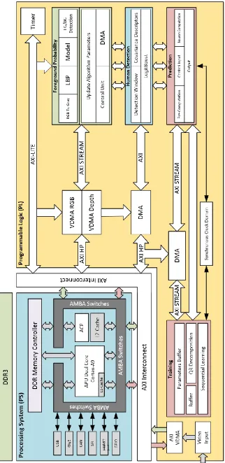
The proposed framework (Figure 1.4) was developed for complex human action
recognition or the Recognition of Actions “In the Wild” [22]. The parameters that
make recognition difficult are the following:
• Unknown camera motion
• Unknown camera viewpoint
• Lighting and shadow
• Undefined number of participants
For simple action recognition, the actions and motions of interest occur in a
con-strained environment, without the abovementioned variations. For better accuracy,
depth information is also included; however, the framework is capable of working
with both 2D and 3D streams. Since the camera viewpoint and camera motion
af-fect the results of point-of-interest detection, two stages of preprocessing are included
The Harris Corners 3D [22] [23] [24] and Hessian Corners 3D [25] [26] operators
are used as point-of-interest detection functions, and for later representation, the Bag
of Visual Words (BOW) approach is used as a feature descriptor. Finally, in the last
stage, an efficient machine learning algorithm that can recognizes the type of action
is required. The online sequential extreme learning machine (OS-ELM) [27] [28]
approach is a modified version of the ELM [29] [30] [31] [32] [33] approach that works
with chunks of data instead of passing whole frames of data. The advantages of this
method are, reduction resource utilization which is also more efficient for real-time
application. The Xilinx Zynq 7000 SoC-FPGA [34] is considered as the platform
for the implementation of the proposed framework. As represented in figure 1.5, all
modules are synthesized and implemented in the FPGA in order to accelerate their
operation.
The four major challenges hindering the embedded realization of the proposed
framework are as follows:
• The need for sufficient storage space to maintain and update the model.
• The use of appropriate bandwidth and access time to update the framework
parameters.
• Concurrent processing of and access to the modules aligned with the input
stream.
• An efficient interface for connecting to the camera that satisfies the bandwidth
requirement.
1.7
Organization of the Thesis
The remainder of this dissertation is organized as follows. Chapter 2 presents a brief
machine visionThe proposed approach for hardware acceleration for foreground and
background identification (foreground probability) and the communication interface
used to capture the stream and pass it to the memory block are discussed in chapter
3. The second stage of preprocessing, for identifying humans in the data stream and
the appropriate circuit for speeding up operation, is discussed in chapter 4. Chapter 5
discusses point-of-interest detection, the feature descriptor modules, and the results of
support vector machine (SVM)-based action recognition. Finally, the approach for the
implementation of the OS-ELM approach in hardware, the operation of the prediction
and training blocks and how these two blocks can be synced, and a comparison with
the resource utilization and performance of the SVM method are discussed in chapter
6, followed by the presentation of conclusions and the suggestion of topics for future
References
[1] “Digilent Nexys Video Artix-7 FPGA: Trainer Board for Multimedia
Appli-cations,” https://www.xilinx.com/products/boards-and-kits/1-cfdwic.html,
ac-cessed: 2018-04-18.
[2] “Integration of vision in embedded systems,”
https://www.vision-
systems.com/articles/print/volume-22/issue-1/features/integration-of-vision-in-embedded-systems.html, accessed: 2018-04-18.
[3] B. Senouci, I. Charfi, B. Heyrman, J. Dubois, and J. Miteran, “Fast prototyping
of a soc-based smart-camera: a real-time fall detection case study,” Journal of Real-Time Image Processing, vol. 12, no. 4, pp. 649–662, 2016.
[4] P.-J. Lapray, B. Heyrman, and D. Ginhac, “Hdr-artist: an adaptive real-time
smart camera for high dynamic range imaging,” Journal of Real-Time Image Processing, vol. 12, no. 4, pp. 747–762, 2016.
[5] “ITRS 2.0 PUBLICATION,” http://www.itrs2.net/itrs-reports.html, accessed:
2018-03-16.
[6] C. Mead and L. Conway, Introduction to VLSI systems. Addison-Wesley Read-ing, MA, 1980, vol. 1080.
[7] “Introduction of System-on-Chip,”
http://en.wikipedia.org/wiki/System-on-a-chip., accessed: 2018-03-16.
[8] “BOOST,” http://www.boost.org/., accessed: 2018-03-16.
[9] “OpenCL: the open standard for parallel programming of heterogeneous
sys-tems,” https://www.khronos.org/opencl/., accessed: 2018-03-16.
[11] “Digital Signal Processor,” https://en.wikipedia.org/wiki/Digital signal processor.,
accessed: 2018-03-16.
[12] “Digital Signal Processor (DSP),” http://www.ti.com/processors/dsp/overview.html.,
accessed: 2018-03-16.
[13] “Graphics Processing Unit (GPU),” https://en.wikipedia.org/wiki/Graphics processing unit.,
accessed: 2018-03-16.
[14] “Graphics Processing Unit (GPU),” http://www.nvidia.ca/object/gpu.html.,
ac-cessed: 2018-03-16.
[15] N. Einspruch, Application specific integrated circuit (ASIC) technology. Aca-demic Press, 2012, vol. 23.
[16] S. D. Brown, R. J. Francis, J. Rose, and Z. G. Vranesic,Field-programmable gate arrays. Springer Science & Business Media, 2012, vol. 180.
[17] “Intel SoCs,” https://www.altera.com/products/soc/overview.html, accessed:
2018-03-16.
[18] “Intel SoC FPGA Family,”
https://ca.mouser.com/new/altera/altera-socFPGA/, accessed: 2018-03-16.
[19] “ASIC, ASSP, SoC, FPGA What’s the Difference?”
https://www.eetimes.com/author.asp?section id=216&doc id=1322856,
ac-cessed: 2018-03-16.
[20] “Microsemi System on Chip FPGA,”
https://www.microsemi.com/products/fpga-soc/soc-fpgas, accessed: 2018-03-16.
[21] “SoCs, MPSoCs and RFSoCs,”
[22] S. Hadfield, K. Lebeda, and R. Bowden, “Hollywood 3d: What are the best 3d
features for action recognition?” International Journal of Computer Vision, vol. 121, no. 1, pp. 95–110, 2017.
[23] I. Laptev and T. Lindeberg, “Space-time interest points,” inIN ICCV, 2003, pp. 432–439.
[24] S. Hadfield and R. Bowden, “Hollywood 3d: Recognizing actions in 3d
natu-ral scenes,” in Computer Vision and Pattern Recognition (CVPR), 2013 IEEE Conference on. IEEE, 2013, pp. 3398–3405.
[25] G. Willems, T. Tuytelaars, and L. Van Gool, “An efficient dense and
scale-invariant spatio-temporal interest point detector,” in Computer Vision–ECCV 2008. Springer, 2008, pp. 650–663.
[26] P. R. Beaudet, “Rotationally invariant image operators.” in International Joint Conference on Pattern Recognition, 1978, pp. 579–583.
[27] H. T. Huynh and Y. Won, “Regularized online sequential learning algorithm
for single-hidden layer feedforward neural networks,” Pattern Recognition Letters, vol. 32, no. 14, pp. 1930 – 1935, 2011. [Online]. Available: http://www.sciencedirect.com/science/article/pii/S0167865511002297
[28] N.-Y. Liang, G.-B. Huang, P. Saratchandran, and N. Sundararajan, “A fast and
accurate online sequential learning algorithm for feedforward networks,” IEEE Transactions on Neural Networks, vol. 17, no. 6, pp. 1411–1423, 2006, cited By 736.
[29] G. Huang, G.-B. Huang, S. Song, and K. You, “Trends in extreme learning
machines: A review,” Neural Networks, vol. 61, pp. 32–48, 2015.
[30] J. Cao, Z. Lin, G.-B. Huang, and N. Liu, “Voting based extreme learning
[31] J. Tang, C. Deng, and G.-B. Huang, “Extreme learning machine for multilayer
perceptron,”IEEE transactions on neural networks and learning systems, vol. 27, no. 4, pp. 809–821, 2016.
[32] X.-Z. Wang, R. Wang, and C. Xu, “Discovering the relationship between
gen-eralization and uncertainty by incorporating complexity of classification,” IEEE transactions on cybernetics, vol. 48, no. 2, pp. 703–715, 2018.
[33] Z. Huang, Y. Yu, J. Gu, and H. Liu, “An efficient method for traffic sign
recog-nition based on extreme learning machine,” IEEE transactions on cybernetics, vol. 47, no. 4, pp. 920–933, 2017.
[34] “Xilinx Zynq 7000 SoC-FPGA,”
Chapter 2
Background
2.1
System-on-a-Chip (SoC)
2.1.1
Evolution
A system-on-a-chip (SoC) is a fabricated integrated circuit (IC) that consists of several
preverified blocks called intellectual properties (IPs). These IP cores could be DSP
blocks; memory blocks, such as DMA or VDMA; interface blocks, such as USB, SPI
or I2C; embedded processor cores; or other digital or analog blocks. The first SoC
was developed for the Microma watch in 1974; it was developed on a single Intel 5810
complementary metal-oxide-semiconductor (CMOS) chip to function as a driver for a
liquid crystal display (LCD) to control the timing function [1]. With the development
of technology for transistor manufacturing, the number of transistors that can be
fabricated on a single chip has increased, allowing more components and blocks to be
fabricated in a single IC. Figure 2.1 presents the general SoC architecture, and Figure
2.2 presents the modern SoC on which we developed and synthesized our framework.
Recently developed SoCs provide many IPs, such as a central processing unit
(CPU) as the key block, a memory controller, memory storage blocks, and additional
processing units that can act as co-processors or accelerators, such as application
processing units (APUs), real-time processing units (RPUs) and graphics processing
units (GPUs). Cores such as the ARM Cortex-A53 [4] are commonly used as APUs,
and ARM Cortex-R5 [5] and ARM Mali-400 MP2 [6] cores can serve as RPUs and
GPUs, respectively . A SoC also has a system bus for communication among the
Figure 2.1– General SoC architecture [2].
the AXI [7] buses developed based on the ARM AMBA [8] [9] protocol are some of
the best known. Depending on the type of application, a SoC may also offer some
general-purpose input/output (GPIO) or high-speed connectivity, such as through
SATA3.1, PCI Express, SATA, PS-GTR interfaces, or general connectivity, such as
through GigE, CAN or UART interfaces. In addition to the abovementioned
com-ponents, recent SoCs often include reconfigurable logic blocks (SoC FPGAs). Such
a reconfigurable block allows designers to synthesize soft IP cores, as well, such as
Figure 2.2 – Zynq-7000 SoC [3].
customized logic coded by the user. This provides more flexibility for designers to
use the same SoC for different applications.
2.1.2
Design Trends
The recent trends in SoC design are generally focused on the following items:
• Multi-Core Processor SoCs: Integrating more cores can increase the
pro-cessing capabilities of a SoC while also providing a more acceptable level of
solu-tion for modern design, especially for applicasolu-tions that require complex
com-putations. In this approach, it is not required that all cores be the same.
Fabricating cores such as APUs, RPUs and GPUs in the same die is common.
• Power Efficiency: As the density increases, the power consumption also
in-creases. To cope with this problem, some solutions have been proposed in which
idle cycles are introduced for some blocks to save power. Another approach is
to manage the clock distribution; instead of using multiple clock sources, the
system could operate on a single clock source, and the operation of each block
could be controlled based on a different phase of the clock.
• Reconfigurable Blocks: As mentioned above, some recent SoC components
(SoC FPGAs) include reconfigurable blocks to provide better flexibility for
de-signers. SoC-FPGAs have recently become popular in image and video
process-ing applications since most recent applications of this type have been developed
for portable systems, making SoC-FPGAs an excellent option for implementing
these algorithms.
2.1.3
Embedded Vision on a SoC
The algorithms that have been developed for machine vision applications consist of
the components represented in the following pipeline; however, depending on the type
of application, many of these components may be included or excluded. Because of
the complexity of the algorithms, the processors are often optimized for the
compute-intensive portions of the software workload. However, this approach is not applicable
for embedded vision systems or portable systems. Moreover, power limitations restrict
the deployment of machine vision algorithms in embedded systems, especially when
the input stream is of full-HD resolution. These restrictions could be overcome by
combining embedded processors with specialized hardware accelerators.
Image Acquisition
Lens Correction
Image
Pre-Processing Segmentation
Object
Analysis Heuristics
Figure 2.3– Machine vision framework pipeline.
with ADI ADSP-BF60x [7] and TI DaVinci [11]. In these platforms, the high-level
analytics are executed and controlled by a processor, while the computations for the
machine vision algorithms are performed by accelerators. However, these platforms
were developed for basic vision algorithms, such as vision filters, and advanced vision
algorithms, which, as mentioned above, consist of multiple blocks of much higher
complexity and irregularity of execution, have been left behind. In traditional
ap-proaches, custom hardware (accelerator) implementations are used for preprocessing,
and the remaining computations are executed on the host processor. Some processors
that support instruction-level parallelism (ILP) can speed up operation; however, the
communication bandwidth between the custom hardware and the processor restricts
the level of optimization. In recent solutions, an accelerator is integrated into the
sys-tem as a co-processor; as a result, the accelerator can access streaming data from the
system memory and system I/O and consequently lower the system traffic. Among
the available platforms for the realization of the custom hardware approach,
SoC-FPGA-based solutions are highly popular due to their balance between performance
and power efficiency. Although ASICs provide better power consumption, 5x-12x [12]
less than FPGAs, FPGAs are very efficient for both prototyping and real deployment
due to their much lower design and development costs.
2.2
AXI Interface
AXI is the communication interface protocol developed based on the ARM AMBA
[8] [9] [7] protocol for microcontrollers in 1996. The first version of AXI, AMBA 3.0,
known as AXI4. AXI4 is the main bus interface protocol for Xilinx Zynq SoC-FPGAs.
The AXI4 protocol includes three types of interfaces:
• AXI4: Developed for high-performance memory-mapped communication.
• AXI4-Lite: Developed for simple, low-throughput memory-mapped
commu-nication.
• AXI4-Stream: Developed for high-speed streaming data.
An AXI interface operates in both master and slave modes, represented by IP cores
that exchange information with each other. Master and slave IPs can be connected
using a structure called an interconnect block. The AXI Interconnect IP includes
AXI-compliant master and slave interfaces and can be used to establish communications
between one or more AXI masters and slaves. AXI4 and AXI4-Lite interfaces consist
of the following five different channels:
• Read Address Channel
• Write Address Channel
• Read Data Channel
• Write Data Channel
• Write Response Channel
Transactions can pass in both directions between the master and slave
simultane-ously and can operate at different transfer sizes. An AXI4-Lite interface can transfer
only 1 data transaction, whereas the burst operation in an AXI interface can transfer
up to 256 data transactions. Figure 2.4 shows how an AXI4 read transaction uses the
read address and read data channels.
As represented in the figures 2.4 and 2.5 , an AXI4 interface provides separate
Figure 2.4– AXI Architecture of Reads [13].
Figure 2.5– AXI Architecture of Writes [13].
separate channels is that doing so enables simultaneous, bidirectional data transfer.
An AXI4 transaction requires a single address and can burst up to 256 words of
data. AXI interfaces provide a variety of features that allow a system to achieve
high data throughput. These features include data upsizing and downsizing, multiple
outstanding addresses, and out-of-order transaction processing. Also, AXI4 allows the
use of a different clock for each AXI master-slave pair. Moreover, the AXI protocol
allows the insertion of register slices to aid in timing closure.
The difference between AXI4-Lite and AXI4 is the bursting operation, which is
Figure 2.6– AXI Interconnnect [13].
for the transmission of streaming data. The operation of AXI4-Stream is modeled
after that of the write data channel of AXI4. Unlike AXI4 interfaces, AXI4-Stream
interfaces can burst an unlimited amount of data. The additional features of
AXI-Stream include the splitting, merging, interleaving, upsizing, and downsizing of the
stream. Notably, the ability to reorder the transferred streams, which is available in
AXI4 and AXI4-Stream, is not applicable in AXI4-Stream.
2.2.1
Xilinx AXI Infrastructure IP
A Xilinx SoC-FPGA provides common IPs that are used in most designs. In this
section, we briefly discuss the main IPs that are used in many AXI-based systems.
The AXI Interconnect IP is utilized to connect one or more AXI master devices to
one or more slave devices (Figure 2.6).
The AXI Interconnect module consists of slave and master submodules and other
functional blocks, such as registers, a FIFO block, a clock converter, and upsizers and
downsizers, which manage the transactions between the master and slave. The slave
accepts write and read transactions at the request of the master, and the crossbar
module controls the traffic on all channels between the various devices connected to
Figure 2.7– N-to-1 AXI Interconnect (left), 1-to-N AXI Interconnect (right) [13].
depending on the architecture of the design. The modes in which an AXI interconnect
can operate are as follows:
• Pass-Through
• Conversion Only
• N-to-1 Interconnect
• 1-to-N Interconnect
• N-to-M Interconnect
In the pass-through mode, the transaction passes only between one master IP and
one slave IP; as a result, no conversion is required. The second mode, the
conversion-only mode, again involves communication between one master IP and one slave IP;
the following types of conversion can be employed by the interconnect:
• Data width conversion
• Clock rate conversion
Figure 2.8– N-to-M Interconnect [13].
• AXI-3 slave adaptation
• Pipelining, such as a register slice or data channel FIFO
The third and fourth modes are used when multiple master devices are required
to communicate with one slave (N to 1) or when a single master is required to
com-municate with multiple slaves (1 to N). A typical example of the third mode is the
operation of a memory controller, and a typical example of the fourth mode is when
a processor is required to communicate with multiple peripherals. The arbiter and
decoder/router are required to control the operation of N-to-1 and 1-to-N
commu-nication. The last mode is used when multiple IPs are required to communicate
with each other. In this mode, the arbiter and decoder work together to control the
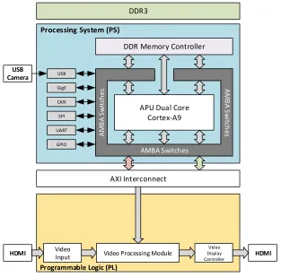
DDR Memory Controller
APU Dual Core Cortex-A9
USB
Processing System (PS)
DDR3 GigE CAN SPI UART GPIO Video Input AXI Interconnect
Video Processing Module
Video Display Controller AMBA Switches A M B A S w itc h
es AMB
A S w itc h es USB Camera HDMI HDMI
Programmable Logic (PL)
Figure 2.9– Direct streaming.
2.3
Streaming Architectures
There are two main approaches available for the implementation of machine vision
algorithms on embedded platforms. The first approach is “direct streaming”. The
input stream arrives directly from the communication link; the vision algorithm is
directly employed, and the result is passed to the output interface. This approach
offers the simplest and most efficient processing; however, it requires the design of
components that can process frames in real time (Figure 2.9). In the second approach,
which is called “frame-buffer streaming”, the input stream is first stored in a memory
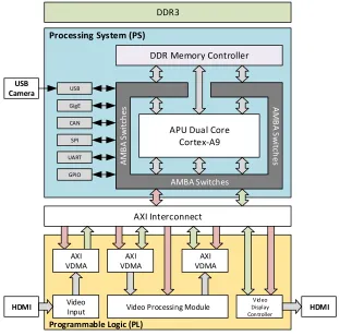
DDR Memory Controller
APU Dual Core Cortex-A9
USB
Processing System (PS)
Programmable Logic (PL)
DDR3 GigE CAN SPI UART GPIO AXI VDMA Video Input AXI VDMA AXI VDMA
Video Processing Module
Video Display Controller AMBA Switches A M B A S w itc h
es AMB
A S w itc h es USB Camera HDMI HDMI AXI Interconnect
Figure 2.10 – Frame-buffer streaming.
processing it, stores it again in another block of memory (VDMA). The display of
the results is controlled by another component that has access to this second block
of memory. Therefore, there is no additional overhead for the video processing block.
This approach offers more decoupling between the video rate and the processing
speed of the video components. However, it requires a sufficient memory bandwidth
2.4
System Profiling
Recently, the utilization of embedded SoC systems has grown rapidly as processing
capabilities have increased. In addition, the market is demanding simpler and more
efficient designs. In an efficient design, the final product should have the optimal
partitioning of hardware and software. For this reason, tools such as profilers plays
an important role in determining which function or component is the bottleneck in a
system. Profilers assist designers in creating a proper balance between hardware and
software in a system.
Since most of a SoC consists of embedded processors and accelerators, such as
FPGAs and GPUs, finding the bottleneck function in the processor framework that
slows the operation is achieved by executing the same function with an accelerator,
and how the operation is optimized is essential. There are three main approaches
available for system profiling: software-based profiling (SBP), hardware-based
profil-ing (HBP), and FPGA-based profilprofil-ing.
In SBP, function performance is evaluated using tools coded in the programming
language of the system. The profiler keeps track of all processes running in the
processor and helps the designer to identify the functions that make the operation
slow. Profilers in this category include IDE tools such as Visual Studio.
Tools of the second type (HBP) use the counters integrated in the chips. Most
common processors, such as Sun UltraSPARC processors, Intel Pentium processors,
and Advanced Micro Devices (AMD) processors use dedicated counters to measure
the execution of target functions. The advantages of this approach are that it does
not interfere with the operation of the processor and data are collected during run
time.
In the last approach, reconfigurable logic is used to measure performance. This
approach can generally be used to measure the performance of soft core processors,
core processors, such as ARM processors, which are fabricated in SoC-FPGAs. The
profiling components could be counters or timers that are synced with the processor
References
[1] “Computer History Museum,”
http://www.computerhistory.org/siliconengine/digital-watch-is-first-system-on-chip-integrated-circuit/., accessed: 2018-03-16.
[2] “System On a Chip,” https://en.wikipedia.org/wiki/System on a chip,
ac-cessed: 2018-03-16.
[3] “Zynq-7000 Programmable SoC Product Advantages,”
https://www.xilinx.com/products/silicon-devices/soc/zynq-7000.html,
ac-cessed: 2018-03-16.
[4] “ARM Cortex-A53,”
https://developer.arm.com/products/processors/cortex-a/cortex-a53, accessed: 2018-03-16.
[5] “ARM Cortex-R5,”
https://developer.arm.com/products/processors/cortex-r/cortex-r5, accessed: 2018-03-16.
[6] “ARM Mali-400 MP2,”
https://www.arm.com/products/graphics-and-multimedia/mali-gpu, accessed: 2018-03-16.
[7] “AMBA AXI4 Interface Protocol,”
https://www.xilinx.com/products/intellectual-property/axi.html, accessed: 2018-03-16.
[8] “AMBA Introduction,”
https://developer.arm.com/products/architecture/amba-protocol, accessed: 2018-03-16.
[9] “AMBA SPECIFICATIONS,”
https://www.arm.com/products/system-ip/amba-specifications, accessed: 2018-03-16.
[10] “Xilinx MicroBlaze,”
[11] “TIs processors leading the way inembedded analytics,”
http://www.ti.com.cn/cn/lit/wp/spry280/spry280.pdf, accessed:
2018-03-16.
[12] I. Kuon and J. Rose, “Measuring the gap between fpgas and asics,”IEEE Trans-actions on computer-aided design of integrated circuits and systems, vol. 26, no. 2, pp. 203–215, 2007.
[13] “AMBA AXI4 Interface Protocol,”
https://www.xilinx.com/products/intellectual-property/axi.html, accessed: 2018-03-16.
[14] “Nios II Processor,” https://www.altera.com/products/processors/overview.html,
Chapter 3
System-On-a-Chip (SoC)-Based Hardware
Acceleration For Foreground And
Background Identification
3.1
Introduction
Embedded vision has experienced significant technological breakthroughs in recent
years by virtue of the development of enabling technologies for the implementation
of different and complex image and video processing algorithms with improved
per-formance, higher efficiency, and reduced cost. Among these technologies, hardware
acceleration has been critical to the development of such systems because it allows
certain functions to be performed more efficiently than is possible in software running
on a more general-purpose processor.
For the implementation of a vision algorithm, two main approaches are
avail-able. First, microprocessors (µPs) and digital signal processors (DSPs) offer
all-software solutions that can meet the requirements of most applications, along with
a complete set of development tools. Second, hardware acceleration, in the form of
field-programmable gate arrays (FPGAs) or graphics processing units (GPUs), can
perform specific tasks that are not suitable for µPs or DSPs. However, GPUs tend
to have high power consumption, making them challenging to deploy in embedded
environments.
Recent advances in silicon technology have brought to the market FPGA and
de-manding algorithms. In the new generation of system-on-a-chip field-programmable
gate arrays (SoC-FPGAs), both a microprocessor and an FPGA are included on a
single chip. Such a device consumes less power and can be incorporated into smaller
systems, offering an attractive platform for embedded applications and making
SoC-FPGA technology well suited for embedded systems from the perspectives of
perfor-mance and cost.
With the recent increase in processing capabilities, machine vision algorithms are
being increasingly implemented in embedded systems. Embedded vision, defined as
the implementation and execution of visual analysis and computer vision algorithms
using embedded systems [1], is an active topic in the field of embedded platforms
that covers a variety of applications, such as autonomous vehicles, smart cameras
[2] [3], industrial vision cameras, sensor networks and security systems (surveillance
systems). The surveillance market alone is estimated to have more than tripled in
the past decade, from $11.5 billion in 2008 to $37.5 billion in 2015 [4].
Most embedded vision applications feature common top-level requirements. First,
a sequence is sampled at a number of spatio-temporal locations, and then, local feature
descriptors are extracted. As the next step, the local features are encoded into a
holistic descriptor, and finally, a discriminative classifier is used to identify likely
categories. The main challenge in embedded vision systems is the tradeoff between
power consumption and performance, where the power consumption becomes more
important when the device is battery powered.
Some vision algorithms have been developed for specific streams and
environ-ments. Thus, the structure of such an algorithm requires constant updating of the
parameters, and the quality of the output result is determined by the specific input
to the algorithm. The type of application that is most appropriate for this method is
vision filtering. Another type of algorithm that is currently of interest to researchers
is adaptive vision algorithms, which are defined in terms of a model that is updated
with different types of inputs and in different types of environments, but they require
considerable bandwidth and high-performance hardware. Most adaptive vision
al-gorithms are based on machine learning principles, such as support vector machines
(SVMs), extreme learning machines (ELMs) [5] [6] [7] and mixtures of Gaussians
(MoGs), which require training steps; this could be another task for development.
The emergence of commercial full-HD cameras and depth sensors and the market
desire for high-resolution processing have given rise to a need for a platform that
can capably perform complex computations requiring many billions of operations per
second (GOPS). As a result, high-resolution processing requires considerable power;
however, for an embedded platform powered by a battery, the power consumption
must be less than 1 W, which could pose a challenge for high-quality vision
process-ing applications. The main challenges facprocess-ing the implementation of adaptive vision
algorithms on hardware, particularly when the input stream is of HD resolution, are
as follows:
• The use of a storage space that can maintain and update the model;
• The use of an appropriate bandwidth and access time to update the model
parameters;
• Concurrent processing and access to the model aligned with the input stream;
and
• An efficient interface for connecting to the camera that satisfies the bandwidth
requirement.
As mentioned above, traditional implementations are mainly restricted to
filter-ing operations such as illumination or color enhancement or edge extraction. In
most algorithms, these procedures require information only on the current frame
and consequently have fairly low data storage and bandwidth requirements.
![Figure 2.1 – General SoC architecture [2].](https://thumb-us.123doks.com/thumbv2/123dok_us/1361178.1168945/41.612.164.484.87.459/figure-general-soc-architecture.webp)
![Figure 2.2 – Zynq-7000 SoC [3].](https://thumb-us.123doks.com/thumbv2/123dok_us/1361178.1168945/42.612.169.486.80.449/figure-zynq-soc.webp)

![Figure 2.4 – AXI Architecture of Reads [13].](https://thumb-us.123doks.com/thumbv2/123dok_us/1361178.1168945/46.612.163.488.67.442/figure-axi-architecture-of-reads.webp)
![Figure 2.8 – N-to-M Interconnect [13].](https://thumb-us.123doks.com/thumbv2/123dok_us/1361178.1168945/49.612.109.543.72.337/figure-n-to-m-interconnect.webp)