ABSTRACT
QU, ZHI. Reducing MCU Utilization and Output Voltage Variance for Software Controlled SMPS. (Under the direction of Dr. Alexander Dean).
Providing high quality power conversion with high efficiency and low cost has been
studied by a lot of people. Although switch mode power supply (SMPS) has been popular
with high end systems, it is not so widely used by low end systems because of its
requirements for additional hardware and computational resources.
This thesis builds a software SMPS controller for synchronous buck converter to
regulate the output voltage. Comparisons between feedback and feed forward control
algorithm as well as time triggered and event triggered mechanism are drawn in terms of
© Copyright 2015 Zhi Qu
Reducing MCU Utilization and Output Voltage Variance for Software Controlled SMPS
by Zhi Qu
A thesis submitted to the Graduate Faculty of North Carolina State University
in partial fulfillment of the requirements for the degree of
Master of Science
Electrical Engineering
Raleigh, North Carolina
2015
APPROVED BY:
_______________________________ ______________________________
Dr. Alexander Dean Dr. Subhashish Bhattacharya
Committee Chair
DEDICATION
Dedicated to
My parents
Lianfa Qu and Liping Jiang
And my lovely girlfriend
BIOGRAPHY
Zhi Qu was born on April 18, 1990 in Dalian, China. He developed his interest in
mechatronics since his childhood when he built and tested controlled and uncontrolled
robotic cars and flights. After graduating from Dalian Yuming High School, he went to
Harbin Institute of Technology where he got a Bachelor of Science degree with a
concentration in Control Science and Technology. During his senior year in college, Zhi
worked with Dr Maorui Zhang and Yanliang Dong to build and test a hydraulic flight
simulator when he published two papers in control theory. Then he joint North Carolina State
University as a graduate student in the Electrical and Computer Engineering Department.
With some more courses in control theory, Zhi decided to focus in embedded system which
would give him a broader view of the system. Under the guidance of Dr Alexander Dean, he
implemented control software for buck converter in different embedded environments and
ACKNOWLEDGMENTS
I would like to express my sincere gratitude to Dr Alexander Dean who has been very
understanding and supportive. His guidance and encouragement have been helping me in
TABLE OF CONTENTS
LIST OF TABLES ... iii
LIST OF FIGURES ... iii
CHAPTER 1INTRODUCTION ... 1
1.1 Motivation ... 1
1.2 Preview of the Work ... 1
1.3 Outline of the Thesis ... 2
CHAPTER 2BACKGROUND ... 2
2.1 Synchronous buck converter ... 2
2.2 Buck Converter’s Response to Load Transient ... 2
2.3 Controller Design ... 2
2.3.1 PI Controller... 2
2.3.2 Feed Forward Controller ... 2
2.4 Real Time Management ... 2
CHAPTER 3SYSTEM DESIGN ... 2
3.1 Synchronous Buck Converter Operating Principle ... 2
3.2 Feedback Control loop ... 4
3.2.2 Implementing PI controller ... 6
3.3 Feed Forward Control ... 2
3.3.1 Output Impedance ... 2
3.3.2 Feed Forward against Feedback... 3
3.3.3 Frequency Domain Forward Control Analysis ... 2
3.3.4 Implementing Feed Forward Controller ... 2
3.4 Event triggered control ... 4
3.4.1 Introduction to event triggered control ... 5
3.4.2 Control algorithm execution time ... 2
3.4.3 Sequence Diagram ... 2
3.4.4 Sampling Position ... 2
3.4.5 Event triggered source code ... 4
3.5 DMA triggered AD conversion ... 6
4.3 Feedback Control Result ... 3
4.4 Feed Forward Control Result ... 7
4.5 Event triggered Control Result ... 2
4.6 DMA triggered AD conversion ... 10
4.7 Task blocking impact ... 11
4.8 Analysis ... 13
CHAPTER 5CONCLUSION AND FUTURE WORK ... 2
5.1 Conclusion ... 2
5.2 Future Work ... 2
REFERENCES ... 2
APPENDIX ... 2
APPENDIX ... 3
LIST OF TABLES
Table 1 Load Module Operation Voltage ... 2
Table 2 Buck converter parameters ... 2
LIST OF FIGURES
Figure 2-1 Buck Converter Circuit ... 2
Figure 2-2 Buck Converter transient response to load current increase [6] ... 3
Figure 2-3 Control Diagram for Buck Converter with Feed Forward Control ... 2
Figure 3-1 Photo for Synchronous Buck Converter ... 2
Figure 3-2 Schematic for Synchronous Buck Converter ... 2
Figure 3-3 Transient time for PWM signal ... 3
Figure 3-4 PWM signal with dead time ... 4
Figure 3-5 Loading transient of Buck Converter Regulated by PI controller ... 5
Figure 3-6 PWM Signal Regulating Buck Converter Output Voltage ... 6
Figure 3-7 Sequence Diagram of Control Loop ... 7
Figure 3-8 Fixed Point Math Flow Chart ... 2
Figure 3-9 Enhanced Fixed Point Math Sequence Diagram ... 3
Figure 3-10 Execution time of ADC ISR ... 4
Figure 3-11 Feedback control diagram with current load transient ... 3
Figure 3-12 Load current to output voltage diagram ... 2
Figure 3-13 Bode Plot from change in load current to change in output voltage ... 2
Figure 3-14 Load Current to Output Voltage With Feed Forward Control Loop Diagram .. 3
Figure 3-15 PWM signal with proportional feed forward control ... 4
Figure 3-16 Output voltage with proportional feed forward control ... 5
Figure 3-18 Output voltage with differential feed forward control ... 7
Figure 3-19 Output voltage with differential feed forward control in large time scale ... 8
Figure 3-20 Output voltage with PD feed forward control ... 9
Figure 3-21 Sequence Diagram for feed forward controller ... 2
Figure 3-22 Event triggered Control Diagram ... 2
Figure 3-23 Event triggered feed forward control diagram ... 4
Figure 3-24 Typical loading transient for buck converter ... 2
Figure 3-25 Loading transient for buck converter with feed forward and resetting ... 3
Figure 3-26 DMA Triggered Sequence Diagram ... 8
Figure 4-1 Refined PLECS model for buck converter... 2
Figure 4-2 Constant Current Source ... 2
Figure 4-3 Load current transient ... 2
Figure 4-4 PI controller PLECS model ... 3
Figure 4-5 Simulated output voltage when load transient occurs ... 4
Figure 4-6 Output voltage of buck converter when load transient occurs ... 5
Figure 4-7 Computational resources consumed by updating duty cycle ... 6
Figure 4-12 Simulated output voltage when load transient occurs with feed forward control
delayed ... 10
Figure 4-13 MCU utilization by updating duty cycle in each period with feed forward control ... 11
Figure 4-14 PLECS model for event triggered PI control ... 2
Figure 4-15 Simulated output voltage when load transient occurs with event triggered control ... 2
Figure 4-16 Output voltage when load transient occurs with event triggered control... 3
Figure 4-17 MCU utilization with event triggered control ... 4
Figure 4-18 Number of ISR triggered when current changes ... 5
Figure 4-19 PLECS model for event triggered PI control with feed forward control ... 6
Figure 4-20 Simulated output voltage when load transient occurs with event triggered and feed forward control ... 7
Figure 4-21 Output voltage when load transient occurs with event triggered feed forward control ... 8
Figure 4-22 MCU utilization with event triggered feed forward control ... 9
Figure 4-23 MCU utilization with event triggered feed forward control ... 10
Figure 4-24 Outpot voltage and MCU utilization with DMA ... 11
Figure 4-25 Blocking time VS Maximum Voltage Drop ... 13
CHAPTER 1
INTRODUCTION
1.1 Motivation
Converting power efficiently has long been interested in and studied. For embedded systems,
several voltage rails are required to drive different components which require conversion of
power. Compared to other DC-DC converters, linear-regulator with lower efficiency number
has been the choice for cost sensitive systems as it doesn’t require additional dedicated micro
controller unit (MCU). In AVS project, we want replace linear-regulator with high efficiency
buck converter without using additional MCU. This requires utilizing existing MCU in a
system to run the application and regulating output voltage of buck converter at the same
time.
For power supply of a system, output voltage variation caused by load current and input
voltage change is desired to be small to eliminate malfunctioning. In our application, this is
challenged by the fact that detection and regulation of output voltage can be delayed by other
applications. In this thesis, I focus on how to regulate output voltage when load current
developed software which monitors output voltage and update duty cycle of PWM signal to
drive the buck converter.
In addition to the conventional control method of closed loop PI controller, an additional
ADC channel is used to implement the feed forward control which would reduce the
maximum output voltage drop when load current changes. Later, we used event triggered
control mechanism to replace previously used time triggered control mechanism to reduce
the MCU utilization. Finally, DMA is used to configure and trigger AD conversion to further
reduce MCU utilization.
1.3 Outline of the Thesis
The rest of this thesis is organized as follows: Chapter 2 discusses the synchronous buck
converter we use, the closed loop PI controller, feed forward controller and the real time
management technique used in our system. Chapter 3 analyzes these techniques and gives
detailed description about how these techniques are implemented with time triggered and
event triggered mechanism. Chapter 4 shows how these techniques work in simulation and in
our circuit and then discusses how the hardware we need to build the system, the maximum
output voltage variance and the MCU utilization interacts with each other. In Chapter 5, the
CHAPTER 2
BACKGROUND
In this chapter, we will look into back ground information for our system. In this system, we
use synchronous buck converter to achieve high efficiency. Several control techniques and
scheduling method are used to ensure voltage regulation and fast response at load transient.
2.1 Synchronous buck converter
“The buck converter has a capacitor and an inductor along with two complementary
switches; when one switch is closed, the other is opened and vice versa. The switches are
alternately opened and closed at the rate of the PWM switching frequency. The output that
results is a regulated voltage of smaller magnitude than the source voltage”. [1]
In conventional buck converter, a diode is used as rectifier whose large forward voltage drop
introduces a lot of power losses during freewheeling time. The synchronous buck converter
replaces freewheeling diode by MOSFET switch and utilize the low forward voltage drop
across the intrinsic diode to conduct freewheeling current. The ideal synchronous buck
Figure 2-1 Buck Converter Circuit
Digital control methods are widely used in controlling the buck converter. [2][3] Voltage mode control [4] and current mode control [5] are the two main control structure that has been
used. In voltage mode control, the transistor can be driven by PWM signal, depending on
whether they are PMOS or NMOS, the gate drive signal of the two transistor are
complementary or the same. If we define the ratio of on time during one period for FET1 as
D, the ideal relationship between in input and output voltage is as following. This
relationship is valid when considering all components to be ideal.
𝑉𝑜𝑢𝑡 = 𝑉𝑖𝑛𝐷
2.2 Buck Converter’s Response to Load Transient
Embedded systems typically include a set of peripherals besides the microcontroller to
achieve its functionality. The requirements of application or energy saving make the
supply is thus increasing (a loading transient) or decreasing (an unloading transient) through
time. The magnitude of current change can reach tens of mA (SD memory card access, high
brightness LEDs, Bluetooth radio) or hundreds of mA (WiFi module).
For ideal buck converter model, the output voltage is exclusively dependent on input voltage
and duty cycle. However, due to the series resistance of components and finite inductance
and capacitance, the output voltage will have both transient and steady state voltage changes
when load current change occurs.
Figure 2-2 Buck Converter transient response to load current increase [6]
Figure 2-2 shows several possible transient response in output voltage when load transient
2.3 Controller Design
Since components in real world are not all ideal. The series resistance as well as voltage drop
across rectifiers would cause the actual output voltage differ from calculation based on ideal
relationship. Typically a closed loop control system is used to make sure the output voltage is
following the set point.
2.3.1 PI Controller
“As known to all, the PI control is the typical method in electrical engineering, which is the
linear controller as well.”[7] In buck converter design, a PI controller is often used to regulate the output voltage. A PI controller calculates the error between the set point and actual output
voltage and adjust the duty cycle of PWM signal. The P part depends on the present error and
the I part depends on the integration of past errors. The transfer function of PI controller is
shown below.
𝐶(𝑠) = 𝐾𝑝+
𝐾𝑖 𝑠
2.3.2 Feed Forward Controller
Feedback control system is a control method with error. The system has to react according to
the error that has already occurred. This characteristic introduces a time delay that is hard to
compensate. The well-known derivative controller can be used as predictor of future error
and thus reduce the delay. However, for high bandwidth system, derivative controller is
Feed forward control, on the other hand, is a control method without error. Ideally, we can
compensate for the error before it occurs. In our application, the majority of voltage change
is caused by load current change. By measuring output current and adjusting duty cycle
accordingly, it’s possible to eliminate voltage variation in theory. In practice, due to the delay
caused by digital controller and the inertia of the system, there will still be some output
voltage variation but it will be much reduced. Output current [8] and capacitor current [9] are used as the feed forward sensing variable. However, since the output current is larger in
amplitude and thus easier to measure with smaller error, we adopted this in our system. A
diagram showing the control architecture of the system is shown in figure 2-3. The form of
feed forward controller 𝐺𝑐𝑓𝑓 can be designed according to the transfer function of 𝐺𝑣𝑑 and
2.4 Real Time Management
Having different dependent or independent tasks running at the same time with one or limited
amount of MCU is a common need for embedded system. Dividing the MCU’s time for
different application becomes an important job for finishing the work required correctly and
in time. “The decision determines how responsive the system is, which then affects how it
determines how fast a processor we must use, how much time we have for running intensive
control algorithms, how much energy we can save, and many other factors ” [10].
A scheduler (or kernel) is responsible for dividing processor’s time and distributing them to
different program. Whenever a program requests to be executed (this is called released), the
scheduler would put it in the list and figure out what its priority is (used for selecting which
program to run first). A non-preemptive scheduler will always finish the program it’s
currently running even if a higher priority task is released. A preemptive scheduler, on the
CHAPTER 3
SYSTEM DESIGN
In this chapter, detailed information about why and how the techniques we used in this
system is given. Additionally, the dead time between two gate drive signals and controller
design are described and analyzed.
3.1 Synchronous Buck Converter Operating Principle
A synchronous buck converter is built to test the control algorithm proposed. The photo of
Figure 3-2 Schematic for Synchronous Buck Converter
In this design, the high side MOSFET and the low side MOSFET are different channel. For
ideal components, we can simply drive them with the same gate drive signal. However, the
real gate drive signal has transients as shown in figure 3-3. In our case, a 50kHz PWM signal
is used as gate drive signal and it has 40 ns of transient time. At transient time, the two
MOSFETs may both work in their linear region instead of saturation or cutoff mode for a
Figure 3-3 Transient time for PWM signal
An additional PWM signal is used to solve this problem. The two PWM signals are central
aligned and a short dead time is added to the second PWM signal. Figure 3-4 shows the
t
t t t
PWM signal 1
PWM signal 2
Figure 3-4 PWM signal with dead time
If we have ∆𝑡 equal to or larger than the transient time of our gate drive signal, the two
MOSFETs won’t work at their linear region simultaneously and thus eliminate the existence
of short circuit time.
3.2 Feedback Control loop
3.2.1 PI Controller for Buck Converter
The modeling of buck converter is very well studied and the small signal duty cycle to output
voltage transfer function for ideal buck converter is shown below.
𝐺𝑣𝑑 =𝑉𝑖𝑛 𝐷
1
A PI controller is first used to regulate this system and the closed loop output voltage is
simulated in PLECS. The output voltage transient (Figure 3-5) and corresponding PWM
control signal (Figure 3-6) is shown.
Figure 3-6 PWM Signal Regulating Buck Converter Output Voltage
This simulation gives typical loading transient response of PI regulated buck converter. The
output voltage of buck converter is immediately affected when load transient occurs while
the duty cycle of PWM signal takes several periods to increase which would compensate for
the voltage drop.
3.2.2 Implementing PI controller
3.2.2.1 Sequence Diagram
Implementing PI controllers requires the system to work at a fixed frequency. Typically, a
higher operating frequency exhibits better performance with the same control method
indicates sampling and computing more frequently which requires more resources. Besides,
PI controller requires knowledge about the time the data is sampled. So we need a
synchronizing mechanism to ensure the sequential operations occur in order.
In considering of all these factors, we decided to make the system work at 50 kHz which is
the same as the operating frequency of the buck converter. This is a balanced choice among
buck converter efficiency, output voltage ripple, computational resource required and control
loop performance. The timing sequence of controlling the buck converter is shown in Figure
3-7.
3.2.2.2 PI Controller Discretization
In tradition continuous time control, PI controller refers to a controller of the form,
𝐺𝑐(𝑠) = 𝑘𝑝+
𝑘𝑖
𝑠
For discrete time system, integration is implemented by adding all previous error together
which gives the controller a form
𝐷(𝑧) = 𝑘𝑝𝑑+ 𝑘𝑖𝑑(1 + 𝑧−1+ 𝑧−2+ ⋯ )
In our implementation, the calculation is implemented in the form
𝑑(𝑛) = 𝑑(𝑛 − 1) + 𝑘1𝑒(𝑛) + 𝑘2𝑒(𝑛 − 1)
3.2.2.3 Fixed Point Math
Accuracy of the control loop is another factor of vital importance in the performance of
control loop. The first thought in achieving this is sampling and calculating with as many
digits as we can to keep high accuracy. However, considering the fact that MCUs we target
on don’t have floating point math unit, calculating for duty cycle with floating point numbers
is extremely slow (50us for FRDM-KL25Z) compared to the operating frequency of our
system (50 kHz). Besides, the accuracy of our ADC is also limited (16 bits) which puts a
limit on the accuracy we can get. In order to achieve fast calculation with appropriate
accuracy, we decided to implement control algorithm with fixed point math.
Typical fixed point math implementation includes 3 steps. First, we need to transform the
cycle with data in specific formation and convert the result back into regular formation.
Finally, we need to calculate for the PWM signal on time according to the period.
Data
transformation Calculation
ADC Reading Output voltage in 8-8 form
Pre-determined 8-8 form controller gain
PWM duty cycle in 16-16 form
Data transformation
PWM on time
Figure 3-8 Fixed Point Math Flow Chart
Figure 3-8 shows the process using 16 bits register to calculate with data and gain
represented in 8-8 format (8 bits integer and 8 bits decimal), get duty cycle in 32 bits 16-16
format (16 bits for integer and 16 bits for decimal) and finally get the on time for PWM
control.
By implementing fixed point math, the execution time for calculating next duty cycle for
PWM signal is much reduced to around 4 us for FRDM-KL25Z (Si’s paper). This enables us
to update duty cycle every period and makes it possible for the control loop to work at the
The original ADC reading has a different form of data. Each unit represents (3.3/65536)V
and we can use that to do the calculation directly. In addition, we can format our controller
gain so that after multiply-accumulation, the result equals to PWM on time. In this way, we
can eliminate two times of data transformation by re-formatting our controller gain and that
would reduce the time required for calculation tremendously.
In our program, we shifted the data to the left by 16 bits to get higher resolution. This is quite
important because the controller gain for buck converter working at 50 kHz is quite small
and it will become un-representable with too few digits of resolution.
Calculation
Modified controller gain
PWM on time shifted right
by 16 bits Shifting right by
16 bits
PWM on time ADC Reading
Figure 3-9 Enhanced Fixed Point Math Sequence Diagram
The modified controller gain can be determined with equation
𝑘1′ = 𝑇𝑠𝑘1∗𝑉𝑟𝑒𝑓
2𝑛 ∗ 216 = 216−𝑛𝑉𝑟𝑒𝑓𝑇𝑠𝑘1
𝑘2′= 𝑇𝑠𝑘2∗𝑉𝑟𝑒𝑓
2𝑛 ∗ 216= 216−𝑛𝑉𝑟𝑒𝑓𝑇𝑠𝑘2
𝑘1′---modified proportional controller gain
𝑘1---original proportional controller gain
𝑘2---original integral controller gain
𝑉𝑟𝑒𝑓---reference voltage for the microcontroller ADC module
𝑛---number of digits for the microcontroller ADC module
With the same hardware, we got the execution time for control loop further down to 1.28us
as shown in figure 3-10. A GPIO output is forced to be high when controller related
3.2.2.4 PI control loop source code
With all the problem solved above, the source code for PI controller is implemented with
additional code to keep the converter work in safe region and ensure there’s no overflow in
the calculation. reg=ADC0->R[0]; errorp=error; error=Vref-reg; d=dreg<<16; d=d+error*50+30*errorp; if(d>DutyCycleUpperBound) { TPM0->CONTROLS[4].CnV=470; }
else if(d< DutyCycleLowerBound) { TPM0->CONTROLS[4].CnV=20; } else { TPM0->CONTROLS[4].CnV=d>>16; TPM0->CONTROLS[3].CnV=TPM0->CONTROLS[4].CnV+8; } dreg=TPM0->CONTROLS[4].CnV;
Note that there’s one more step for registering and recovering from dreg. This acts the same
way as having no dreg and use TPM0->CONTROLS[4].CnV itself as a register. This
provides protection so even if something changes TPM0->CONTROLS[4].CnV after I
update it, I can still get the right duty cycle for next period. Also, it doesn’t take much time to
execute and provides an easier entry for more control algorithm implementation.
The other part that is important in this program is the timer interrupt. It will trigger the AD
conversion and we can modify the TPM interrupt in need of control architecture. In PI
control, this is quite simple and is introduced mainly to present a base case for comparison.
NVIC_ClearPendingIRQ(ADC0_IRQn); TPM0->SC|=TPM_SC_TOF_MASK; ADC0->SC2 =0;
ADC0->SC1[0] = 0x48;
3.3 Feed Forward Control
Feed forward is a control method that has no error in theory. It’s very responsive and can be
combined with feedback control to achieve very good control characteristic. In this section,
feed forward control is implemented for system with time triggered feedback control loop.
3.3.1 Output Impedance
In traditional control theory, we only consider single input single output system. Buck
converter, on the other hand, has multi inputs. The duty cycle, input voltage and output
current are all input to the system and influence the output of the system – output voltage.
The reason we can analyze a multi-input system with a theory dedicated to single input
system is because we consider one input to be our main concern and take all other inputs as
disturbance and compensate for them with closed loop. This method is widely used but it
may not provide the best performance for some system.
This is also known as output impedance.
3.3.2 Feed Forward against Feedback
As we discussed in previous section, the problem with feedback control is its respond to
change in load current is very slow. This is caused by the fact that it takes time for the control
loop to adjust duty cycle to compensate for load current change and for buck converter to
react to change in duty cycle (Figure 3-11).
vd
G
I out
Z
cfbG
d Vr + -+ +
Figure 3-11 Feedback control diagram with current load transient
Buck converter’s ability to change output voltage in respond to change in duty cycle is
determined by its structure. It’s dependent on price and technical requirements. Making a
buck converter that’s responsive to change in duty cycle and insensitive to change in load
The other way of increasing the responsiveness of the system is to increase the bandwidth of
the controller. However, the bandwidth of the feedback controller is limited by the
requirement of stability which is so important that people would typically trade some
bandwidth for stability margin.
One way to get exempt from the delay when compensating for load current change is by
creating a channel that directly goes from it to duty cycle change (Figure 2-3). In this case,
the delay between the time load current change and the time duty cycle reacts to it is reduced
in two ways.
The first reduction comes from the fact that the bandwidth of 𝑍𝑜𝑢𝑡 is also limited and is
probably designed to be as small as possible which is desirable for buck converter design.
Bypassing the output impedance eliminates the delay caused by it but the benefit is limited
because 𝑍𝑜𝑢𝑡 typically is not the main reason for delay.
The other source of reduction in responding time comes from the unlimited bandwidth of
feed forward controller 𝐺𝑐𝑓𝑓. As discussed before, the stability of system is limiting the
bandwidth of 𝐺𝑐𝑓𝑏 which is delaying the response of buck converter a lot. Feed forward
controller, on the other hand, doesn’t influence the stability of feedback loop and thus can
3.3.3 Frequency Domain Forward Control Analysis
Conventional control theory analyzes system characteristic in frequency domain. The type of
system we can analyze is limited to single input single output (SISO) linear time invariant
(LTI) system. In our case, two inputs (change in load current and change in reference
voltage) are considered.
However, we don’t actually need to consider the change in reference voltage because what
we are trying to do is to provide a fixed output voltage power source. Considering the change
in reference voltage ∆𝑟 as 0, we can reorganize the feedback control loop (Figure 3-12).
I out
Z
+ -vdG
G
cfbV
Figure 3-12 Load current to output voltage diagram
Figure 3-12 shows that the plant and feedback controller are on the ‘sensor part’ of a control
loop. This clearly explains that if we consider a particular buck converter, which means 𝑍𝑜𝑢𝑡
and 𝐺𝑣𝑑 are fixed, the effect of load current change is greatly dependent on feedback
controller whose bandwidth is limited by stability.
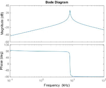
The closed loop transfer function from ∆I to ∆V is
∆𝑉 ∆𝐼 =
A bode of the transfer function from ∆I to ∆V (Figure 3-13) is shown to show that the effect
of change in current is not very well damped as it should be as we have limited closed loop
bandwidth.
I out
Z
+ -vdG
G
cfbV cff
G
+ +Figure 3-14 Load Current to Output Voltage With Feed Forward Control Loop Diagram
With this architecture, we are able to compensate for 𝑍𝑜𝑢𝑡 dynamically instead of simply
damping it. The ∆I to ∆V transfer function for the new architecture is
∆𝑉 ∆𝐼 =
𝑍𝑜𝑢𝑡 − 𝐺𝑐𝑓𝑓𝐺𝑣𝑑
1 + 𝐺𝑣𝑑𝐺𝑐𝑓𝑏
In this case, if we can create a controller in the form
𝐺𝑐𝑓𝑓 = 𝑍𝑜𝑢𝑡 𝐺𝑣𝑑 =
𝐿𝐷𝑠 𝑉𝑖𝑛
Then theoretically, we can totally eliminate the output voltage variance caused by load
current change with pure derivative controller. The output impedance through all frequency
is 0 which means output current change won’t influence output voltage at all.
In reality, however, it’s not possible to create a controller in such a form because pure
derivative controller is impossible to implement, especially in discrete system. Sometimes
Figure 3-15 shows the PWM signal with both feed forward control and feedback control
loop.
Figure 3-15 PWM signal with proportional feed forward control
The duty cycle of PWM signal is immediately increased to 1 and then it will slowly decrease.
Figure 3-16 Output voltage with proportional feed forward control
This inverse overshoot is caused by the large step increase in duty cycle. If we want to
decrease the inverse overshoot, we need to use smaller gain for feedforward controller which
leads to slower response to change in load current.
We can improve our implementation method by using difference between current and
previous output current as its derivative. This is a delayed version of the derivative and may
lead to opposite compensation efforts sometime. However, this is a valid method in our
application because the frequency of our control loop is 50 kHz and the current drawn by
peripherals will change at a much lower frequency. The PWM signal with differential feed
Figure 3-17 PWM signal with differential feed forward control
The duty cycle of PWM signal is immediately increased to 1 for 1 duty cycle and then goes
back to the original duty cycle during next period. This pulse input on duty cycle indicates a
one-time charging for the inductor and then the PWM signal will operate with previous duty
Figure 3-18 Output voltage with differential feed forward control
The large inverse overshoot is gone and the voltage drop is reduced by almost 0.3V
(compared to figure 3-5). The problem with this output voltage waveform is that it’s having a
voltage drop after the load current change caused transient. However, if we look at the
waveform with a larger time scale, we can find that the feedback control loop is
Figure 3-19 Output voltage with differential feed forward control in large time scale
This is caused by the fact that components we use have series resistance. The output
voltage’s open loop respond to load current change has a transient part, as we can see
through the transfer function, and a steady state part which is caused by series resistance. We
can address this problem by adding a proportional part to the feed forward controller which
Figure 3-20 Output voltage with PD feed forward control
At the same time, as the feed forward controller is an open loop control method, we need to
take care of noise. Especially when considering the fact that our PD controller is quite
sensitive to noise and in real application, the current drawn by peripherals may have small
transients at very high frequency, we need to filter those small transient out. So we used
dead-band technique which tells the control loop that the change in current is 0 when the
actual load current change is smaller than 0.5mA. This gives exactly the same output voltage
3.3.4 Implementing Feed Forward Controller
3.3.4.5 Sequence Diagram
Based on the PI controller code, a newer version with feed forward control is created.
Considering our need to sample for output current, another ADC channel is used. The
additional AD conversion is triggered by the ISR of the first AD conversion to ensure ADC
module won’t get the second conversion request before the first conversion is completed
which would corrupt the data.
Considering the fact that the feed forward control algorithm is very sensitive to noises, it’s
necessary to deal with it in feed forward channel. As additional computation is required and
delay is introduced when we implement a filter, a method that’s fast and requires little
computation is desired. Windowed ADC mode is efficient in this application due to its
‘filtering’ nature. At the beginning of the regulation, we would sample the output current and
keep that value in memory. Then we set the upper bound and lower bound 0.01A higher or
lower than that value which indicates that even if we are sampling the output current every
period, it’s only when the load current increases or decreases more than 0.01A will we get an
Figure 3-21 Sequence Diagram for feed forward controller
3.3.4.6 Feed forward control source code
With some safety check code added in, the feed forward controller is implemented. In the
feed forward code, the PWM signal is reset twice because we can’t update the duty cycle
more than once during one switching period. As we update duty cycle at the end of feedback
control loop, we have to reset the PWM once when feed forward controller is triggered.
is taking too long so we reset the PWM signal again to update the duty cycle immediately.
The source code for ADC ISR is shown below.
if(d>DutyCycleUpperBound) { TPM0->CONTROLS[4].CnV=460; TPM0->CONTROLS[3].CnV=TPM0->CONTROLS[4].CnV+8; } else if(d<DutyCycleLowerBound) { TPM0->CONTROLS[4].CnV=20; TPM0->CONTROLS[3].CnV=TPM0->CONTROLS[4].CnV+8; } else { TPM0->CONTROLS[4].CnV=d>>16; TPM0->CONTROLS[3].CnV=TPM0->CONTROLS[4].CnV+8; } dreg=TPM0->CONTROLS[4].CnV; channel=9;
ADC0->SC2 |= ADC_SC2_ACFE_MASK|ADC_SC2_ACREN_MASK; ADC0->CV2=UpperBound;
ADC0->CV1=LowerBound; ADC0->SC1[0] = 0x49; }
The TPM ISR is modified a little bit to set the flag showing which ADC channel we are
sampling. The source code for TPM ISR is shown below.
NVIC_ClearPendingIRQ(ADC0_IRQn);
TPM0->SC|=TPM_SC_TOF_MASK;
channel=8; ADC0->SC2 =0; ADC0->SC1[0] = 0x48;
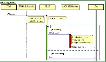
3.4 Event triggered control
Event triggered control is a mechanism of triggering the control loop. Compared to the time
triggered control system, it only requires computation resources at the presence of some
factors. Considering the fact that the current drawn from power source may stay within a
introducing event triggered control can help reducing the computational resources required in
our system which is very important.
3.4.1 Introduction to event triggered control
As widely studied and taught, periodic control has been the main force in the implementation
of feedback control laws on digital platforms. However, questions related to periodic vs
aperiodic implementations have gone in and out of fashion since feedback control loops
started being implemented on computers (An Introduction to Event-triggered and
Self-triggered Control).
In order to illustrate concept and implementation of event triggered control, let’s consider a
discrete system
𝑥(𝑛 + 1) = 𝐴𝑥(𝑛) + 𝐵𝑢(𝑛)
Although we can arbitrary define our controller, a common used and representative linear
controller is assumed here as
𝑢(𝑛) = 𝐾𝑥(𝑛)
𝑢(𝑚 + 1) = 𝐾𝑥(𝑚 + 1)
𝑢(𝑚 + 2) = 𝐾𝑥(𝑚 + 2)
…
In event triggered control system, re-computing and updating of system input is done only
when the triggering fact appears. This means for
𝑝 > 𝑚 > 0
If the triggering event happens at and only at m and p, we have
𝑢(𝑚) = 𝐾𝑥(𝑚)
𝑢(𝑚 + 1) = 𝐾𝑥(𝑚)
…
𝑢(𝑝 − 1) = 𝐾𝑥(𝑝 − 1)
𝑢(𝑝) = 𝐾𝑥(𝑝)
𝑢(𝑝 + 1) = 𝐾𝑥(𝑝)
…
In fact, we can only compute input once, register it and use that input until the triggering
event occurs. This completely eliminates computational resources used when no event
3.4.2 Control algorithm execution time
Let’s consider the system with PI controller only which is a simple control form and
consumes less computational resources. With the code we have in 3.2.2.4, the execution time
of each ADC ISR is 1. 8us. Considering the fact that we are working on a 48 MHz micro
controller, the execution time of computing duty cycle is quite fast.
However, as the operating frequency of our system is 50 kHz, the percentage of CPU time
spent on controlling power source is
1.8𝑢𝑠
20𝑢𝑠 × 100% = 9%
This is acceptable, though not perfect, for our system. We can still use 91% of CPU time to
serve our application. But the problem is that embedded system would typically require
multiple voltage buses to operate. Some modules we used to test our system’s ability to drive
peripherals are shown in the table below.
Table 1 Load Module Operation Voltage
Consider we need 3 voltage buses, then 27% of CPU time is consumed to regulate the power
supply with the most simple control algorithm. This is way too much so we need to
implement event triggered control to further reduce CPU time utilized by regulating power
sources.
3.4.3 Sequence Diagram
First, let’s consider implementing event triggered control for system with only PI controller.
Compared to what we have for time triggered control system, the code doesn’t need to be
changed. We only need to change the triggering mechanism for our system.
The implementation of this mechanism used ‘windowed ADC’. The AD conversion will be
triggered by the beginning of all PWM signal but it will only generate an interrupt when the
output voltage is outside our bound. This bound is based on the reference voltage and does
not need to be updated.
Implementing event triggering mechanism is a bit different in terms of sequencing different
peripherals. With time triggered control method, we use the output voltage sensing ADC ISR
to trigger current control. This is not valid here because in event triggered system, the output
voltage sensing ADC ISR is not executed every period. And even though we do not want
current sensing ADC to generate ISR every period, we do want to sense and thus monitor the
output current every period so we can know the current change as soon as possible.
To address this problem, we used another count down timer to trigger current sensing ADC
every period and ensure the timing sequence. The sequence diagram is shown below (Figure
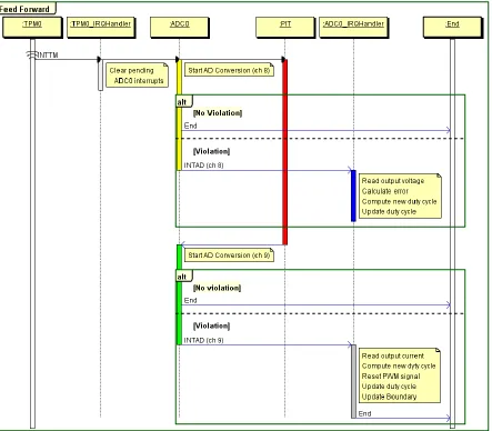
Figure 3-23 Event triggered feed forward control diagram
The beginning of every PWM signal will simultaneously trigger an output voltage sensing
AD conversion and a timer. This timer lasts long enough so even when voltage sensing ADC
ISR is triggered, it will expire after it is finished. This ensures that ADC will not get two
3.4.4 Sampling Position
Even though we can start another AD conversion when the previous ADC ISR is executing
and thus save some overhead, we don’t actually need to do that. To illustrate this, a typical
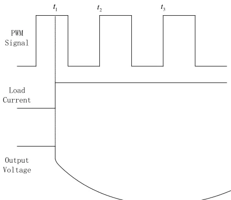
loading transient for buck converter is shown below (ripples are ignored).
PWM Signal
Load Current
Output Voltage
1
t t2 t3
Figure 3-24 Typical loading transient for buck converter
This is a very serious problem in our system because the majority voltage drop occurs during
the first two periods after the loading transient. This leads to the fact that no matter what
control algorithm we use, it’s impossible to reduce the maximum voltage drop because the
delay introduced by discrete sampling and updating. Consider the time between our current
sampling and the beginning of next PWM signal to be 𝑡𝑏 and period to be 𝑇, then the worst
case delay from the load transient occurs to the PWM signal respond to it is
𝑡𝑑𝑒𝑙𝑎𝑦 = 𝑇 + 𝑡𝑏
With this relationship, it’s obvious that decreasing 𝑇 and 𝑡𝑏 will help to decrease the overall
delay. For our system, 𝑇 is fixed. So we can only reduce 𝑡𝑏 which means to sample current
as late as possible in a period.
In our system, 𝑡𝑑𝑒𝑙𝑎𝑦 is capped at
𝑡𝑑𝑒𝑙𝑎𝑦 = 𝑇
Regardless of the value of 𝑡𝑏. This is achieved by implementing feed forward control and
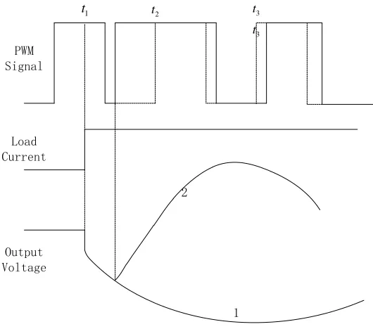
PWM Signal Load Current Output Voltage 1
t t2 t3
3 t
2
1
Figure 3-25 Loading transient for buck converter with feed forward and resetting
In our system, we update duty cycle and reset the PWM signal immediately after we detect a
load transient. Resetting PWM signal provides an immediate respond in control signal to the
load transient. A large pulse input is used to compensate for load transient and a much
smaller step input is fed into the system to deal with steady state output voltage drop caused
by resistance.
current sensing happens. So we don’t have to worry about how long the PIT timer should
take to expire because that wouldn’t influence the performance of our system.
3.4.5 Event triggered source code
The ADC ISR source for event triggered PI controller is no different from time triggered PI
controller. Actually we are not doing anything different. The only difference is how we
trigger the control loop to run and that’s done by different settings (windowed ADC). The
TPM ISR (shown below) is modified to set the boundary as well as triggering ADC.
NVIC_ClearPendingIRQ(ADC0_IRQn); TPM0->SC|=TPM_SC_TOF_MASK;
ADC0->SC2 |= ADC_SC2_ACFE_MASK|ADC_SC2_ACREN_MASK; ADC0->CV2=Upper;
ADC0->CV1=Lower; ADC0->SC1[0] = 0x48;
The setting of ADC boundary can be done in initialization code for only once which will
save interrupt time. But considering we have only one ADC module and it may be used for
other purpose, we are doing this setting in ISR for safety reason.
The ADC ISR for feed forward control with event triggered mechanism is a bit different
because we are not triggering the current sensing ADC at the end of our voltage sensing ISR.
The triggering mechanism is replaced by a countdown timer. The new ADC ISR source code
is shown below.
}
Compared to the ADC ISR we have for time triggered control, the only difference is we are
not triggering the AD conversion for current sensing with voltage sensing ADC ISR. Instead,
the TPM ISR will trigger another countdown timer (implemented with PIT module) as well
as voltage sensing ADC. The new TPM ISR is shown below.
NVIC_ClearPendingIRQ(ADC0_IRQn); TPM0->SC|=TPM_SC_TOF_MASK; channel=8;
ADC0->SC2 |= ADC_SC2_ACFE_MASK|ADC_SC2_ACREN_MASK; ADC0->CV2=Upper;
ADC0->CV1=Lower; ADC0->SC1[0] = 0x48;
PIT->CHANNEL[0].TCTRL |= PIT_TCTRL_TEN_MASK; The ISR for PIT is shown below.
NVIC_ClearPendingIRQ(PIT_IRQn);
PIT->CHANNEL[0].TCTRL &= ~PIT_TCTRL_TEN_MASK; PIT->CHANNEL[0].TFLG &= PIT_TFLG_TIF_MASK; channel=9;
ADC0->SC2 |= ADC_SC2_ACFE_MASK|ADC_SC2_ACREN_MASK; ADC0->CV2=UpperBound;
ADC0->CV1=LowerBound; ADC0->SC1[0] = 0x49;
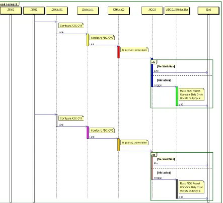
3.5 DMA triggered AD conversion
3.5.1 Introduction of DMA
Direct Memory Access (DMA) module is widely used in transferring data in high speed
application without MCU intervention. This may significantly reduce the interrupt triggered
and data registering done by MCU reduce MCU utilization.
In our system, the MCU communicate with peripherals by setting and reading registers. The
memory address of peripherals registers is compatible with data register memory and thus the
Considering the fact that the TPM interrupt and PIT interrupt in feed forward control are
triggered each PWM period and the work they do are configuring and triggering AD
conversion, we can use DMA to do the work to save MCU utilization.
3.5.2 Sequence Diagram
Figure 3-26 DMA Triggered Sequence Diagram
An additional timer TPM2 is used to trigger DMA twice each switching period. The
configuration and triggering of AD conversion are both done by DMA which saves MCU
3.5.3 DMA Source Code
The DMA only needs to go into interrupt to reset a counter every 2.62s. The configuration is
very important here. The source code for configuration DMA is shown below.
UpperBounds[0]=Upper1; UpperBounds[1]=Upper2; UpperBounds[2]=Upper1; UpperBounds[3]=Upper2; LowerBounds[0]=Lower1; LowerBounds[1]=Lower2; LowerBounds[2]=Lower1; LowerBounds[3]=Lower2; Channels[0]=0x48; Channels[1]=0x49; Channels[2]=0x48; Channels[3]=0x49;
SIM->SCGC7 |= SIM_SCGC7_DMA_MASK; SIM->SCGC6 |= SIM_SCGC6_DMAMUX_MASK; DMAMUX0->CHCFG[0] = 0;
DMA0->DMA[0].DCR = DMA_DCR_SSIZE(0) | DMA_DCR_DSIZE(0) | DMA_DCR_ERQ_MASK | DMA_DCR_CS_MASK |
DMA_DCR_SINC_MASK | DMA_DCR_SMOD(1) | DMA_DCR_LINKCC(2) | DMA_DCR_LCH1(1);
NVIC_SetPriority(DMA0_IRQn, 128); // 0, 64, 128 or 192 NVIC_ClearPendingIRQ(DMA0_IRQn);
NVIC_EnableIRQ(DMA0_IRQn);
DMAMUX0->CHCFG[0] = DMAMUX_CHCFG_SOURCE(56);
DMA0->DMA[0].SAR = DMA_SAR_SAR((uint32_t) (UpperBounds)); DMA0->DMA[0].DAR = DMA_DAR_DAR((uint32_t) (&(ADC0->CV2))); DMA0->DMA[0].DSR_BCR = DMA_DSR_BCR_BCR(0xffff0);
DMA0->DMA[0].DSR_BCR &= ~DMA_DSR_BCR_DONE_MASK; DMAMUX0->CHCFG[0] |= DMAMUX_CHCFG_ENBL_MASK;
NVIC_EnableIRQ(DMA1_IRQn); DMAMUX0->CHCFG[2] = 0;
DMA0->DMA[2].DCR = DMA_DCR_EINT_MASK | DMA_DCR_SSIZE(0) | DMA_DCR_DSIZE(0) | DMA_DCR_ERQ_MASK | DMA_DCR_CS_MASK | DMA_DCR_SINC_MASK | DMA_DCR_SMOD(1);
DMA0->DMA[2].SAR = DMA_SAR_SAR((uint32_t) (Channels));
DMA0->DMA[2].DAR = DMA_DAR_DAR((uint32_t) (&(ADC0->SC1[0]))); DMA0->DMA[2].DSR_BCR = DMA_DSR_BCR_BCR(0xffff0);
DMA0->DMA[2].DSR_BCR &= ~DMA_DSR_BCR_DONE_MASK; DMAMUX0->CHCFG[2] |= DMAMUX_CHCFG_ENBL_MASK; NVIC_SetPriority(DMA2_IRQn, 128); // 0, 64, 128 or 192 NVIC_ClearPendingIRQ(DMA2_IRQn);
NVIC_EnableIRQ(DMA2_IRQn);
2 DMA channels are assigned to transfer data to configure ADC and 1 channel is assigned to
trigger ADC. The triggering channel is linked to the end of configuration channels so it won’t
CHAPTER 4
EXPERIMENTS
In this chapter, simulations as well as experiments are done to show the effect of different
control algorithm and mechanism. I would introduce the setup of the experiments and show
the results.
4.1 Experiment settings
The synchronous buck converter shown in figure 3-1 is used to do experiments on.
Parameters for it is shown in table 2. I have also done simulation for the buck using the same
parameters as in real circuits. The simulation diagram shown in figure 3-2 is too simple to
represent the actual model. So I built a new model (Figure 4-1) with PLECS considering the
series resistance of some components and the new model gives a good understanding about
Table 2 Buck converter parameters
Vg Input Voltage 5V
L Inductance 68uH
C Output Capacitor 33uF
Ro Load Resistance 11.3Ω
Rl Inductor ESR 0.0.025
Rc Capacitor ESR 0.6
I Constant Current Source --
4.2 Constant current source
When people talk about buck converter, they typically use a resistor to represent the load.
However, a resistor load will lead to the fact that at transient time, the output voltage
transient will also cause load current transient and thus cause interaction between them. This
will lead to misunderstanding of the load transient. In our experiments, we used constant
current source (Figure 4-2) to act as the changing load and a constant load resistor to keep the
converter work in CCM. We would still have interaction between current and voltage
The current drawn by this circuit is either 544 mA (when load switch signal is high) or 140
mA (when load switch signal is low). This indicates a load transient of 404 mA. The current
drawn from power source is shown in Figure 4-3.
Figure 4-3 Load current transient
This is a very heavy load current transient for embedded system which will cause the output
voltage to be vary a lot. In real systems, large power-consuming turning on or off peripherals
such as WIFI module or a combination of different peripherals will lead to a similar load
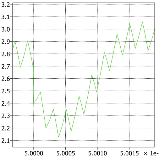
Note also that although there are ripples in the output which are caused by limited ability of
LM324 and power source. We can attenuate those ripples with methods such as adding
parallel capacitors. In my experiments, these ripples are left there on purpose because it
resembles real application more than constant current without ripples.
4.3 Feedback Control Result
With only feedback control, the PLECS model is constructed as Figure 4-4.
Figure 4-5 Simulated output voltage when load transient occurs
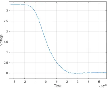
The simulated output voltage when transient occurs is shown in Figure 4-5. A maximum of
0.45V voltage drop occurs after 2 periods. The majority of voltage happens during the first
period after load transient occurs. In comparison, output voltage of our real buck converter is
Figure 4-6 Output voltage of buck converter when load transient occurs
The maximum voltage drop is 0.62V. The difference between simulation and hardware is
caused by inaccurate modeling of the parameters of components such as capacitance,
inductance and ESR of capacitor and inductor.
Besides output voltage variance, computational resources consumed in updating duty cycle
for PWM signal is another concern. Figure 4-7 shows PWM signal fed into high side
Figure 4-7 Computational resources consumed by updating duty cycle
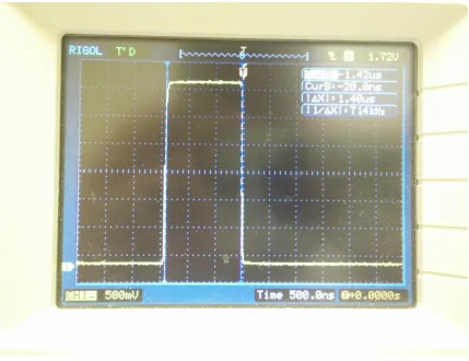
We can see that in each period, the control loop runs once and it takes 1.6 us each time to
execute. Here, as we only have one ADC channel to trigger, we don’t need to re configure
the ADC module. The ADC module is triggered by PWM signal once each period. Note that
the control loop running isn’t triggered by either the rising edge or the falling edge. This is
because we are using center aligned PWM signals. The beginning of each period is neither
the rising edge nor the falling edge but somewhere between the previous falling edge and the
next rising edge. So channel 2 and channel 1 in Figure 4-8 doesn’t seem to be aligned but it
actually is.
4.4 Feed Forward Control Result
The simulated output voltage when transient occurs is shown in Figure 4-10. A maximum of
0.22V voltage drop occurs after 2 periods. Compared with Figure 4-6, the maximum voltage
drop is reduced by 0.2V which is almost half of the maximum voltage drop.
Figure 4-10 Simulated output voltage when load transient occurs with feed forward control
Figure 4-11 Output voltage when load transient occurs with feed forward control
Ignoring the ripples caused by long wires, the maximum voltage is 0.4V. Around 1/3 of the
Figure 4-12 Simulated output voltage when load transient occurs with feed forward control
delayed
Figure 4-13 MCU utilization by updating duty cycle in each period with feed forward
control
4.5 Event triggered Control Result
A simulation using dead zone to simulate event triggered control with only PI controller is
done in PLECS (Figure 4-14).
Figure 4-14 PLECS model for event triggered PI control
As dead zone module would output 0 when the measured output voltage error is within the
range, duty cycle is not updated when the event (output voltage is not within the range)
Figure 4-15 Simulated output voltage when load transient occurs with event triggered
control
Compared with Figure 4-5, the maximum output voltage doesn’t change much (0.42V vs
0.45V). But the average output voltage changed by 0.1V due to the event triggered control
won’t update duty cycle if the output voltage is within 2.6V-2.8V range. In my circuit,
Figure 4-16 Output voltage when load transient occurs with event triggered control
Here, output voltage variance below the magnitude of 0.081V is ignored. The maximum
Figure 4-17 MCU utilization with event triggered control
Only when the output voltage is outside the range will the voltage sensing ADC trigger the PI
Figure 4-18 Number of ISR triggered when current changes
According to figure 4-18, 23 ISR is triggered to regulate the output voltage.
Figure 4-19 PLECS model for event triggered PI control with feed forward control
Figure 4-20 Simulated output voltage when load transient occurs with event triggered and
feed forward control
In my circuit, both the output current sensing ADC channel and the output voltage sensing
ADC channel use windowed ADC. At the beginning of each PWM duty cycle, PWM ISR is
triggered and ADC configuration registers are set for output voltage sensing. The PWM ISR
will also trigger a countdown time which will configure and trigger current sensing ADC
channel after the output voltage sensing ADC ISR is finished. The output voltage is shown
Figure 4-21 Output voltage when load transient occurs with event triggered feed forward
control
Figure 4-22 MCU utilization with event triggered feed forward control
Compared with section 4.4 when time triggered mechanism with feed forward control is
implemented, the output voltage sensing ISR is eliminated when output current doesn’t
change. An additional current sensing ISR (2 us each time executed) is executed once the
output current changes. But the TPM ISR and PIT ISR are added every period to set ADC
configuration registers. Figure 4-23 shows the number of ADC ISR triggered once the output
Figure 4-23 MCU utilization with event triggered feed forward control
According to Figure 4-22, 21 output voltage sensing ADC ISR and 1 output current sensing
Figure 4-24 Outpot voltage and MCU utilization with DMA
24 output voltage sensing ADC ISR and 1 output current sensing ISR is triggered when the
output current changes. The maximum voltage drop is 0.45V.
4.7 Task blocking impact
In real time system, the ISR can be blocked which causes additional delay in system’s
response. In my system, the signal that’s used to switch the load is also used to simulate the
will trap the MCU there with a dummy loop. The ISR used for updating PWM duty cycle is
thus blocked.
On the other hand, the maximum voltage drop is selected to measure the impact of blocking
time because it set the bounds for lowest operating voltage which determines power
consumption.
With my system and load current, the maximum voltage for feedback only control doesn’t
change with or without delay. This is because the maximum voltage drop is determined by
the open loop characteristic and the gain feedback controller is limited by stability and thus
isn’t reducing the maximum output voltage drop.
When the feed forward controller is delayed, more voltage drop occurs when longer delay is
introduced. Considering the time for AD conversion and ISR overhead, the minimum delay
between the load current changes and the feed forward controller work is 4 us. The
Figure 4-25 Blocking time VS Maximum Voltage Drop
The maximum voltage drop increases when delay becomes longer. The maximum voltage
drop will not be larger than 0.62V which is the same as the closed loop control (and the open
loop characteristic).
4.8 Analysis
MCU utilization, maximum output voltage drop and the cost of system are the three main
concerns in this system. Figure 4-25 shows the MCU utilization versus maximum voltage
drop for our system with different control architecture. The period for load current is 87.2ms
Figure 4-26 MCU utilization VS Maximum Voltage Drop
Feed forward control would decrease the maximum voltage drop for our system. Event
triggered control, on the other hand, would significantly decrease the MCU utilization while
Table 3 Hardware required for 4 control architectures Control Architecture Time Triggered Feedback Time Triggered Feedforward Event Triggered Feedback Event Triggered Feed Forward
ADC Module 1 1 1 1
ADC Channel 1 2 1 2
Windowed
ADC
0 1 1 2
Current sensor 0 1 0 1
PWM module 1 1 1 1
PWM channel 2 2 2 2
PIT module 0 1 0 1
PIT channel 0 1 0 1
The implementation of feed forward control and event triggered mechanism requires
CHAPTER 5
CONCLUSION AND FUTURE WORK
5.1 Conclusion
In this thesis, a closed loop control system with PI controller is first implemented in
FRDM-KL25Z board to regulate the output voltage of a synchronous buck converter. Then I add a
output current feed forward controller to improve the transient response of the buck when
load current changes. Then event triggered mechanism is used to replace the time triggered
one to achieve lower MCU utilization.
1. With PI controller only, the output voltage variance is large because the PWM signal duty
cycle’s response to the output voltage change is slow. It’s only when the output voltage
variance’s absolute value and accumulate value goes up will the duty cycle change. This is
causing a long delay before the output voltage can go to the ideal value.
2. When we add an output current to duty cycle feed forward controller to the system, the
output variance is reduced when load current changes. As we change the duty cycle of PWM
signal immediately after we detect the load current change, the response is fast and the delay
is only caused by the inertia of the buck converter and the time required to detect the load
and some delay may be added because the system think the voltage change is small enough
to be ignored at the beginning. An additional output voltage drop is thus added to the system.
4. Using DMA to trigger AD conversion will not influence the maximum output voltage drop
of buck converter but it will reduce the MCU utilization significantly. As most of the MCU
utilization was caused by configuring and triggering AD conversion when we use feed
forward control, the used of DMA to configure and trigger AD conversion significantly
reduces the MCU utilization. This makes feed forward control as cheap as feedback only
control in terms of MCU utilization.
5.2 Future Work
A bottleneck for the performance of feed forward controller is the time required to detect the
output current change. As we are using digital sampling method, this is inevitable. But we
may use analog comparator which would be monitoring the output current constantly and
inform us about load current change faster than ADC sampling method. In this way, we may
REFERENCES
[1] Shaffer, Randall. Fundamentals of power electronics with MATLAB. Firewall Media,
2007.
[2] Laszlo, Balogh. A Practical Introduction to Digital Power Supply Control. Texas
Instruments, 2005.
[3] Shamim, Choudhury. Designing a TMS320F280x Based Digitally Controlled DC-DC
Switching Power Supply. Texas Instruments, 2005.
[4] Zach, Zhang. BUCK Converter Control Cookbook. Alpha & Omega Semiconductor, Inc,
2008.
[5] Raghavan, Sampath. Digital Peak Current Mode Control of Buck Converter Using
MC56F8257 DSC. Freescale Semiconductor, 2013.
[6] Avik Juneja. Embeddeding Power: A Real Time Approach in Incorporating Switching
Power Conversion within Low-Cost Embedded Systems. North Carolina State University
Preliminary Oral Examination, 2014.
[7] Huangfu Yigeng, Wang Bo, Ma Ruiqing, and Li Yuren. Comparison for Buck Converter
with PI, Sliding Mode, Dynamic Sliding Mode Control. Electrical Machines and Systems
[9] Shi, L., Mehdi Ferdowsi, and M. L. Crow. "Dynamic response improvement in a buck
type converter using capacitor current feed-forward control." IECON 2010-36th Annual
Conference on IEEE Industrial Electronics Society. IEEE, 2010.
[10] Dean, Alexander G., and James M. Conrad. "Creating Fast, Responsive and