Si Microwire-Array Solar Cells
Thesis by
Morgan Charles Putnam
In Partial Fulfillment of the Requirements for the Degree of
Doctor of Philosophy
California Institute of Technology Pasadena, California
2010
Dedication
Acknowledgements
The work presented in this thesis would not be possible without the numerous con-tributions and lessons learned from all of the wonderful people with whom I have had the chance to interact while at Caltech.
First and foremost, I must acknowledge my advisor, Harry Atwater, who welcomed me into his group five years ago. I did not fully appreciate at the time what a great privilege and opportunity this was. The Atwater group is full of people who are truly passionate about the possibility for their research to make a meaningful difference in the world around them. Have no doubts, this is a direct reflection of Harry. In particular, I would like to thank Harry for beginning to teach me the value of patience. Nate Lewis has served as an unofficial co-advisor in many ways throughout my time here at Caltech. In this role Nate has offered forth his extensive knowledge of electrochemistry and the English language. Equally importantly, Nate has helped me to realize that while one can dedicate themselves to saving the world, it is best not to sacrifice oneself to it. His love of his Mazda RX-7, windsurfing, and his rumored love of the coral reefs in Hawaii have all been subtle reminders of this to me.
In particular, I would like to thank Michael Kelzenberg for showing me again and again, despite my protests to the contrary, the cadence of science. (The list of lessons that I could thank Mike for is actually quite a bit longer.) Brendan Kayes for demonstrating to me that those who know the most don’t always speak the most. Shannon Boettcher for inspiring me to think like a chemist. Daniel Turner-Evans for reminding me how to be thoughtful when working as part of a team, and Michael Filler for teaching me how to write a scientific manuscript. I would also be remiss if I didn’t thank Yunbin Guan for displaying true patience.
In addition to my research, I spent a good part of a year at Caltech working with Mike Kelzenberg to organize the student-installation of a 14 kW solar array on the roof of the Thomas J. Watson Laboratories of Applied Physics. A number of people were critical to the success of this project and in particular I would like to thank John Onderdonk, Jim Cowell, Alta Fang, Andrew Gong, and Heidrun Mumper-Drumm.
There is also a cohort of people who have helped me to maintain a sense of self and to help me grow as a person during my time here. Dalziel Wilson, Yonathan and Maayan Schwarzkopf, Mary Laura Lind, Nathan Lamarre-Vincent, Emily Rosene, John McKeen, David Pekarek, John Delacruz, Emily Warren, Michael Deceglie, Michael and Jessica Kelzenberg, Dan Turner-Evans, Shannon Boettcher, Imogen Pryce, Ryan Briggs, Kenneth Diest, Matthew Dicken, Melissa Archer, Adele Tamboli, Deirdre OCarrol, Marina Leite, Krista Langeland, Sean Pang, Erik Schomburg, Julian Romero, Alex Romero, Lise Lahourcade, Alice Robie, Alex Gagnon, Leo d’Espaux, and of course the Atwater group.
Morgan Putnam
May 2010
Abstract
By allowing for the fabrication of flexible crystalline-Si (c-Si) solar cells that employ
∼1/100th the Si of a traditional wafer-based c-Si solar cell, while maintaining high
photovoltaic efficiencies, vertically aligned arrays of c-Si microwires provide a novel photovoltaic geometry that has the potential to dramatically reduce the cost of solar electricity. In this thesis we report on 1) the growth of Si microwire arrays, 2) the chemical and electrical characterization of Si microwire arrays, and 3) the fabrication of Si microwire-array solar cells.
Using the vapor-liquid-solid (VLS) growth mechanism in combination with pho-tolithographic patterning, vertically aligned arrays of Si microwires, with nominally identical heights and diameters, were fabricated over areas >1 cm2. Chemical
char-acterization of the Si wires was then performed using secondary ion mass spectrom-etry to measure the incorporation of the Au VLS-catalyst into the Si wire. The incorporation of the VLS-catalyst into the Si wires at its thermodynamic equilib-rium concentration suggested that the use of Cu as a VLS-catalyst was less likely to limit the photovoltaic performance of Si microwire-array solar cells. Switching to the Cu-catalyzed growth of Si wires, in-situ doping with BCl3 was used to demonstrate
control of the electrically active dopant concentration from 8 × 10¹⁵ to 4 × 10¹⁹ dopants cm−3. Scanning photocurrent measurements were then made to measure the
Contents
List of Figures xv
List of Tables xix
List of Publications xxi
1 Introduction 1
1.1 The Promise of Solar Energy . . . 1
1.2 Photovoltaics . . . 2
1.2.1 Market . . . 2
1.2.2 Technology . . . 3
1.3 Si Microwire-Array Solar Cells . . . 4
1.3.1 Initial Motivation . . . 4
1.3.2 Flexible c-Si . . . 7
1.4 Thesis Outline . . . 8
2 Vertically Aligned Si Microwire Arrays 9 2.1 Introduction . . . 9
2.2 Vapor-Liquid-Solid Growth . . . 10
2.2.1 Mechanism . . . 10
2.2.2 Growth Conditions . . . 10
2.3 Catalyst Deposition . . . 15
2.3.2 Photolithographic Patterning . . . 17
2.4 Array Growth . . . 19
2.5 Discussion . . . 24
2.5.1 Si Precursor . . . 24
2.5.2 Photolithography . . . 24
2.6 Conclusion . . . 26
3 Si Microwire Chemical Composition 27 3.1 Introduction . . . 27
3.2 Background . . . 27
3.3 Sample Preparation . . . 28
3.4 Secondary Ion Mass Spectrometry . . . 30
3.4.1 General Principles . . . 30
3.4.2 Analysis Conditions . . . 30
3.5 Secondary Ion Count Rates . . . 33
3.6 Surface Au Concentration . . . 34
3.7 Bulk Au Concentration . . . 36
3.7.1 Un-etched and Au-etched Wires . . . 36
3.7.2 Removing the Surface Au . . . 37
3.8 Axial Au Concentration Profile . . . 38
3.9 Discussion . . . 40
3.9.1 Au Surface Phase . . . 40
3.9.2 Bulk Au Concentration . . . 40
3.9.3 Implications for Solar Cells - Catalyst Choice . . . 41
3.10 Measuring B and P Concentrations . . . 41
3.11 Conclusion . . . 44
4 Doping of Si Microwires 45 4.1 Introduction . . . 45
4.2 Background . . . 45
4.2.2 Literature . . . 46
4.3 Thermal Dopant Diffusion . . . 46
4.4 In-Situ Doping . . . 49
4.5 Total Dopant Concentration and Electrically Active Dopant Fraction 53 4.6 Electrically Active B Concentration in Ni-Catalyzed Wires . . . 54
4.7 Conclusion . . . 56
5 Minority-Carrier Diffusion Lengths in Cu-Catalyzed Si Wires 57 5.1 Introduction . . . 57
5.2 Background . . . 57
5.3 Scanning Photocurrent Microscopy . . . 58
5.4 Diode Fabrication . . . 58
5.5 Minority-Carrier Diffusion Lengths . . . 60
5.5.1 Measurement Conditions . . . 60
5.5.2 Photocurrent Response . . . 61
5.5.3 Extracted Minority-Carrier Diffusion Lengths . . . 64
5.6 Proposed Surface Passivation Mechanism . . . 64
5.7 Surface Recombination Velocity . . . 66
5.8 Discussion . . . 67
5.8.1 Bulk Minority-Carrier Diffusion Length . . . 67
5.8.2 Interface Trap Density . . . 68
5.8.3 Implications for Solar Cells Catalyst Choice . . . 68
5.9 Conclusion . . . 69
6 Si Microwire-Array Solar Cells 71 6.1 Introduction . . . 71
6.2 Background . . . 72
6.3 Device Design . . . 72
6.3.1 p-n Junction Design . . . 72
6.3.2 Contacting Strategies . . . 73
6.4.1 As-Grown, Scatterer, and PRS Cell Types . . . 74
6.4.2 Starting Material . . . 75
6.4.3 p-n Junction . . . 76
6.4.4 Al2O3 Scattering Particles . . . 79
6.4.5 a-SiNx:H Passivation/Antireflection . . . 79
6.4.6 Ag Back Reflector Fabrication . . . 81
6.4.7 Transparent Dielectric . . . 81
6.4.8 Transparent Conducting Oxide . . . 84
6.4.9 Completed Cells . . . 85
6.5 Characterization . . . 86
6.5.1 Cell Area . . . 86
6.5.2 Dark J-V . . . 91
6.5.3 Light J-V and Photovoltaic Performance . . . 91
6.5.4 Photocurrent Mapping . . . 94
6.5.5 Spectral Response . . . 96
6.6 Discussion . . . 97
6.6.1 Photocurrent Response from the Growth Substrate . . . 97
6.6.2 Comparing Between Cell Types . . . 98
6.7 15% Efficient Solar Cells . . . 98
6.7.1 Short-Circuit Current Density (Jsc) . . . 99
6.7.2 Fill Factor (FF) . . . 99
6.7.3 Open-Circuit Voltage (Voc) . . . 100
6.8 Conclusion . . . 100
7 Outlook 101 7.1 The Potential of Si Microwire-Array Solar Cells . . . 101
7.2 Advanced Device Design . . . 102
7.3 Future Technologies . . . 103
7.4 Conclusions . . . 106
B Secondary Ion Mass Spectrometry 119
C Scanning Photocurrent Microscopy 129
D Si Microwire-Array Solar Cells 133
List of Figures
1.1 Wire-array solar cell. . . 5
1.2 Modeled efficiency of a wire-array solar cell . . . 6
1.3 Flexible c-Si . . . 7
2.1 Vapor-liquid-solid (VLS) Growth . . . 11
2.2 SiH4 VLS growth reactor . . . 13
2.3 SiCl4 VLS growth reactor . . . 14
2.4 Blanket VLS-catalyst deposition . . . 15
2.5 Wire growth from blanket VLS-catalyst deposition . . . 16
2.6 Photolithographic patterning of the VLS-catalyst . . . 17
2.7 The importance of a thermal oxide . . . 18
2.8 Wire growth from a patterned catalyst array using SiH4 . . . 20
2.9 Wire kinking during VLS-growth . . . 21
2.10 Wire growth from a patterned array of Au using SiCl4 . . . 22
2.11 Wire growth from a patterned arrays of Cu and Ni using SiCl4 . . . . 23
2.12 Reuse of the growth substrate. . . 25
3.1 Si wires for SIMS analysis. . . 29
3.2 Secondary ion mass spectrometry (SIMS) . . . 31
3.3 SIMS analyzed wires . . . 32
3.4 Secondary ion count rates . . . 33
3.5 Radial Au concentration profile . . . 35
3.7 Axial Au concentration profile . . . 39
3.8 Expected cell efficiency as function of the VLS-growth catalyst. . . . 42
3.9 Radial P and B concentration profiles. . . 43
4.1 Optimal base doping . . . 47
4.2 Thermal dopant diffusion . . . 48
4.3 Radial p-n junction fabrication using thermal dopant diffusion . . . . 49
4.4 This will show up in the list of figures. . . 50
4.5 Electrically contacting single wires . . . 50
4.6 Back-gated FET schematic . . . 51
4.7 Demonstrating p-type behavior . . . 51
4.8 Electrically active dopant concentration as a function of the BCl3 con-centration . . . 52
4.9 Resistance of Ni-catalyzed Si wires as a function of the BCl3concentration 56 5.1 Schematic of scanning photocurrent microscopy. . . 59
5.2 Rectifying diode behavior of an Al MIS contacted, p-Si wire used in minority-carrier diffusion length studies. . . 61
5.3 Minority-carrier diffusion length in the dark and under broad-area il-lumination. . . 62
5.4 Transient behavior of minority-carrier diffusion length. . . 63
5.5 Independence of minority-carrier diffusion length on the applied bias. 65 5.6 Proposed surface passivation mechanism. . . 66
5.7 The calculated effective minority-carrier diffusion length as a function of the surface recombination velocity and bulk minority-carrier diffu-sion length. . . 67
6.1 Continuous emitter geometry. . . 73
6.2 Contacting strategies . . . 75
6.5 Phosphorous diffusion profile. . . 79
6.6 Incorporation of Al2O3 scattering particles. . . 80
6.7 Wire tips after removal ofa-SiNxH. . . 80
6.8 Ag back reflector fabrication. . . 82
6.9 Wire array infilled with mounting wax. . . 83
6.10 Indium tin oxide coated wire array. . . 84
6.11 Indium tin oxide transmission. . . 85
6.12 Cross sectional SEM images of Si microwire-array solar cells. . . 87
6.13 Optical images of Si microwire-array solar cells. . . 88
6.14 Scanning photocurrent microscopy. . . 89
6.15 Measuring the active area of Si microwire-array solar cells. . . 90
6.16 Dark J-V of Si microwire-array solar cells. . . 92
6.17 Light J-V of Si microwire-array solar cells. . . 93
6.18 Photocurrent maps of Si microwire-array solar cells. . . 95
6.19 Spectral response of Si microwire-array solar cells. . . 96
7.1 Single-wire solar cells. . . 102
7.2 Multi-junction wire solar cells. . . 104
7.3 Wire-array water splitting devices. . . 105
A.1 SiCl4 reactor schematic. . . 117
B.1 SIMS sample holder. . . 120
B.2 SIMS sputtered volume . . . 123
B.3 Decay of measured Au concentration. . . 125
B.4 Secondary ion count rates for different sputtering conditions. . . 127
D.1 Cracking of ITO on PDMS. . . 138
D.2 EVA infilled wire arrays. . . 140
List of Tables
4.1 Boron concentration measured by ICP-MS. . . 54
5.1 Calculated Ln,ef f in 2.0 µm diameter p-Si wires with a doping of 1.0×1017cm−3 for values of the surface recombination velocity (SRV) from 10 to 106 cm s−1 assuming a 20µm bulk minority-carrier diffusion length,Ln. . . 68
6.1 Photovoltaic performance under simulated AM 1.5G illumination. The champion solar cell from each cell type is bolded. . . 93
C.1 Calculation of the optical carrier generation density under laser illumi-nation. . . 130
C.2 Calculation of the optical carrier generation density under broad-area illumination. . . 131
D.1 As-Grown Cells (Voc and FF) . . . 134
D.2 Scatterer Cells (Voc and FF) . . . 135
List of Publications
Portions of this thesis have been drawn from the following publications:
Si Microwire-Array Solar Cells. M. C. Putnam, S. W. Boettcher, M. D. Kelzenberg, D. B. Turner-Evans, J. M. Spurgeon, E. L. Warren, R. M. Briggs, N. S. Lewis, and H. A. Atwater, Energy and Environmental Science, In press (2010).
10 µm Minority-Carrier Diffusion Lengths in Si Wires Synthesized by Cu-Catalyzed
Vapor-Liquid-Solid Growth. M. C. Putnam, D. B. Turner-Evans, M. D. Kelzenberg, S. W. Boettcher, N. S. Lewis, and H. A. Atwater, Applied Physics Letters,95, 163116 (2009).
Secondary Ion Mass Spectrometry of Vapor-Liquid-Solid-Grown, Au-Catalyzed, Si
Wires. M. C. Putnam, M. A. Filler, B. M. Kayes, M. D. Kelzenberg, Y. Guan, N. S. Lewis, J. M. Eiler and H. A. Atwater, Nano Letters, 8, 3109 (2008).
Growth of Vertically Aligned Si Wire Arrays over Large Areas (>1 cm2) with Au and
Chapter 1
Introduction
1.1
The Promise of Solar Energy
Solar energy is abundant, globally distributed, and free. Take a moment to consider the implications of this statement: energy, the single resource that has been most fundamental to improved standards of living, distributed equitably to all.
To place the abundance of solar energy in perspective, 90,000 terawatts (TW) of solar power continuously strikes the earth’s surface.[1] Humanity’s global power demand is a mere 14 TW.[2] Additionally, solar energy is the only energy resource that humanity could chose to use, not for the next 100 years, 10,000 years, or 1,000,000 years, but rather, for the next 5,000,000,000 years.
However the challenges to humanity’s use of solar energy are not without merit. Like the facts above, it is also no secret that we desire to use energy when the sun does not shine. Additionally, we have developed technologies (airplanes and automobiles) that require areal power densities that can not be directly met by solar energy. Finally, humanity is largely able to function through capitalistic economies, which may or may not have correctly assessed the cost of solar energy, in its present form, to be unaffordable.
1.2
Photovoltaics
Photovoltaic devices, or more commonly solar cells, are devices that upon exposure to electromagnetic radiation (photo) produce an electrical potential (volt). Though not the only means for harvesting solar energy†, photovoltaics are particularly interesting because of their ability to produce electricity, which is the largest and fastest growing form of energy used in the United States.[4]
1.2.1
Market
Photovoltaics are currently experiencing rapid global growth, with 10-year and 5-year compound annual growth rates of 46% and 56%, respectively.[5] This tremendous rate of growth was initially driven by the restructuring of Germany’s Renewable Energy Sources Act in 2000.[6] This act is a feed-in tariff, which guarantees to pay a price for photovoltaic electricity that will ensure that a well designed and operated photovoltaic system can realize between a 5 and 10% rate of return.
As the photovoltaics industry has grown, it has continued to exhibit a 80% progress ratio, which has led to significant cost reductions.[7, 8] A progress ratio reflects the cost reductions that are achieved as economies of scale are realized. Today the in-dustry appears to be between 6 and 10 years from grid-parity without technological breakthroughs.[9] Grid-parity is the point at which the end-user pays the same price for photovoltaic electricity as they would to purchase electricity from the electrical grid.
However, if photovoltaics are to move beyond simply providing electricity dur-ing the day, the cost of photovoltaic electricity must be reduced below the point
†Photosynthesis, concentrated solar power, and passive solar energy are also important methods
for harvesting solar energy. Though it receives little press, passive solar energy (the capture, storage
and use of solar energy through building elements such as windows, Trombe walls, sunrooms, thermal
chimneys, green roofs, roof ponds, thermal masses, day lighting and solar water heaters) is a form
of particular interest for reducing the 39% of U.S. annual energy consumption that is attributed to
of grid-parity. To this end the need for technological breakthroughs in the field of photovoltaics still exists.
1.2.2
Technology
A number of photovoltaic technologies exist in the market today, e.g. crystalline-silicon (c-Si), multi-crystalline crystalline-silicon (mc-Si), cadmium telluride (CdTe), copper in-dium gallium selenium (CIGS), amorphous-Si (a-Si), gallium arsenide (GaAs), and multi-junction solar cells, among others. Broadly, these technologies can be grouped into three groups. Thin-film technologies (CdTe, CIGS, a-Si) that are low-efficiency (7-10%) and low-cost (< $1 per Watt peak), c-Si and mc-Si solar cells that are mid-efficiency (13-22%) and mid-cost ($2.50-3.50 per Watt peak), and multi-junction solar cells that are high-efficiency (35-40%) and high-cost (many $100’s per Watt peak). Historically, crystalline-silicon (c-Si) and multi-crystalline (mc-Si) solar cells have been responsible for>90% of the photovoltaics market. But in recent years this frac-tion has dropped to ∼85% as thin-film technologies (specifically First Solar’s CdTe technology) have reduced costs low enough to enable significant market penetration despite their low efficiencies.
Despite these recent advances in thin-film technologies, c-Si and mc-Si photo-voltaics are still quite competitive with thin-film technologies because of their higher efficiencies. Though higher cell efficiencies are not enough to offset the low mate-rials and manufacturing cost of thin-film cells at the module level, the higher cell efficiencies of c-Si and mc-Si cells becomes economically significant at the systems level, where higher efficiencies allow for significant reductions in the installation and balance of systems (support structure, copper wiring, etc.) costs.
As follows below, we will present a technology that combines the reduced ma-terials utilization (and possibly the fewer number of processing steps) of thin-film technologies with the efficiencies of c-Si and mc-Si technologies.
1.3
Si Microwire-Array Solar Cells
1.3.1
Initial Motivation
For a typical photovoltaic installation, the solar panels comprise between 33% and 50% of the total installed cost.[9] In turn, for c-Si panels, the initial Si feedstock comprises between 14% and 28% of the panel cost.[10, 11] The large raw material cost of Si is determined by the purity of the Si required to produce efficient photovoltaic devices. Consequently, reducing the amount of Si feedstock required and/or the purity of the Si feedstock required‡has a significant impact upon the cost of c-Si solar panels and installed photovoltaic systems.
In order to reduce the Si purity required in a traditional wafer-based solar cell, one must decrease the distance that minority-carriers must travel before being collected at the p-n junction. However, because c-Si is a relatively weak absorber, the distance that minority-carriers must travel to the p-n junction is pre-determined by the wafer thickness required to absorb the incident illumination (∼200 µm). One design that circumvents this challenge is the use of radial p-n junctions in wire-array solar cells.[13]
‡Metallurgical grade Si (∼98% pure) can be purchased for∼$2/kg,.[12] while semiconductor/solar
As seen in Figure 1.1, the use of a radial p-n junction orthogonalizes the minority-carrier extraction direction from the light absorption direction. Si wires with length to diameter ratios on the order of 100:1 allow for solar cells that are optically thick, yet require minority-carrier diffusion lengths of only 1-2 µm, thereby significantly reducing the purity of the Si required.
n+-Si Shell
p-Si Core
hν
Figure 1.1. Schematic of a radial p-n junction, wire-array solar cell. Incident illumination is absorbed along the axial wire direction, while photogenerated minority-carriers (black dot) are collected radially.
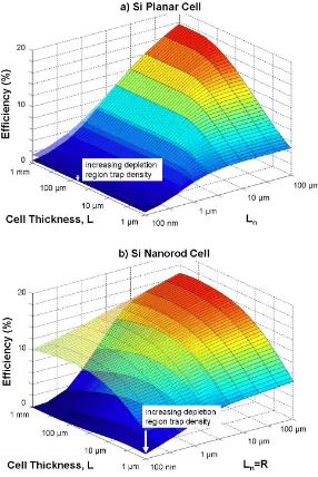
Figure 1.2 provides a comparison of the calculated solar cell efficiencies for (a) a traditional planar cell and (b) a wire-array solar cell, as predicted by numerical modeling.[13] Whereas the traditional wafer-based solar cell exhibits a significant decay in efficiency as the minority-carrier diffusion length (Ln) is reduced, the
Figure 1.2. Calculated cell efficiency as a function of minority-carrier diffusion length (Ln) and cell thickness for (a) a traditional
1.3.2
Flexible c-Si
Finding the predicted efficiencies of wire-array solar cells to be sufficiently high to merit further investigation, we began fabricating the proposed device structure. As will be detailed in Chapter 2, the fabrication of Si wire arrays is possible. However, we would like to point out that having fabricated Si wire arrays a fundamentally new type of material can be obtained by embedding the Si wire arrays in a flexible polymer.
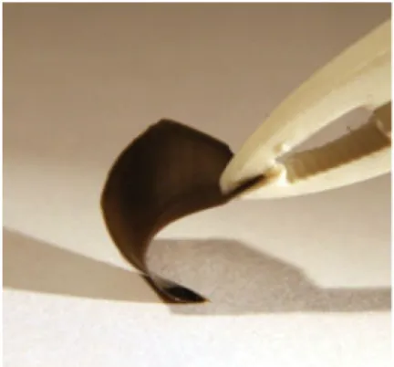
As can be seen in Figure 1.3, Si wires embedded in polydimethylsiloxane (PDMS) polymer are a flexible form of c-Si.[14] We have shown that this material can absorb
> 85% of the above bandgap solar illumination using a volume of Si equivalent to a 2.8 µm-thick Si film.[15] Thus, wire-array solar cells not only offer the possibility to reduce the cost of solar cells through the use of lower purity Si, but more importantly, wire-array solar cells offer the potential to use 1/100th the Si of a traditional
wafer-based solar cell. Furthermore, the flexibility of this material is especially exciting. In addition to allowing for the fabrication of flexible solar panels with efficiencies> 10%, it may also result in reduced module manufacturing costs through the adoption of quasi roll-to-roll fabrication processes.
1.4
Thesis Outline
This thesis will detail key steps in the fabrication and characterization of Si microwire-array solar cells. Chapter 2 will detail how the vapor-liquid-solid (VLS) growth mechanism can be used to grow arrays of nominally identical, vertically aligned, Si microwires over areas>1 cm2. In Chapter 3, Si microwires are chemically
Chapter 2
Vertically Aligned Si Microwire Arrays
2.1
Introduction
In this chapter we will discuss the development of a process for the fabrication of large-area arrays of vertically aligned, nominally identical, Si microwires. There are three major reasons that a homogeneous medium of Si microwires was felt to be important for the characterization and fabrication of Si microwire arrays as a potential photovoltaic material. First, control of the wire height and diameter allows for the fabrication of wires with diameters and heights that are optimized for photovoltaic performance based upon the measured photovoltaic properties of the wires. Second, fabrication steps, such as the definition of a p-n junction, the growth of a surface passivation layer, and the deposition of a transparent top contact, are much more straightforward (as will be seen in Chapter 6) for a uniform array of wires. Third, a large distribution of wire heights and diameters will lead to a distribution in each wire’s voltage at its maximum power point.[16] As the wires will be connected in parallel in a wire-array solar cell and as the wire-array solar cell must operate at a single voltage, a distribution in the wire height and diameter will result in a fraction of wires that operate away from their maximum power point. Thus, a wire-array solar cell with a large variation in wire heights and diameters will be inherently inefficient. The fabrication of nominally identical, vertically aligned, Si microwires was ac-complished through the use of the vapor-liquid-solid (VLS) growth mechanism. Pho-tolithography was used to pattern an array of VLS-catalysts (Au, Cu or Ni) onto a Si(111) wafer. VLS-growth using SiCl4 as a Si precursor at 1000 ◦C was then used
thermally grown silicon oxide was found to be critical to prevent catalyst diffusion and loss of pattern fidelity during the pre-growth anneal at 1000 ◦C.
2.2
Vapor-Liquid-Solid Growth
2.2.1
Mechanism
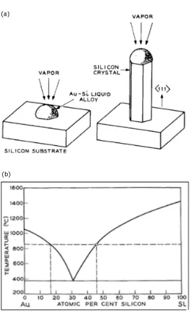
The vapor-liquid-solid (VLS) growth mechanism was discovered in 1964 by Wagner and Ellis.[17] As depicted in Figure 2.1, the VLS growth mechanism involves the incorporation of Si from a gaseous Si precursor into a VLS-catalyst/Si alloy (liquid), followed by the precipitation of solid Si from the VLS-catalyst/Si alloy. Under the appropriate growth conditions, the VLS-catalyst (most commonly Au) enhances the local deposition rate∼100-fold, resulting in the creation of a one-dimensional Si wire. Figure 2.1b provides the Au-Si phase diagram. Prior to the introduction of the Si precursor, Si from the growth wafer alloys with the Au catalyst (and Au from the catalyst diffuses into the wafer) as the sample is brought to the growth temperature. This annealing process results in a Au-Si alloy lying on the right liquidus line (as indicated by the small circle). With the addition of a gaseous Si precursor, the Au-Si alloy incorporates additional Si and begins to precipitate solid Si.
Studying the VLS-growth mechanism in some depth, Wagner and Ellis showed that a number of metals could be used as VLS-catalysts (e.g, Au, Pt, Ag, Pd, Cu, Ni, Gd, Mg and Os).[17, 19] Importantly, Wagner also showed that wires grown by the VLS-growth mechanism were single-crystals and grew in the <111> growth direction.[20] The observation of single-crystal wire growth is significant, as it indi-cates that the wires have the potential to exhibit very good photovoltaic properties.
2.2.2
Growth Conditions
For the fabrication of Si wires, the early work of Wagner focused on the use of SiCl4
(a)
(b)
typically range from 350-600◦C and have a typical SiH4 partial pressure between 0.01
and 5 Torr. SiCl4 growth conditions use temperatures between 800◦C and 1000◦C
and operate close to atmospheric pressure with a SiCl4 to H2 ratio of 1:50.
In addition to the different temperature and pressure regimes, a key difference be-tween the use of SiH4 and SiCl4 as a Si precursor is the presence of an etching reaction
when using SiCl4 as a Si precursor. The decomposition of SiH4 as shown in Eqn. 2.1
is an exothermic, irreversible reaction, limited only by kinetic decomposition.[24] In comparison SiCl4 can be used to either etch or deposit Si depending upon the
pres-sure, temperature, and the ratio of SiCl4 to H2 in the gas phase.[25] This is because
the decomposition of SiCl4 as shown in Eqn. 2.2 results in the production of HCl(g),
which is known to etch Si.
SiH4(g)→Si(s) + 2H2(g) (2.1)
SiCl4(g) + 2H2(g)Si(s) + 4HCl(g) (2.2)
In our work we have used both SiH4 and SiCl4 as Si precursors. For SiH4 growths,
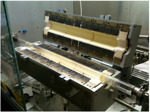
a hot wall reactor was used as shown in Figure 2.2, while for SiCl4 growths a tube
furnace reactor was used as shown in Figure 2.3. Using SiH4, Brendan Kayes found
the optimal growth temperature to be between 500 and 550◦C and the optimal growth pressure to be 1 Torr with a 100 sccm flow of SiH4 (5% in H2.)[26]. Using SiCl4 we
Figure 2.2. SiH4 VLS growth reactor located in Watson 247. The
Figure 2.3. SiCl4 VLS growth reactor located in Watson 251. Gases
2.3
Catalyst Deposition
2.3.1
Blanket Deposition
Initial efforts in our group to obtain Si wire arrays for solar cells focused on the blanket deposition (thermal evaporation) of Au catalyst, followed by the optimization of wire-growth conditions (catalyst, temperature and pressure) using SiH4 as the Si
precursor.[28] In this process, the blanket deposited Au would break up into smaller droplets from which the Si wires would grow, as schematically depicted and shown (for a 6 nm-thick Au layer) in Figure 2.4. It is clear from Figure 2.4c that the size of the Au-Si alloy at the onset of wire-growth was varied and that Si wire growth did not begin uniformly across the wafer.
375 nm (c)
(b) (a)
After three hours of growth, wire arrays exhibiting a roughly 75% fraction of vertically oriented wires were obtained, as shown in 2.5. The Si wires were ∼200 nm in diameter and on the order of 10 µm in length. In Fig. 2.5a, the short bright lines are the vertically oriented wires.
6.0 μm
4.3 μm
(a)
(b)
Figure 2.5. (a) Top-down and (b) tilted SEM images of a Si wire array grown from a 20 nm-thick Au film using SiH4 as the Si
2.3.2
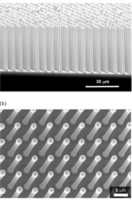
Photolithographic Patterning
Hoping to realize a more uniform array of Si wires, efforts were undertaken to pattern the Au catalyst prior to wire growth. Two photolithographic patterning processes were developed. The first process produced a square-array of 3µm diameter Au pads on a 7µm pitch on a Si(111) wafer (Fig 2.6a). The second process patterned the same array of Au pads, except that these pads were patterned onto the Si wafer through openings in a thermal oxide (SiO2) with the inverse pattern (Fig. 2.6b). Figures
2.6c,d provide optical and SEM images, respectively, of a catalyst array deposited onto a Si wafer through openings in a thermal oxide (the second process.) The right hand side of Fig. 2.6c is a region of the wafer with incomplete lift-off of the 1813 photoresist after blanket Au deposition. Though incomplete lift-off was not typical, it has been included here to provide a sense of the lift-off process.
21 μm
(b)
(d) (a)
(c)
Our initial thought in developing the second patterning process was that the etched oxide might guide initial wire growth in the vertical direction. However, given that SiO2 is etched isotropically by hydrofluoric acid (aq.) and that the deposited
catalyst thickness was comparable to the oxide thickness (typically 300 nm), it is un-likely that the patterned oxide conferred a significant physical barrier to wire kinking at the onset of growth. But, as can be seen in Figure 2.7, it was discovered that the presence of the thermal oxide between the patterned Au pads was critical to prevent-ing Au diffusion durprevent-ing the pre-growth anneal at 1000◦C when using SiCl4 as the Si
precursor.[27]
Figure 2.7. SEM images of patterned Au catalyst arrays before (left) and after (right) a pre-growth anneal in H2 (740 Torr) at 1000 ◦C.
2.4
Array Growth
As can be seen in Figure 2.8, use of the patterned catalyst arrays (no oxide present) in the SiH4 growth system resulted in the desired isolation of wire growth to areas
of the substrate initially patterned with catalyst (as expected from the VLS-growth mechanism.) Encouragingly, the density of wires and the fraction of vertically oriented wires was now uniform over the growth area, which was a marked improvement from the varying density of wires and varying fraction of vertically aligned wires obtained using the blanket deposition of catalyst (Fig. 2.5.)
However, the nucleation of multiple wires per patterned catalyst area and the presence of wire kinking during growth meant that the synthesized wire arrays were still not uniform enough for use in solar cells. The nucleation of multiple wires per Au pad is attributed to breakup of the catalyst droplet. Considering the large ratio of the catalyst diameter, 3000 nm, to the catalyst thickness, 1 nm, breakup of the catalyst droplet seems plausible. Furthermore, nucleation of multiple wires per Au pad was successfully eliminated by increasing the catalyst thickness to 300-500 nm. Figure 2.9 provides a higher magnification image of the kinking observed during wire growth.
While I had been working on the development of photolithographically patterned catalyst arrays, Brendan Kayes and Dr. Michael Filler had been building a reactor for VLS-growth using SiCl4. SiCl4 had recently been shown to yield a very high
fraction of vertically aligned Si wires,[28] and it was hoped that by combining the use of patterned catalyst arrays with a SiCl4 precursor we would be able to obtain
homogeneous wire arrays over large areas.
Indeed, as shown in Figure 2.10, the fabrication of nominally identical, vertically aligned, Si microwires over areas>1 cm2 was possible.[27] Though it was not known
(a)
(b)
4.0 μm
Figure 2.9. SEM image of a wire that has kinked multiple times during VLS-growth using SiH4 as a Si precursor.
observed wire diameter of 2µm is attributed to the change in the catalyst shape as it transitions from the solid state to the liquid state when alloyed with Si at the growth temperature.
(a)
(b)
Figure 2.10. (a) Cross-sectional and (b) top-down SEM images of a Si wire array grown in the SiCl4 reactor using a 500 nm-thick Au
(a)
(b)
2.5
Discussion
2.5.1
Si Precursor
Though our high-fidelity wire arrays were grown using SiCl4, it is not clear that similar
arrays could not also be grown using SiH4 as the Si precursor. However, the presence
of an etching reaction during SiCl4 growth should facilitate the removal of high-energy
surface defects that may lead to kinking during wire growth. Indirect evidence for the dependence of kinked wire growth on surface defects exists in the literature. Using SiH4 as the Si precursor, Westwater showed that wire kinking decreased with
in-creasing growth temperature and decreased with dein-creasing SiH4 partial pressure.[21]
Higher growth temperatures and lower SiH4 pressures should both result in greater Si
surface diffusion, the later as a result of a greater number of unoccupied surface sites. Thus, Westwater’s observations support the hypothesis surface defects may lead to kinked wire growth.
Additional indirect evidence relating wire kinking to surface defects is provided by two separate observations. First, Si wires grown from Si2H6 at a pressure of 1×10⁻⁶
Torr and temperature of 600◦C (using an ultra-high vacuum growth system) exhibited minimal kinking, while wires grown under the same conditions with the addition of 2 × 10⁻⁷ Torr O
2 exhibited significant wire kinking.[30] Second, O2 is known to
prevent the sintering of Si particles (performed at T > 1000 ◦C), which is largely a surface diffusion driven process.[31] Thus, we again conclude that decreased surface diffusion and a probable increase in the number of defect states at the Si surface is likely related to kinked wire growth.
2.5.2
Photolithography
in the Lewis group has demonstrated a promising method to re-use the growth sub-strates without additional patterning, as seen in Figure 2.12.[32] After peel-off of the PDMS-embedded Si wire array,[14] the growth substrate retains the patterned ther-mal oxide as well as a sther-mall fraction of the wire bases and the PDMS (Fig. 2.12a). The wire bases and the PDMS are then removed through wet chemical etching, while leaving the patterned thermal oxide intact (Fig. 2.12b). The desired array of Au cat-alyst pads was then created through the electrodeposition of Au, taking advantage oxide’s dielectric properties (Fig. 2.12c). Thus, another Si wire array was grown on a previously used growth substrate without the use of additional patterning methods (Fig. 2.12d).
2.6
Conclusion
Vapor-liquid-solid growth using SiCl4 as a Si precursor and photolithographically
Chapter 3
Si Microwire Chemical Composition
3.1
Introduction
Having demonstrated the ability to fabricate arrays of vertically aligned Si microwires using the vapor-liquid-solid (VLS) growth mechanism in Chapter 2, we turned our fo-cus to the characterization of the wires’ chemical composition. Quantitative measure-ment of the concentration of both impurity (e.g., VLS catalyst) and dopant species in Si microwires allows one to understand the limits on photovoltaic efficiency im-posed by the VLS growth mechanism and the pn-junction fabrication process. In this chapter we use secondary ion mass spectrometry to characterize the Au catalyst concentration within individual, VLS-grown, Si wires. For Si wires grown by chemical vapor deposition from SiCl4 at 1000◦C, an upper limit on the bulk Au concentration
was observed to be 1.7×10¹⁶atoms cm−3, similar to the thermodynamic equilibrium
concentration of Au in Si at the growth temperature. Additionally, we demonstrate the ability to measure B and P concentrations > 5 × 10¹⁷ atoms cm−3. Finally, we
discuss the motivation for switching to Cu-catalyzed wire growth.
3.2
Background
vapor deposition (CVD) at 550◦C using SiH4 as the Si precursor.[33] However, using
LEAP tomography Perea et al. were unable to detect Au in the Si wires and were limited to setting an upper limit on the Au concentration between 5 × 10¹⁷ and
1.5 × 10¹⁸ atoms cm−3.[34] More recently, high-angle annular dark-field (HAADF)
scanning transmission electron microscopy (STEM) has been used to spatially localize single Au atoms within 15 nm diameter Si wires grown by CVD at 450◦C,[34] as well as∼30 nm diameter Si wires grown by molecular beam epitaxy (MBE) at 500◦C.[35] SiH4 was used as the Si precursor in both reports. These HAADF STEM results
suggested that for both the CVD and MBE grown Si wires the bulk Au concentration is considerably greater than the thermodynamic equilibrium concentration of Au in Si at the growth temperature. Estimates of the bulk Au concentration from the HAADF STEM results were limited by the small volume of Si sampled (only a couple Au atoms were detected) and the correspondingly poor counting statistics.
3.3
Sample Preparation
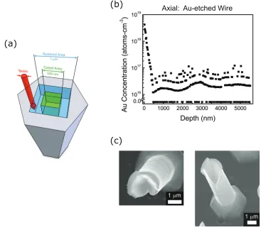
As described in Chapter 2 and shown in Figure 3.1, high-fidelity arrays of well-aligned Si wires were grown from patterned Au catalysts on a Si(111) wafer.[27] These wires were then analyzed in both the axial and radial directions. To analyze the wires radially, the wire arrays were sonicated in isopropanol to obtain a suspension of Si wires in isopropanol. This suspension was then drop-cast onto a Ge(111) wafer to obtain wires lying on their side. For axial analysis, wires were measured in their as-grown vertical orientation on the growth substrate.
(c)
(a)
(b)
Figure 3.1. VLS-grown, Au-catalyzed, Si wire arrays were grown on a Si(111) substrate from Au catalyst that had been lithographically patterned and confined by a thermal oxide. Wires were tens of mi-crometers in length and 2 µm in diameter and grew in the <111>
3.4
Secondary Ion Mass Spectrometry
3.4.1
General Principles
In secondary ion mass spectrometry (SIMS), a primary ion beam is used to ionize and sputter surface atoms from the sample, as depicted in Figure 3.2. The sputtered, ionized surface atoms (secondary ions) are then collected and analyzed in a mass spectrometer. To obtain accurate results, secondary ions are only collected from the center of the area over which the primary ion beam is rastered through the process of electronic gating (Fig 3.2a). Because it will be relevant to the discussion of the Au surface concentration later, it is worth noting that the process of sputtering produces an amorphized, well-mixed layer at the sample surface (Fig. 3.2b). In this work, a Cameca NanoSIMS-50L was used for secondary ion mass spectrometry (SIMS) analysis. The NanoSIMS-50L is a relatively new type of SIMS instrument (designed for use in the field of geology), which has the unique ability of being able to provide sub-micron spatial resolution.
To obtain an elements concentration (e.g., Au) from the secondary ion count rates, a relative sensitivity factor (RSF) is required, see Eqn. (3.1).
Au Concentration=RSF(atoms cm−3)
197Au count rate
30Si count rate (3.1)
The RSF is a function of the impurity and matrix secondary ion species sampled. To calculate the RSF, Au, B, and P standards (Charles Evans and Associates) with known Au, B, and P implant doses and depth profiles were used. A discussion of the calculated RSFs is presented in Appendix B.
3.4.2
Analysis Conditions
As a result of the complex ion optics necessary to achieve sub-micron spatial resolution in the NanoSIMS-50L, it was difficult to obtain similar beam conditions between suc-cessive sessions on the NanoSIMS. Optimal analysis conditions used a 1µm2 rastered
ra-(a)
(b)
Gated Area
Sample Rastered Area
dially profiled wire in Figure 3.3. Electronic gating of the secondary ions was used to further limit the area sampled to the center 0.25 µm2 of rastered area. However,
because the beam diameter has a finite size (on the order of a couple hundred nm) some secondary ions will be collected from outside of the electronically gated area. A discussion of the beam currents used and the resulting sample sputtering rates as well as the differences in analysis conditions can be found in Appendix B. For all measurements, wires were analyzed at normal incidence with a 16 keV Cs+ primary ion beam.
(b)
(a)
7.5μm
3.5
Secondary Ion Count Rates
The measured count rates of 30Si,74Ge, and 197Au secondary ions versus depth for a Au-etched Si wire analyzed in the radial direction are displayed in Figure 3.4. The point at which the sputtered depth reached the back surface of the wire was clearly visible from the sharp rise in the 74Ge count rate and the sharp fall in the 30Si count
rate. The197Au count rates within the bulk of the wires were often only a few counts per second (cps), but even a 1 cps 197Au count rate is still significant compared to
the average background 197Au count rate of ∼0.01 cps.
30Si
Radi
al
:
Au-
et
ched
Wi
r
e
Wir e-Substrate Interface
74Ge
197Au
Figure 3.4. 30Si, 74Ge, and 197Au secondary ion count rates for a radially profiled VLS-grown, Si wire. The vertical, grey band corre-sponds to the Si wire / Ge substrate interface, defined as the transi-tion region from 16% to 84% of the maximum counts for either30Si
or74Ge. The 30Si and74Ge count rates are referred to the left-hand y-axis, while the197Au count rate is referred to the right-hand y-axis.
than the back surface of the wires. This difference in the 197Au count rate produced
the observed difference in the front and back surface Au concentrations, see below. While the origin of the lower 197Au count rate at the back surface is unknown, we
suspect that the large aspect ratio of the sputtered crater when sampling the back surface leads to a decreased secondary ion extraction efficiency. At the same time, the sidewalls of the sputtered volume are likely to contribute a greater number of secondary ions as the sputtered depth increases. Thus the measured Au concentra-tion at the back surface is likely to have contribuconcentra-tions from both the back surface of the wire and the bulk of the wire. However, the difference in the 197Au count rate (and Au concentration) at the back surface may also be related to the discontinuous crystalline interface between the Si wire and the Ge substrate.
The second possible effect of the large sputtered depth to rastered length ratio was the roughly two-fold increase in the measured30Si counts as the wire was profiled in the radial direction. The increase in30Si counts is not well understood but may be
related to the effective increase in sputtering area as the sputtered depth increased. Remember that the finite width and Gaussian profile of the primary ion beam will result in the collection of some counts from outside of the electronically gated area, and thus allow for an increase in the effective sputtering area to be observed.
3.6
Surface Au Concentration
Figure 3.5 displays the Au concentration profiles for un-etched and Au-etched, radially profiled wires. In both cases, the Au concentration is larger near the surface than in the bulk (center) of the wires. Comparing the un-etched and the Au-etched wires, a large difference in both the near-surface and bulk Au concentrations was observed. As the Au removal does not appreciably etch Si, the differences between the two Au concentration profiles are ascribed to a difference in the amount of Au present at the surface of the wires before and after the Au etch.
(a)
Wir e-Substrate Interface Wir
e-Substrate Interface
Radial:Au-etched Wire Radial:Un-etched Wire
(b) (c)
to produce an exponential decay in the observed Au concentration profile. This is observed for the Au-etched wires, though a single exponential decay is less obvious for the un-etched wires. The perturbation from a single exponential decay for the un-etched wires is thought to arise from the use of a more diffuse primary ion beam during analysis of the un-etched wires (confer Appendix B).
Given the evidence for the observed near-surface Au concentration arising from Au on the sidewalls of the wires and a mechanism by which Au could be mixed to a greater depth within the wire, it is reasonable to estimate the surface Au concentration by integrating the Au concentration profile for the un-etched Si wire over the depth of the near-surface region (Fig. 3.5b). Integrating from 0 to 400 nm yields an estimate for the surface Au concentration on the order of 1 monolayer.
Further examining the observed surface Au concentration, one finds that it is larger at the front surface than at the back surface of the wires. This difference in the surface Au concentration seems unreasonable, given the radial symmetry of the wires. As discussed in Section 3.5, the high-aspect ratio of the sputtered volume when sampling the back surface of the wire may be producing this asymmetry in the surface Au concentration. It is important to note that the elevated Au concentration observed within the Ge wafer, seen for both un-etched and Au-etched wires, is an artifact of the decreased 30Si count rate when sputtering the Ge wafer.
3.7
Bulk Au Concentration
3.7.1
Un-etched and Au-etched Wires
a small fraction of secondary ions are being collected from outside of the rastered area. Given the high surface Au concentration, the collection of only one secondary ion in 200 from outside of the rastered area would produce the observed bulk Au concentration for the un-etched wire.
To obtain an estimate for the bulk Au concentration, the observed Au concen-tration was averaged over the first half of the Au-etched wires (not including the near-surface region), where the effects of the high-aspect ratio sputtered area should be smallest. For the five, Au-etched, radial profiles obtained, the average Au concen-tration within the bulk of the wire was 1.7±0.7×10¹⁶ atoms cm−3. The internal error of the measurement is estimated to be < 15%.† Given the high surface Au concentration still present for the Au-etched wires and the potential to collect counts from the sidewalls of the wires, the average bulk Au concentration is best viewed as an upper limit.
3.7.2
Removing the Surface Au
As seen in Figure 3.6, an increased Au concentration at the surface of the wire is not observed with the addition of a KOH etch after the Au-etch to remove ∼20 nm of the surface Si. For the two KOH-etched wires, the average bulk Au concentrations were 1.2 × 10¹⁶ atoms cm−3 and 0.9 ×10¹⁶ atoms cm−3, demonstrating that the bulk Au concentration is ∼1 × 10¹⁶ atoms cm−3. As before, the average was performed over
the first half of the wire. However, the un-rastered analysis conditions (Appendix B) used to measure the KOH-etched wires resulted in a larger internal error for the bulk Au concentration. Therefore, we believe that the Au-etched data reflects the most conservative upper bound on the bulk Au concentration.
†The total internal error is found by taking the root of the sum of the squares of the internal
errors. The two dominant internal errors arise from the counting statistics for the197Au secondary
Radi
al
:
KOH-
et
ched
Wi
r
e
Wir e-Substrate
Interface
Figure 3.6. Radial Au concentration profile for a KOH-etched, Au-etched, VLS-grown Si wire. Note the observed zero Au concentra-tion values in the Au concentraconcentra-tion profile. The vertical, grey band corresponds to the Si wire / Ge substrate interface, defined as the transition region from 16% to 84% of the maximum counts for either
28Si or 74Ge.
3.8
Axial Au Concentration Profile
Figure 3.7 depicts the Au concentration profile observed when a Au-etched, Si wire was axially profiled. For the wire shown, the observed Au concentration decreased exponentially from 6 × 10¹⁸ atoms cm−3 at the surface to an average of 2.4 × 10¹⁶ atoms cm−3 within the bulk of the wire, while a second axially profiled wire exhibited
a surface Au concentration of 8×10¹⁸atoms cm−3and an average bulk Au concentra-tion of 5 ×10¹⁶ atoms cm−3. As compared to the Au-etched, radially profiled wires,
simi-lar for both the axially and the radially profiled wires. Though the axially profiled wires exhibited a few-fold higher bulk Au concentration, the sputtering of the wire sidewall that occurred in the axial geometry, shown in Figure 3.7c, would be capable of producing this difference.
(b)
(c) (a)
Axial:Au-etched Wire
3.9
Discussion
3.9.1
Au Surface Phase
The increased Au concentration on the sidewalls of the wires may be a result of a Au-Si phase that is present during growth. The existence of a Au-Si phase on the sidewalls of VLS-grown, Au-catalyzed, Si wires during growth has been suggested previously for Si wires grown with Si2H6 as the Si precursor,[38] and Au clusters,
possibly indicators of the existence of a Au-Si surface phase, have also been found on the surface of Si wires grown with SiH4.[39, 40] Moreover, HAADF STEM results
also revealed an increased Au concentration near the sidewalls of the wires for the MBE grown wires, though not for the CVD grown wires.[34, 35] In our work, for the two un-etched wires measured, the integrated amount of Au over the surface region was on the order of 1 monolayer, which would be consistent with the existence of a Au-Si surface phase.[41]
3.9.2
Bulk Au Concentration
Our observed upper limit on the bulk Au concentration of 1.7 × 10¹⁶ atoms cm−3 is
comparable to the 1 × 10¹⁶ atoms cm−3 thermodynamic equilibrium concentration of Au in Si at the growth temperature of 1000 ◦C.[42] The observed upper limit represents a chemical sensitivity to Au in Si of ∼400 ppb. For the VLS growth method, the Au-Si phase diagram should determine the bulk Au concentration within the Si wire provided that the diffusion kinetics are sufficiently rapid to enable the establishment of the thermodynamic equilibrium Au concentration within the wire. Thus, we expect the bulk Au concentration within our 2 µm diameter Si wires to be representative of the bulk Au concentrations for Si wires ranging from tens of nm to manyµm in diameter, as long as the Au-Si phase diagram is similar across the range of diameters and the wires are grown under our growth conditions.
wires grown by CVD and MBE at temperatures of 450 ◦C and 500 ◦C, respectively, using SiH4 as a Si precursor.[34, 35] While these differences can not yet be fully
ex-plained, it is possible that they are related to changes in the growth temperature and/or the Au-Si phase diagram between the various growth conditions and wire di-ameters. In particular, the much higher temperature of our growth conditions should prevent kinetic effects from controlling the incorporation of the VLS-catalyst into the Si wire at concentrations other than the thermodynamic equilibrium concentration.
3.9.3
Implications for Solar Cells - Catalyst Choice
A bulk Au concentration of 1.7 × 10¹⁶ atoms cm−3 in Si is expected to yield a
minority-carrier recombination lifetime of 3 ns, for either electrons or holes as minority carriers.[42] In a radial-junction photovoltaic cell, with dopant concentrations of 1018
dopants cm−3for both the n- and p-type regions, a 3 ns minority-carrier recombination lifetime would lead to minority-carrier diffusion lengths of 1µm for both electrons and holes,[43] which agrees reasonably well with the 2 µm effective hole diffusion length that has recently been observed by scanning photocurrent microscopy on similar VLS-grown, Au-catalyzed, Si wires with ND = 1018 atoms cm−3.[44] As shown in Figure
3.8, theoretical modeling predicts that solar cells with efficiencies of 13.4% should be possible with minority-carrier diffusion lengths of 2 µm. However, if other VLS-catalysts are also incorporated at their thermodynamic equilibrium concentration in Si using our growth conditions, then the use of Cu as a catalyst should result in minority-carrier diffusion lengths of at least 10 µm,[45] enabling the possibility for 17.5% efficient solar cells.
3.10
Measuring B and P Concentrations
Figure 3.8. Theoretically modeled solar cell efficiencies as a func-tion of wire radius and diffusion length. Cells with the expected minority-carrier diffusion length for Cu-catalyzed and Au-catalyzed microwires are highlighted, assuming that the catalyst is incorpo-rated at its thermodynamic equilibrium concentration in Si at the growth temperature.
Wire-Substrate Interface
(a)
(b)
Wire-Substrate Interface
3.11
Conclusion
Chapter 4
Doping of Si Microwires
4.1
Introduction
This chapter discusses the use of thermal diffusion and in-situ doping to control the electrically active dopant concentrations in Si wire devices. Thermal dopant diffusion was found to work well for producing a large dopant concentration (∼1019 cm−3) at the wire surface, while in-situ doping with BCl3 allowed for the electrically active
dopant concentration to be varied from 8 × 1015 cm−3 to 4 × 1019 cm−3 in the as-grown wire. In-situ doping was critical for the study of minority-carrier diffusion lengths (Ch. 5.), and both in-situ doping and thermal dopant diffusion were essential for the fabrication of efficient Si microwire-arrays solar cells (Ch 6.).
4.2
Background
4.2.1
Optimal Base Doping
wires have large wire length to wire diameter ratios, ∼1/100.) However, if the base doping is too high (Fig. 4.1c), it can lead to a reduction of the minority-carrier dif-fusion length to the point where photo-generated minority-carriers recombine before reaching the p-n junction. In the case of degenerate (very high, > 1019 cm−3) base
doping, a tunnel-junction may form between the base and emitter, eliminating the rectifying properties of the p-n junction. Thus, precise control of the base doping is critical for ensuring an optimal base doping (Fig. 4.1b) so that undue recombination of the photo-excited carriers does not occur.
4.2.2
Literature
Thermal diffusion doping, in-situ doping, and ion-implantation have been used to dope Si wires.[22, 46, 47] In particular, in-situ doping has been studied using p-type (trimethylboron and diborane) and n-type (phosphine) dopants in Si wires grown using SiH4.[22, 48, 49] However, to the best of our knowledge, no comprehensive
doping studies have been undertaken for Si wires grown using a SiCl4 precursor.
4.3
Thermal Dopant Diffusion
Initial attempts to control the electrically active dopant concentrations in the Si wires were made using thermal dopant diffusion. As depicted in Figure 4.2, either B or P source wafers were placed in close proximity to Si wire arrays and then heated in a tube furnace to a temperature between 850-950 ◦C under a stream of N2.
During the thermal diffusion, either boric oxides or phosphorous oxides were trans-ferred to the Si wires. Upon adsorption to the Si, the boric or phosphorous oxide decomposes, resulting in the formation of free B and P atoms and a SiOx layer. As
was shown in Figure 3.8a, this produced a thin region of doping at the wire surface. As will be shown in Chapter 6, the creation of a n+-Si emitter through a thermal
phosphorous diffusion helped lead to the fabrication of efficient solar cells.
To create a uniform base doping, a thermal drive-in of the dopant species is
(a)
(b)
Emitter
Depletion Region
Optimal Doping
Heavy Doping Depleted Core
(c)
Tube Furnace
Figure 4.2. Schematic of B thermal dopant diffusion.
to ensure complete diffusion of the B atoms across the radius of the wire (or 3 hrs at 1100 ◦C for P species.) Though not desirable in a commercial process because of the costs associated with processing steps that require high-temperatures, a thermal drive-in is an effective method for producing a uniform base doping as was shown in Figure 3.9a.
(a) (b) (c) (d)
Intrinsic Si
Microwire Base Diffusion Base Drive-In Emitter Diffusion
Figure 4.3. Schematic of the radial p-n junction fabrication process using thermal dopant diffusion. Top, graphs of the net electrically active dopant concentration.
4.4
In-Situ Doping
To evaluate the possibility of in-situ doping, BCl3 was added to the SiCl4 and H2 gas
stream during the VLS-growth of the Si microwires. Upon the addition of BCl3 no
change in wire morphology or array fidelity was observed, as seen in Figure 4.4. By removing the wires from the growth substrate and depositing them onto a Si wafer with an insulating Si3N4 coating,[44] photolithographic patterning could be
used to deposit Al contacts on individual Si microwires for both 2 and 4-point current-voltage measurements, as shown in Figure 4.5.
Initial current-voltage measurements on the Si microwires grown in the presence of BCl3 were made in a back-gated field effect transistor geometry as shown in Figure
4.6. By applying a negative bias to the n+-Si substrate, a negative charge is introduced at the n+-Si/Si
3N4 interface and a positive charge is induced at the bottom surface of
50.0 μm
Figure 4.4. SEM image of a wire array grown with in-situ BCl3
doping.
n+-Si substrate, a negative charge is induced at the bottom surface of the wire. This
negative charge will produce a depletion layer in p-type Si microwires and result in a slightly increased wire resistivity. As seen in Figure 4.7, this is exactly the type of behavior we observe for Si microwires grown in the presence of BCl3.
VSource
VDrain
n+-Si Substrate Si3N4
Si Microwire
VApplied
Figure 4.6. Schematic of back-gated field effect transistor measure-ment.
Figure 4.7. Voltage-current behavior of a Si microwire grown with BCl3 in-situ doping.
the expected p-type behavior, four-point I-V measurements were used to measure the wire resistance as a function of the BCl3 concentration in the gas phase. Four-point
I-V measurements, as opposed to two-point I-V measurements, were made so that the contact resistance could be eliminated from the measured wire resistance. From the measured wire resistance and cross-sectional area (as measured by SEM), a wire resistivity was calculated. The wire resistivity was then used to infer the electrically active dopant concentration.[50]
Figure 4.8 plots the electrically active dopant concentration as a function of the BCl3 concentration in the gas phase. By varying the gas phase concentration
from 0.5 to 200 ppm, the electrically active dopant concentration could be varied from 8 × 1015 cm−3 to 4× 1019 cm−3. Cu-catalyzed, microwires grown without the presence of BCl3 were not observed to pass current under reasonable biases, implying
that any electrically active dopants were present in concentrations << 1014 cm−3.
Figure 4.8. Electrically active doping concentration as a function of BCl3 concentration in the gas phase. Error bars are the standard
4.5
Total Dopant Concentration and Electrically
Active Dopant Fraction
In addition to control of the electrically active dopant concentration, the demonstra-tion of a high electrically active dopant fracdemonstra-tion (electrically active dopant concen-tration / total dopant concenconcen-tration) is desirable. A low ( < 0.1) electrically active dopant fraction is undesirable as it will lead to increased carrier recombination with-out providing the desired electrical properties.
Initial attempts to measure the total dopant concentration were made using both secondary ion mass spectrometry (SIMS) and inductively coupled plasma mass spec-trometry (ICP-MS). Using SIMS an attempt was made to measure the B concentra-tion for two different doping concentraconcentra-tions. However, the analysis condiconcentra-tions chosen (an O− primary ion beam was used instead of the Cs+ primary ion beam in an at-tempt to measure the Cu concentration in Cu-catalyzed wires) did not result in the generation of enough secondary ions to quantitatively measure the B concentration.
in the ICP-MS measurement, and further development of ICP-MS sample preparation and data collection is necessary to obtain quantitative results.
Table 4.1. Boron concentration measured by ICP-MS.
598 599 600 601
[B] calculated from semi-quantitative analysis (cm−3)
5.0 × 10¹⁶ 1.5 × 10¹⁷ 4.0 × 10¹⁷ 1.3 × 10¹⁸
[B] calculated from concentra-tion standards and sample mass (cm−3)
2.2 × 10¹⁷ 5.0 × 10¹⁷ 1.3 × 10¹⁸ 4.0 × 10¹⁸
NA (cm−3) 4.0 × 10¹⁶ 6.7 × 10¹⁷ 2.8 × 10¹⁸ 1.0 × 10¹⁹
4.6
Electrically Active B Concentration in Ni-Catalyzed
Wires
The use of BCl3 as an in-situ dopant was also studied for Si wires grown from a
Ni-catalyst.[51] The Ni-catalyzed, Si wires were grown under the same growth conditions as the Cu-catalyzed, Si wires, and the preparation of single wire devices for electrical characterization (wire placement onto a Si wafer with an insulating coating, followed by photolithography, contact deposition and contact annealing) was also the same. However, unlike for the Cu-catalyzed wires, four point current-voltage measurements were only linear (and therefore meaningful) for the most heavily doped wires. For the most heavily doped, Ni-catalyzed wire an electrically active B concentration of 4 ×1017 cm−3 was inferred.
for the Ni-catalyzed wires grown under the highest BCl3 concentration, which
ex-hibited a significantly decreased resistance as expected), suggesting that the contact resistance was large and that it dominated the measured resistance. Modifications to the contact fabrication procedure (chemical etching prior to metal deposition, contact anneals of increased temperature and time) were made in an attempt to reduce the contact resistance, but no appreciable change in the measured resistances was ob-served. Though we do not know for sure, we suspect that the observed large contact resistances arose from a low electrically active B concentration in the wires (it can be quite difficult to obtain low resistance contacts to lightly doped,< 1015 cm−3, Si). If so this poses the curious question as to why the electrically active B concentration increased so dramatically between 10 and 45 ppm of BCl3 in the gas phase. One
Figure 4.9. Resistance of Ni-catalyzed Si wires as a function of the BCl3 concentration in the gas phase. Error bars are the standard
error.
4.7
Conclusion
In this chapter we have demonstrated the ability to controllably dope Si wires. Thru the combination of BCl3 in-situ doping to moderately dope the as grown Si wires and
Chapter 5
Minority-Carrier Diffusion Lengths in
Cu-Catalyzed Si Wires
5.1
Introduction
With the ability to control the active doping concentration in Cu-catalyzed, Si mi-crowires (Ch. 4), we turned our attention to the fabrication of devices that would allow us to study the minority-carrier diffusion length. As alluded to in section 3.9.2, the minority-carrier diffusion length is a critical indicator of material quality and plays a significant role in determining photovoltaic performance. To measure the minority-carrier diffusion length, scanning photocurrent microscopy measurements were made on single wire devices exhibiting rectifying behavior. In dark, ambient conditions, the effective minority-carrier diffusion length (Ln,ef f) was limited by surface
recombina-tion to a value of≤0.7 µm. However, a value ofLn,ef f = 10.5± 1µm was measured
under broad area illumination (low-level injection conditions). The minority-carrier diffusion length observed under broad-area illumination is consistent with filling of the surface states of the Si wires by photogenerated carriers and has important impli-cations for the design of high-efficiency solar cells from arrays of Si wires synthesized by the VLS-growth method.
5.2
Background
than the diffusion length in high-purity bulk Si. However, they are in good agreement with the minority-carrier diffusion length expected for Si with a Au concentration of 1.7 × 1016 cm−3, the measured Au concentration in the Si wires, see Chapter 3. (Au
is a highly effective recombination center in bulk Si.) As discussed in Chapter 3, the measured Au concentration in the Si wires is in good agreement with the thermody-namic equilibrium concentration of Au in Si at the growth temperature of 1000 ◦C. Assuming that the Cu concentration in the Si wire is also at its thermodynamic equi-librium concentration in Si at the growth temperature, Cu-catalyzed Si wires would be expected to exhibit bulk minority-carrier diffusion lengths of ∼20 µm.[45] Thus, by switching from the use of a Au VLS-catalyst to a Cu VLS-catalyst, we hope to see a significant enhancement in the bulk minority-carrier diffusion length.
5.3
Scanning Photocurrent Microscopy
As depicted in Figure 5.1, scanning photocurrent microscopy (SPCM) produces a map of a wire’s local photocurrent response by scanning the wire beneath a focused illumination source while the photocurrent is measured. For wires with a rectify-ing junction and sufficiently high doprectify-ing, such that the minority-carrier transport is dominated by carrier diffusion and not carrier drift, the minority-carrier diffusion length can be extracted using Eqn. (5.1), where (xJ xn-x) is the distance between the
rectifying contact and the laser illumination.[50]
Jph∝e
−(xJxn−x)
Ln,eff