Experimental and Numerical Investigations of Line-Shaped
Microwave Argon Plasma Source
Essam Abdel-Fattah1, 2, *, Haru Shindo3, Refat Sabry1, 4, and Alla E. Kotp1, 5
Abstract—In the following, numerical and experimental results for a line-shaped argon plasma source over a wide range of gas pressure (2–50 Torr) and microwave power (200–800 W) are presented. The line-shaped plasmas have been generated in a rectangular Pyrex tube, 15 mm in height and 5 mm inner width placed-in a linear slot made in the upper wide wall of a custom-made narrow rectangular waveguide. The microwave power is coupled to the discharge gas via the slot. The effects of the waveguide width, power level (electron density, and discharge tube insertion depth on the excited axial (along x) electric field profile and hence the uniformity of the produced plasmas are investigated numerically using commercial software CST Microwave StudioR, and charge coupled device (CCD) camera. Results showed that, a uniform line-shaped plasma is generated as waveguide width decreased to 58 mm, plasma density valuenres = 3.7×1011cm−3, and discharge tube insertion depth = 0 mm. An optical emission spectroscopy study was also realized to deduce the relative density of argon species and electron excitation temperatureTexc. In general, argon spectral lines intensity was increased enhanced markedly when microwave power increased, while the different lines showed different behavior as argon pressure increased. The electron excitation temperatureTexc decreases with increasing argon pressure, but almost constant overall the whole plasma length.
1. INTRODUCTION
There has been a great need for large area high-density plasma sources ( 30 cm length) for giant material processing. Typical examples for giant plasma processing are flat panel displays (FPDs), thin-film solar cell batteries, and surface modification of paper and organic thin-films to give either hydrophobic or hydrophilic properties [1]. Major specifications required for the plasma sources in such processing include a) high-density plasma production with low plasma potential for high throughput and quality processing, b) controllability of plasma profile to ensure uniformity over large-areas. Therefore many efforts have been focused to scaling up the conventional plasma sources toward ultra large size. For example very high frequency VHF capacitively coupled plasma was proven to produce high-density plasma. However, the existence of standing wave effect at large electrode diameter [2, 3] causes non-uniformity of the plasma profile. In addition, the problem of complete power transfer to the radio frequency RF discharge (i.e., the impedance matching problem)is inherent scaling up of such plasma source.
In contrast, microwave plasmas in particular surface-wave (SW) plasma, in which electromagnetic microwave coupled to the ambient gas through slot-antenna, is suitable for large area plasma generation at low gas pressure (< 10 mTorr) [4]. At low gas pressure, an axial uniform electric field distribution
Received 10 July 2015, Accepted 15 September 2015, Scheduled 18 September 2015
* Corresponding author: Essam Abdel-Fattah ([email protected]).
1 Physics Department, College of Science, Prince Sattam Bin Abdul-Aziz University, Al-Kharj, P. O. 83, Al-Kharj 11942, Saudi
may not be necessary to generate uniform long line-shaped plasma due to plasma diffusion. In contrast, the decrease of the mean free path length of the electrons at high gas pressure causes an inhomogeneous density of the plasma for large volumes or surfaces [5].
As known, microwave electric field distribution in the plasma determines the electron density, energy distribution and thus the homogeneity of the discharge. Therefore, the key problem is how to sustain a uniform and steady microwave electric field over large areas. A drawback of microwave (2.45 GHz) excitation is the non-uniformity of its electric field due to the relatively short wavelength (12 cm in free space). For microwave propagating in a rectangular waveguide, the guided wavelength λg
(excited mode TE10) is described as follows
λg = √1 εeff
λ0
1−
λ0 2·a
2, (1)
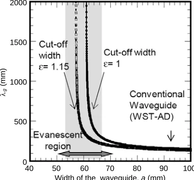
where a is the internal width of the waveguide and εeff the effective permittivity of the waveguide-discharge tube medium. Fig. 1 shows the computed guided wavelengthλgas a function of the waveguide widthaand the effective permittivityεeff. As inferred from Fig. 1, the guided wavelengthλgis relatively small and weakly dependent on the effective permittivityεeff for waveguide widths higher than 70 mm. However as waveguide width decreases, λg increase and strongly depends on the εeff. Also, we can observe that the effective permittivity is dependent on the waveguide widtha. For example in case of vacuum (r = 1) the cut-off width was about 61.3 mm which decreases to ∼ 57 mm as r increased to
1.15. In real waveguide based plasma system, εeff is far from unity and one should expect a tolerance geometrical cut off width. In other words, a long wavelength of an electric field to be excited in the waveguide is controlled by not only waveguide width, but also the effective permittivity εeff of the plasma-waveguide system, i.e., microwave power level (electron density), discharge tube insertion depth in the wave guidedins and plasma length/volume. Therefore, for an optimal line-shaped plasma design/operation, one should first examine the role of the device parameters and the plasma conditions and explore their possible influence on the axial distribution of the microwave electric fields profile.
In practice, optimization of a plasma source is performed experimentally on a cut-and-try basis, which is difficult and money/time consuming. In this situation, alternative tool is simulation instead of real experimental devices. However, modeling of microwave plasma is not an easy task; these plasma sources are complex systems in which large variety of modes can be excited [6]. Thus, computation with microwave analytical forced-oscillation approach [7] need some approximation for the spatial distribution of the microwave electric field in the coupling aperture and are, therefore, of little use for complex geometry’s, when such approximations are not readily available, since difference in the real and assumed
40 50 60 70 80 90 100
Width of the waveguide, a (mm) 2000
1500
1000
500
0
λ
(mm)
g
Figure 1. Calculated wavelength λg in the waveguide as a function of the waveguide widtha for two
excitation field profile may result in significant difference in the respective power absorbed. Fortunately, the electromagnetic fields and plasma parameters can probably estimated in surface wave plasma source, by using self-consistent computation of electromagnetic fields with kinetic plasma model [8] or a two-dimensional fluid model [9] for plasma evolution. However, such a hybrid simulation is practically conducted in one or two dimensions due to the limit of simulation time, while complex geometry such as line-shaped plasma needs to be modeled in three dimensions for optimizing the design and operation regime. Thus in this work, the electromagnetic microwaves is modeled using a commercial computer-based electromagnetic field simulation “CST Microwave Studio”. One of the advantages of the CST microwave studio is its ability to model complex geometries, of real plasma sources applied for plasma processing [10–13]. The software package is based on the finite integral method (FIM) representing a discrete analogue of Maxwell’s equations on a computational grid [14].
In this paper, a predictive 3D simulation to assist the optimal operation of the line-shaped microwave plasma source is presented. The model is used to investigate the uniformity of electric field in the waveguide/plasma, which we use as indicator for the plasma uniformity. The discharge is characterized by means of optical emission spectroscopy and CCD camera.
2. EXPERIMENTAL SETUP
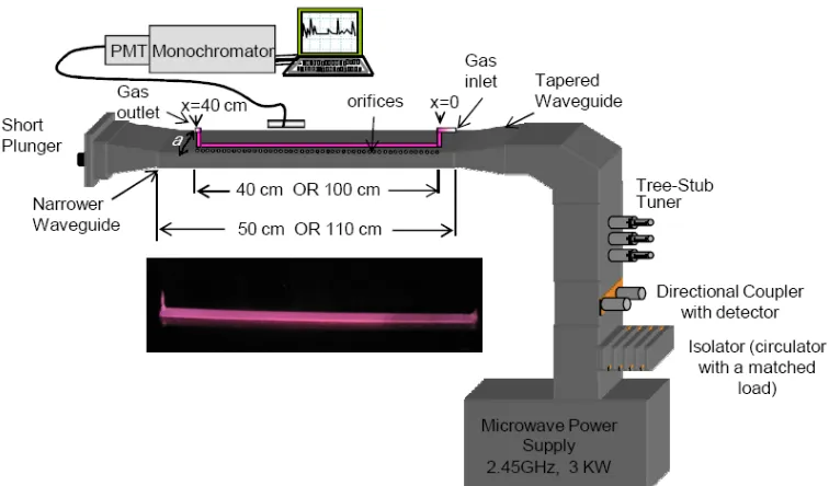
A schematic drawing of the experimental set-up is shown in Fig. 2. The line-shaped microwave plasma source consists of a 2.45 GHz microwave generator of maximum power 2 kW, a TE10 mode rectangular waveguide components (WST-AD standard) connected to custom-made narrow waveguide wave using tapered waveguide. The standard WST-AD waveguide was tapered off for low reflection transit to the custom-made narrow waveguide. This latter waveguide length was 50 cm (x = 0 cm to x = 50 cm) and it is internal width a could be varied by changing a detachable aluminum plate. The height of the custom-made waveguide was decreased to 5 mm in order to increase the electric field strength in the region of interest. To maintain the reflected power below 1% of the forward power, a three stub tuner and short plunger were used. The reflected power was deflected via a ferrite circulator into a high-power matched load connected to the circulator’s third port. The forward and reflected powers were monitored by directional coupler and detectors. The microwave power was coupled to the plasma through a linear slot, cut along the central line of the upper broad wall of the custom-made narrow waveguide. A rectangular Pyrex tube (pyrex = 4.82) of height 15 mm and inner width of 5 mm was
placed along the length of the slot, where the electric field intensity is at its maximum. The discharge tube was supplied with argon gas and the pressure was monitored using capacitance manometer.
For the determination of plasma parameters, optical emission of the line-shaped plasmas was collected by a collimated optical probe placed perpendicular to the Pyrex tube. An optical fiber was used to transmit the collected signal to the entrance slit of a monochromator (NIKON G250). The emission was amplified by a photomultiplier and then dispersed and analyzed by the monochromator (with a spectral resolution of 0.023 nm) in a preset wavelength range. The scanning and data acquisition process were controlled by the data acquisition and analysis software Spectra (Keyence NR-250).
3. RESULTS AND DISCUSSION
3.1. 3D Numerical Simulation of Line-shaped Plasma and Optimal Operating Regimes
For 3D numerical simulation, simulation was carried out for the frequency range of 2.0–2.8 GHz using transient solver of CST Microwave Studio. In the calculations, we rely on the Drude model to characterize the bulk plasma properties. Namely, the permittivity of cold collision plasma p is given
by
p = 1− ωp2
ω(ω+iνc) (2)
where ω is the microwave frequency, νc the momentum transfer collision frequency, and ωp the
plasma frequency ωp =
nee2
me0. Being non-consistent, our plasma model assumes plasma parameters
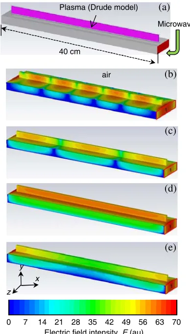
independent of the frequency and power of the exciting wave and also of the boundary conditions. Figure 3(a) shows a simplified 3D model for the 40 cm length line-shaped plasma source, which has the same dimensions and material as that of the real device (Fig. 2). All waveguide metal walls except the incoming wave port were assumed perfect conductors. The dielectric is loss-free, and the boundary condition outside the Pyrex glass is a free space. Microwave field is applied to the far end x-axis of the waveguide. The simulation results are obtained, using a pulse with frequency spectrum from 2.0 to 2.8 GHz, and picking up the Fourier component at the midpoint of 2.45 GHz. We are interested in plasma densities that represent different plasma behaviors in respect to microwave propagations. In other words, a) under-dense plasma density ne = 5.3×1010cm−3 (i.e., cut-off density nc = 7.4×1010cm−3, b)
non-resonance plasma density 9×1010cm−3 and 2.3×1011cm−3, c) surface wave resonance density
nres = 3.7×1011cm−3, and d) high-dense-resonance plasma density ne = 2.9 ×1012cm−3. In this investigation, we are interested in the field uniformity and the absolute strength of the field.
The computed electric field distribution (absolute value E =
E2
x+Ey2+Ez2) for various
waveguide widths are depicted in Figs. 3(b), (c), (d), (e) at the electron density ne = 9×1010cm−3 and the collision frequency νc = 3.7 ×10¹⁰Hz for argon pressure of 30 Torr. Here the line-shaped plasma model has 40 cm length, dins = 0 mm, and the x-axis is along the traveling direction. The color scale shown below the figure indicates the field intensity in arb. units. It is clear to see that the distributions of electric field strongly depend on the waveguide width. For example, at the standard waveguide width (a= 96 cm), there are several large high-electric-field regions periodically (the period of about 8 cm) distributed along the axial x direction, as can be seen in Fig. 3(b). This standing wave pattern of the computed electric field was found independent of the value of electron density (ne = 2.4×10¹⁰ ∼ 2.9×1012cm−3) and plasma volume (not shown). This localized excitation will
result in a non-uniform plasma profile along the x-axis. In contrast, for a narrow waveguide width
a = 62 mm, one can observe visually in Fig. 3(c) that λg of the computed electric field increases to
about 30 cm, whereλg is calculated from the node intervals of the standing waves formed in the narrow
0 7 14 21 28 35 42 49 56 63 70 Electric field intensity, E (au)
y
x
z
Plasma (Drude model)
Microwave
40 cm
air
(a)
(b)
(c)
(d)
(e)
Figure 3. (a) Model structure, and the computed electric field distribution along x axis at ne =
9×1010cm−3, νc = 3.7×10¹⁰Hz and insertion
depth dins = 0 mm, for various waveguide width (b) 96 mm, (c) 62 mm, (d) 58 mm, and (e) 55 mm.
0 7 14 21 28 35 42 49 56 63 70 Electric field intensity, E (au)
y x z
y x
z
(a)
(b)
(c) air Discharge tube
Waveguide port
ins
d
ins
d = 2 mm
ins
d = 5 mm
Figure 4. (a) Front view of model structure, and the computed electric field distribution along x
axis at ne = 9×1010cm−3, νc = 3.7×10¹⁰Hz,
and waveguide width of a = 58 mm for various discharge tube insertion depth, (b) dins = 2 mm, (c)dins = 5 mm.
along the plasma axis as seen in Fig. 3(d). Further decrease of the waveguide width ato values below 58 mm, for instance 55 mm, reduces the uniformity of the axial field profile as view in Fig. 3(e). Fig. 3, implies that uniformity of the excited electric field can be controlled by varying the waveguide width.
The effect of the discharge tube insertion depth dins on the electric field uniformity is also investigated. Fig. 4(a) shows a front view of the simulated model. Figs. 4(b), (c) show the axial (along x axis) distribution of excited electric for insertion depth (b)dins = 2 mm and (c) dins = 5 mm, respectively. Here, simulation was performed for a line-shaped plasma of total length 40 cm and has a waveguide width of a = 58 mm, electron density ne = 9×1010cm−3, and collision frequency
νc = 3.7×10¹⁰Hz that correspond to argon pressure of 30 Torr. One can observe visually in Figs. 4(b), (c) that increasing the insertion depth dins of the discharge tube deeper in the waveguide leads to shortening of the λg and hence a decrease in the line-shaped plasma uniformity. This behavior may
attribute to reflected waves due to imperfect coupling inside the cavity produced by the introduction of this asymmetry in the waveguide. Alternatively, increasing the insertion depthdins increases the effective permittivity εeff of the waveguide-plasma system and thus λg decreases, as predicted by Eq. (1).
In order to examine the effect of the microwave power level (electron densityne) on the uniformity
of axial electric field distribution, a 40 cm length line-shaped plasma model with waveguide width
30 Torr, as shown in Fig. 5. The electron density values were chosen to represent different plasma behaviors in respect to the microwave propagation. It can be seen that the change of ne alters the
axial (x) electric field distributions particularly for plasma densities higher than surface wave resonance density nres (nres = 3.7×1011cm−3). For example, at electron density value n
e 5×1010cm−3, the
axial distribution is uniform and a long period of electric field is observed. In contract, as electron density increases to 2.3×1011cm−3 or the higher density 3.7×1011cm−3, one can observe weakening of the electric field in the mid of the discharge tube as seen in Figs. 5(b), (c). Further increase of electron density to the higher value of 2.9×1012cm−3, results a completely non-uniform axial field and an interesting field patterns appears as seen in Fig. 5(d). The non-uniformity of the axial electric field at high electron densities may attribute to the skin effect; at electron density ≥ 3.7×1011cm−3 for instance, the collisional skin depth is 1.9 cm and is comparable to half the waveguide-plasma height. Thus, the microwave field does not penetrate deeper into plasma; instead it localized and propagates at the plasma-dielectric interface “surface waves SW”. A key point in our line-shaped plasma setup/model is that the discharge vessel made of glass. In case of glass discharge tube, however, SWs can be excited along all the interfaces between the glass wall and plasma: In fact, Figs. 5(a) through (d) clearly show that SW propagates not only horizontally along the waveguide axis (x-axis) but also vertically along the glass wall perpendicular to x-axis. This is differing than the case of discharge metal chamber in which the SW propagate only along the plasma-dielectric interface (near the slot) and hence one expect strong field only at the vessel bottom (near the slot). In conventional planar SW plasma source with annular slot and equipped by dielectric chamber, Siry et al. [16] observed experimentally the presence of surface waves propagating not only beneath the top quartz plate but also along the dielectric side
0 7 14 21 28 35 42 49 56 63 70 Electric field intensity, E (au)
(a)
(b)
(c) air
(d)
n = 5.3 × 10 cm10 -3
e
n = 2.3 × 10 cm
n = 3.7 × 10 cm
n = 2.9 × 10 cm e e e -3 -3 -3 11 11 12
Figure 5. Computed electric field distribution alongxaxis, at waveguide widtha= 58 mm,νc =
3.7×10¹⁰Hz and insertion depthdins = 0 mm, for various electron density (a) ne= 5.3×1010cm−3
(below cut-off density), (b) ne = 2×1011cm−3,
(c) ne = 3.7 ×1011cm−3, and (d) ne = 2.9 × 1012cm−3.
400 450 500 550 600 650 700 750 800
Wavelength λ (nm) 1.4 1.2 0 1 0.8 0.6 0.4 0.2
OES Intensity (a.u.)
400 410 420 430 440 450 0.12 0.08 0.04 0 H 486 nm β H 556 nm α 415.85 nm 420 nm 427.21 nm
433.35 nm 696.54 nm
706.72 nm
727.29 nm
738.39 nm
750.38 nm 772 nm
801 nm
O
777.4 nm
wall. Results from Fig. 5 suggest that adjusting the microwave power level can improve the uniformity of the high pressure line-shaped plasma source.
3.2. Plasma Spectroscopic Characteristics
Optical emission spectroscopy is a common technique used in determining discharge parameters. All spectroscopic measurements were taken at the optimal conditions in terms of electric field uniformity, i.e., waveguide width a = 58 mm and discharge tube insertion depth dins = 0 mm. Fig. 6 shows a typical emission spectrum in the wavelength range of 400–807 nm from Ar plasma at pressure of 20 Torr, microwave power of 500 W, waveguide width 58 mm and discharge tube insertion depth dins = 0 mm. The inset zoom the part of the emission spectra around 410–450 nm. The spectral data are collected from the plasma at a fixed position (x = 29 cm). The spectra are clearly dominated by natural Ar atomic lines such as 415.9, 420.6, 427.2 nm, which are related to the 5p→4s(the so-called “blue” lines) and 696.5 nm, 706.7 nm, 750.4 nm, 772.4 nm and 801.4 nm that correspond to (4p→4s) transitions (the so-called “red” lines). Besides to the excited Ar lines originating from the (5p → 4s) and (4p → 4s) transitions, important lines correspond to atomic hydrogen and oxygen species, located at 486, 556 and 777.1 nm, as seen in Fig. 6. Ion lines are not detected in the spectra, particularly at high gas pressure
≥5 Torr. The presence of Ar ion lines would have shown electrons with energies between 15 and 24 eV in the tail of the electron energy distribution function. These lines are commonly observed in low-pressure plasmas but not in high-pressure discharges.
Typical photographs of the 40 cm line-shaped argon plasma discharge at microwave power of 500 W and argon pressure of 5 and 30 Torr, respectively, are displayed in Figs. 7(a), (b). The plasma glow
0 1 2
420.6 nm
696.5 nm 738.4 nm 750.4 nm
420 nm
427.2 nm
0 1 2
696.54 nm
706.72 nm
738 nm
801.5 nm
200 300 400 500 600 700 800 Microwave power (W)
OES intensity (a.u.)
OES intensity (a.u.)
Microwave
Ar 5 Torr-500 W
Ar 30 Torr-500 W
40 cm
0.8
0.6
0.4
0.2
0
(a)
(b)
(c)
(d)
(e)
20 30 40 50
0 10
Argon pressure (Torr)
apparently reflects the excited field patterns; the line plasma glow was homogeneous and uniform over the entire 40 cm length, irrespective of the gas pressure, which qualitatively agrees with the simulated microwave electric field profile at waveguide width a = 58 mm, shown in Fig. 3(d). The good correspondence between numerical and experimental results supports the validity of using the numerical simulation to aid design/optimize the line-shaped plasma source operation. The variation of emission intensity of various Argon (I) lines with microwave power at a fixed argon pressure of 10 Torr is given in Fig. 7(c). The emission intensity is found to increase linearly with microwave power. Increase of microwave power causes more ionization, which in turn increases the population of various energy levels associated with the ions leading to increase in emission intensity. The relative high intensity of the red lines in comparison with the intensity of blue lines (427.2) is attributed to the difference in their threshold excitation energy which are∼14.5 eV and∼11.5∼13.5 eV, respectively. The effect of argon pressure on argon line intensity at a fixed microwave power of 500 W is presented in Figs. 7(d), (e). As one can see, the intensity of the argon lines spectrum strongly depends on argon pressure, however, in dissimilar ways. For instance, the emission intensity of “blue” lines (420.6 and 427.2 nm) shown in Fig. 7(d), decreases rapidly as pressure increase to 20 Torr, and then it is relatively flat between 20 and 50 Torr. This observation suggests reduction of the relative density of radiative state Ar(5p) at high argon pressure; Ar(5p) radiative state is mainly populated through direct excitation by high energy-electrons (11.5∼14.7 eV) (Ar +e(11.5∼14.7 eV)−→Ar5p+e), which decreases as the argon pressure increases and the high energy electrons (ε ≥14.7 eV) get depleted. In contrast, the emission intensity of the “red” lines (696.6 and 750.2 nm), shown in Fig. 7(e), increases reaching a maximum as pressure increases to 5 Torr, then it decreases as the pressure increases from 5 to 20 Torr. For further increase of pressure above 20 Torr, the emission intensity was relatively flat. The increment of the emission intensity of red line in the pressure range 1–5 Torr can be attributed to the presence of Ar (1s) metastable and the resulting electron impact step-wise excitation [17]. Meanwhile, the increase of argon pressure beyond 5 Torr causes more electron energy loss, hence decrease in metastable Ar density and, consequently, emission intensity of “red” lines decreases in the pressure range 5–20 Torr.
3.2.1. Excitation Electron Temperature
Microwave plasma at the current discharge conditions is expected to be far from local thermodynamics equilibrium (pLTE) LTE, i.e., the electron excitation of such plasma is not unique but varies depending on the selection of the emission line employed. Hence, applying traditional Boltzmann plot method to determine the electron excitation temperature Texc in such plasma might encounter a big error. The criterion, to reduce the error in Texc is choose those lines with the large energy difference between the upper levels and large wavelength difference. The above conditions are important for achieving higher accuracy when using the traditional Boltzmann plot method. Thus, the neutral Ar atomic emission lines 415.9, 420.6, 427.2 for 5p-4stransition and 696.5, 706.72, 714, 727.29, 738.4, 750.4, 772 and 801 nm for the transition 4p-4sare used to determineTexc under Boltzmann approximation [18]. Then the following equation was used
ln
Inmλnm Anmgm
=− Em
kTexc + constant, (3)
where Inm is the intensity (in arbitrary units) of the emission line between the energy levels nand m, λnm its wavelength, gm the statistical weight of the emitting upper level m, and Anm the transition
probability. Finally, Em is the excitation energy of the upper level m, and k is Boltzmann constant.
The spectroscopic parameters gm, Anm, λnm and Em corresponding to the selected lines were taken
from [19]. A plot of log(Inmλnm
Anmgm) vs Em for the aforementioned spectral lines yields an almost straight
line. The inverse of the slope of the best-fit straight line gives the electron excitation temperature Texc
0 1 2 3
Ar
12.5 13 13.5 14 14.5 15 Energy E k(ev)
(a) (b)
0 5 10 15 20 25 30 35 40 Axial distance x (cm)
-9.5
-10
-10.5
-11
-11.5
-12
In(
λ
/gA) (a.u.)
Excitation temperature
T
(ev)
exc
Ar 10 Torr 500 W
2 Torr
10 Torr
4p-4s
Ar 5p-4s
Slop = 1/kT T = 1.2 ev
exc
exc
Figure 8. (a) Boltzmann plot for argon 4p→ 4sand 5p→ 4stransition lines at microwave power of 500 W and argon pressure of 20 Torr, and (b) axial (x-axis) profile of gas excitation temperature Texc
of argon line plasma at gas pressure of 2 and 10 Torr and a fixed microwave power of 500 W.
The axial profiles of the excitation temperatureTexc at two different argon pressures (2 and 10 Torr) are shown in Fig. 8(b). Microwave input power was kept fixed at 500 W. As one can see,Texc is almost constant over the total line-shaped plasma length (40 cm): 2.5 eV at 2 Torr and ∼ 1 eV at 10 Torr. Such excitation temperature trend agrees with the typical electrical field distribution in the wave guide and optical emission axial distribution. The reduction Texc with increasing argon pressure from 2 to 10 Torr is attributed to a decrease in the ambipolar-diffusion-electron-loss rate. Comparable values of the excitation temperature of ArI (1.0–2.5 eV) has been reported in various type of argon microwave plasma [21].
4. CONCLUSION
The present study demonstrates the potential of microwave simulation studies for optimizing the line-shaped plasma source operations. Within the examined discharge conditions and dimensions, the optimal parameters to generate uniform long line-shaped plasma were waveguide width of 58 mm, electron density value nres = 3.7×1011cm−3 and discharge tube insertion depth dins = 0 mm. Spectroscopic investigation showed that argon spectral lines intensity was enhanced markedly when microwave power increased presumably due to an increase of the electron density, and individual spectral lines showed different behaviors as argon pressure increased. In addition, the electron excitation temperatureTexc of Ar was in the range from 1.0 to 2.5 eV, depending on argon pressure.
ACKNOWLEDGMENT
This work was supported by the deanship of scientific research at Prince Sattam bin Abdulaziz university under research project 7/T/33. One of the authors E. Abdel-Fattah wishes to thank Prof. Dr. H. Sugai, for the useful discussions.
REFERENCES
2. Chabert, P. J., “Electromagnetic effects in high-frequency capacitive discharges used for plasma processing,” J. Phys. D: Appl. Phys., Vol. 40, R63–R73, 2007.
3. Abdel-Fattah, E., “Investigation of capacitively coupled argon plasma driven at various frequencies and validation of surface waves excitation,” Physics Letters A, Vol. 377, 297–302, 2013.
4. Sugai, H., I. Ganachev, and M. Nagatsu, “High-density flat plasma production based on surface waves,” Plasma Sources Sci. Technol., Vol. 7, 192–205, 1998.
5. Moisan, M. and J. Pelletiers, Microwave Excited Plasmas (Plasma Technology), Vol. 4, Elsevier, Amsterdam, 1992.
6. Ghanachev, I. and H. Sugai, “Multiple eigenmode analysis and density jumps in planar surface-wave plasmas with slot-antenna excitation,” Phys. of Plasmas, Vol. 7, 3051–3061, 2000.
7. Abdel-Fattah, E., I. Ghanachev, and H. Sugai, “Two-diemensional modeling of slot excited surface waves in bounded planar plasmas,”Jpn. J. Appl. Phys., Part 1, Vol. 39, 4181–4187, 2000.
8. Tatarova, E., F. M. Dias, C. M. Ferreira, V. Guerra, J. Loureiro, E. Stoykova, I. Ghanashev, and I. Zhelyazkov, “Self-consistent kinetic model of a surface-wave-sustained discharge in nitrogen,”
J.Phys. D: Appl. Phys., Vol. 30, 2663–2676, 1997.
9. Jimenez-Diaz, M., E. A. D. Carbone, J. van Dijk, and J. J. A. M. van der Mullen, “A two-dimensional Plasimo multiphysics model for the plasma electromagnetic interaction in surface wave discharges: The surfatron source,”J. Phys. D: Appl. Phys., Vol. 45, 335204–335221, 2012.
10. Abdel-Fattah, E., I. Ghanachev, and H. Sugai, “Numerical 3D simulation of surface wave excitation in planar-type plasma processing device with a corrugated dielectric plate,”Vacuum, Vol. 86, 330– 334, 2011.
11. Chen, Z., S. Rauf, K. Ramaswamy, and K. Collins, “Electromagnetic modeling of plasma etch chamber for semiconductor microchip fabrication,” PIERS Online, Vol. 5, No. 3, 221–225, 2009. 12. Walter, M., D. Korzec, M. Hutten, and G. Engmann, “Computer aided design of microwave plasma
sources: Potential and applications,” Jpn. J. Appl. Phys., Vol. 36, 4777–4783, 1997.
13. Liang, L., K. Nakamura, and H. Sugai, “Modeling microwave resonance of curling probe for density measurements in reactive plasmas,” Appl. Phys. Express, Vol. 4, 066101–066103, 2011.
14. Yee, K. S., “Numerical solution of initial boundary value problems involving Maxwell’s equations in isotropic media,”IEEE Trans. on Antennas and Propagation, Vol. 14, 302–307, 1966.
15. Zethoff, M. and U. Kortshagen, “Dispersion characteristics and radial field distribution of surface waves in the collisional regime,” J. Phys. D: Appl. Phys., Vol. 25, 1574–1582, 1992.
16. Siry, M., S. Sakata, T. Terebessy, and M. Kando, “Investigation of quartz side wall influence on radial plasma density profiles in low-pressure surface wave plasma source,” Jpn. J. Appl. Phys., Vol. 45, 2749–2756, 2006.
17. Boffard, J., C. Lin, and C. DeJoseph, “Application of excitation cross sections to optical plasma diagnostics,”J. Phys. D: Appl. Phys., Vol. 37, R143–R153, 2004.
18. Griem, H. R.,Principle of Plasma Spectroscopy, Cambridge University Press, Cambridge, 1997. 19. http://physics.nist.gov/cgi-bin/ATDdata/display.ksh.
20. Abdel-Fattah, E., S. Fuji, and H. Shindo, “Large-scaled line plasma production by evanescent microwave,” Plasma Devices and Operations, Vol. 17, No. 3, 221–228, 2009.