Design of a Miniaturized Symmetric Folded Substrate Integrated
Waveguide Filter
Kai-Wei Zuo, Yong-Zhong Zhu*, Yang Yu, Yi-Cheng Zhang, and Zhi-Hao Meng
Abstract—Substrate integrated waveguide (SIW) is widely used in filter design due to its advantages of high Q value, high power capacity, small size and easy integration. In this paper, a symmetric folded substrate integrated waveguide (SFSIW) miniaturization method is proposed. Through the comparison of the miniaturization degree of the resonant cavity before and after folding, the feasibility of this method is verified, and the miniaturization theory of SIW filter is further improved. Using a symmetrically folded SIW resonator, a two-cavity filter and a three-cascaded cross-coupling filter were designed. This structure achieves better miniaturization of the filter. The high Q value of the SFSIW resonator makes the filter’s insertion loss smaller, the transmission characteristics better, and the simulation and measurement results are consistent.
1. INTRODUCTION
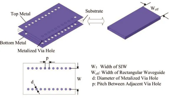
SIW is a kind of substrate integrated circuit (SIC) in which a metallized via array is arranged on a dielectric substrate with a metal layer on top and bottom to realize a wave guide structure similar to a metal waveguide function. By converting the non-planar waveguide structure into a planar form, it is advantageous to adopt a technology such as a printed circuit board process and a low-temperature co-fired ceramic process. The rectangular SIW structure is shown in Figure 1. Because the side walls of the SIW structure are not continuous metal but separated metallization vias, the surface currents along the waveguide axis on the sidewalls are cut off, and the SIW supports only TE mode propagation. In most cases, only the TEm0 mode exists because the thickness of the SIW is much smaller than its
width [1].
The design of the SIW structure needs to satisfyp≤2dandp < λ/4 to ensure that electromagnetic energy does not leak from the metallized via gaps, and no bandgap is generated within the operating band, wherepis the distance between two adjacent metallized vias anddthe diameter of the metalized via. In order to accurately map the SIW and a dielectric-filled metal waveguide, the two structures have the same frequency and dispersion characteristics, and the equivalent width of the rectangular waveguideWef f in Figure 1 is required in terms of size. The formula is:
Weff =W −1.08×
d2
p + 0.1×
d2
W (1)
whereW is the width of the SIW andWeff the width of its equivalent metal waveguide. After mapping,
the cutoff frequencies, working modes, and analysis and design methods of SIW can all directly use metal waveguides. A large number of microwave devices based on SIW structures have been proposed, such as couplers, power splitters, resonators, filters, and antennas. In addition, because the SIW are self-packaged structures, their major losses originate from the medium and metallic conductors rather than external radiation.
Received 4 May 2018, Accepted 7 September 2018, Scheduled 4 October 2018
* Corresponding author: Yong-Zhong Zhu ([email protected]).
Figure 1. SIW equivalent diagram.
Compared with microstrip filters, filters based on SIW resonators still occupy large circuit layouts. In order to obtain more compact and smaller SIW filters, many scholars have studied and implemented the SIW resonators themselves. The miniaturization and folding of the SIW resonator is a typical example of the miniaturization technology of substrate integrated waveguides. The SIW structure itself is a reference to a metal waveguide structure, and the folding cavity structure that is currently widely used in SIW is originally proposed in a waveguide resonator [2]. Subsequently, the concept of folding was introduced into the design of SIW filters. There are also FSIW filters designed by scholars using folded SIW resonators. In [3], a dual-mode single-band filter was designed based on the TE102 and
TE201 modes in the FSIW resonator. Based on the dual-mode FSIW resonator, a four-mode band-pass
filter was designed by coupling between two cavities. In [4], a two-cavity tunable SIW filter was designed by combining a double-folded SIW (DFSIW) resonator with a quarter-mode. In [5], using the DFSIW resonant cavity unit and LTCC process, a fourth-order cross-coupled SIW filter with a center frequency of 60 GHz is designed. Using a combination of electrical coupling and magnetic coupling, a transmission zero is generated on each side of the passband. In this design, through the gap on the upper surface of the folded SIW cavity, the open-faced microstrip line on the top surface performs the opposite-side coupling feeding, eliminating the need for a strip-to-microstrip connector design. In [5], using a DFSIW resonant cavity unit combined with LTCC process, a fourth-order cross-coupled SIW filter with a center frequency of 60 GHz was designed by using a combination of electrical coupling and magnetic coupling to generate transmission zero points on both sides of the passband. Refs. [6, 7] also presented fan-shaped and triangular FSIW folded cavity structures. Folding the SIW cavity can effectively reduce the circuit area occupied by the SIW cavity. In [8], The designed filter studies a SIW filter that combines a T-septum structure with LTCC technology. It is actually a type of folded SIW.The proposed filter with fourth-order T-septum resonators has two transmission zeros, which can be adjusted flexibly by controlling the coupling strength and manner. However, until now, the application of folding technology in SIW has used asymmetrical cavity folding methods. The concept of symmetric folded SIW has been proposed in [9] but has not been studied in depth.
2. MINIATURIZED SFSIW CAVITY ANALYSIS
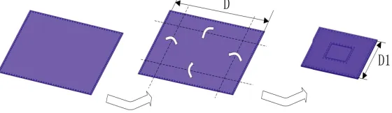
Figure 2 shows the evolution of the SFSIW resonator. Based on the original SIW resonator, the SFSIW is folded symmetrically to the center of the cavity parallel to the four sides. The folding process reduced the SFSIW cavity area to 27% of the original cavity size, but the cavity thickness was doubled.
Figure 2. Evolution process of SFSIW.
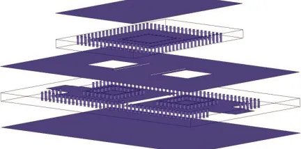
In Figure 3, the SFSIW resonator structure consists of three metal layers and two dielectric layers (Arlon AD260A, dielectric loss tangent 0.0017). The height of mediumh1 =h2 = 0.8 mm. The bottom and upper metal sheets, the middle and upper metal sheets are respectively connected through the metalized via. In order to achieve the effect of the folding, there is a gap between the middle metal layer and the metalized vias around the cavity, and the specific parameters of the cavity are shown in Table 1.
Figure 3. SFSIW resonator.
Table 1. Specific parameters of the SFSIW resonator (Unit: mm).
D L D1 D2 L2 L3 L4
38 20 19 8 18 17 7
There are three metal layers and two dielectric layers in the SFSIW resonant cavity. The resonant characteristics of the resonant cavity are determined by the electric field distribution when the cavity is in resonance. Figure 4(a) shows the electric field distribution in the upper metal layer of the resonator, and Figure 4(b) shows the electric field distribution in the middle metal layer of the resonator. It can be seen that the electric field in the intermediate metal layer is stronger than that in the upper metal layer.
(a) (b)
Figure 4. The energy distribution of metal layers.
7 8 9 10 11
3.7 3.8 3.9 4.0 4.1 4.2 4.3 4.4 4.5
D2 (mm)
f0 (GHz
)
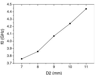
Figure 5. Relationship of SIW cavity size and resonant frequency.
(a) S11 (b) S21
2 4 6 8
-40 -30 -20 -10 0
f0 (GHz)
S11 (dB) SFSIW
SIW
2 4 6 8
-40 -30 -20 -10 0
f0 (GHz)
S21 (dB)
SIW
SFSIW
Figure 6. Comparison of transmission characteristics before and after folding.
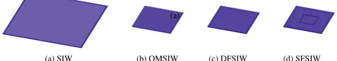
Schematic diagrams of different resonant cavities before and after folding are shown in Figure 7. In the SIW cavity miniaturization process, the degree of planar size reduction and Q value changes are shown in Table 2, and S0 and SSIW represent the surface size of the folded resonator and pre-folded
(a) SIW (b) QMSIW (c) DFSIW (a)
(d) SFSIW
Figure 7. Comparison of miniaturization.
Table 2. Specific parameters of the SFSIW resonator (Unit: mm).
SIW QMSIW DFSIW SFSIW
S0
SSIW 1 0.25 0.25 0.27
Q value 199 240 251 288
3. TWO CAVITY SFSIW FILTER DESIGN
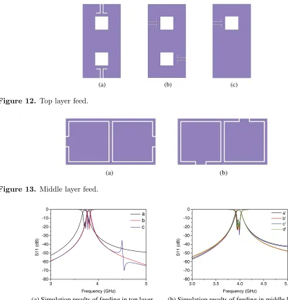
The coupling of the SFSIW cavity is realized by conventional open-window, and the coupling window is opened between two adjacent resonant cavities so that the two cavities work in the same mode to obtain the positive coupling. Coplanar waveguide and microstrip line are used for feeding, which are shown in Figure 8. Utilizing the feed structure of the upper or middle metal layer, the filter is matched to the source and the load to achieve the filter characteristics.
By comparing the upper coplanar waveguide feeding method and the middle layer microstrip line feeding method, the electric field distribution of the upper metal layer of the resonator and the electric
(a) (b)
Figure 8. Feed structure diagram.
(a) (b)
field distribution of the intermediate metal layer are shown in Figure 9. Using the method of microstrip feed in the middle metal layer, the electric field distribution in the cavity is stronger.
In the design of two-cavity filter structure, the characteristics of the SFSIW cavity folding make the two cavities have either the same direction or reverse directions in the cascade process. The structure of the SFSIW filter cavity is shown in Figure 10, where SFSIW cavities are cascaded in the same direction (In Figure 10(a)) and the opposite directions (In Figure 10(b)), respectively.
(a) (b)
Figure 10. Different cascaded SFSIW filter structure.
Figure 11. Parameters of filter.
Table 3. Parameters of filter size (Unit: mm).
D21 D22 D23 D24 P
19 38 3 5 1
a b c e i
4 1 4.5 2 0.25
(a) (b) (c)
Figure 12. Top layer feed.
(a) (b)
Figure 13. Middle layer feed.
(a) Simulation results of feeding in top layer (b) Simulation results of feeding in middle layer
3 4 5
-80 -70 -60 -50 -40 -30 -20 -10 0
a b c
Frequency (GHz)
S11 (dB)
3.0 3.5 4.0 4.5 5.0
-80 -70 -60 -50 -40 -30 -20 -10 0
a' b' c' d'
Frequency (GHz)
S11 (dB)
Figure 14. Different cascaded SFSIW filter structure.
In Figure 13, the feeding on the middle metal layer which uses a microstrip line structure also has two options, the horizontal feed and stagger feed. Due to the same and reverse directions cascaded between SFSIW cavities, there are four choices in the filter design process, namely the cavities are fed in the same direction horizontally or staggered, or the cavities are fed in the opposite directions horizontally or staggered, whose transmission characteristics correspond toa′,b′,c′,d′ in Figure 14(b), respectively. The center frequency (CF), bandwidth (BW) below−3 dB, insertion loss (S11) and return loss (S21) of the filter are shown in Table 4.
Table 4. Parameters of filter.
CF BW S11 S21
a 3.75 GHz 80 M −15 dB −1.1 dB
b 3.80 GHz 50 M −13 dB −1.6 dB
c 3.80 GHz 50 M −12 dB −1.7 dB
a′ 3.97 GHz 109 M −12 dB −0.99 dB
b′ 3.98 GHz 96 M −18 dB −0.92 dB
c′ 3.97 GHz 110 M −16 dB −0.80 dB
d′ 3.97 GHz 103 M −15 dB −0.90 dB
4. THREE CAVITY FILTER DESIGN
Using the SFSIW resonant cavity with the intermediate metal layer feeding method analyzed above, a three-cavity cross-coupled symmetric folded substrate integrated waveguide cross-coupling filter was designed as shown in Figure 15. The size parameters of each filter were determined by HFSS simulation.
Figure 15. Three-cavity SFSIW filter structure.
The three-cavity coupled SFSIW filter uses inductive and capacitive coupling to form a cross-coupling between the cavities. Coplanar cavities 1 and 2 are cascaded in the same direction, and a positive window is used to achieve positive coupling. As shown in Figure 16(c), the width of the inductive window D3 = 15 mm. The capacitive negative coupling between the cavities is achieved by means of narrow slits between the non-planar cavities 1, 3 and 2, 3 as shown in Figure 16(a). The cross-coupling matrix is:
0 0.136 0 0 0
0.136 0.011 0.124 0.044 0 0 0.124 −0.043 0.124 0 0 0.044 0.124 0.011 0.136
0 0 0 0.136 0
The structure of the cavity 3 is shown in Figure 16(b), and the parameters of the three-cavity cross-coupling filter are shown in Table 5.
5. FABRICATION AND MEASUREMENT
(a) (b)
(c)
Figure 16. Size parameters of three-cavity SFSIW filter.
Table 5. The size parameters of three-cavity SFSIW filter (Unit:mm).
L5 L6 L7 L8 L9 D3 D31 D32
49 30 7 20 30 15 38 19
D33 D41 D42 f g j k l
8 19 8 0.45 10 6.4 5.6 5.2
(a) (b)
2 3 4 5
-80 -70 -60 -50 -40 -30 -20 -10 0
Simulated S11 Simulated S21 Measured S21 Measured S11
Frequency (GHz)
S11 (dB)
-80 -70 -60 -50 -40 -30 -20 -10 0
S2
1 (dB)
Figure 17. Two-cavity miniaturized SFSIW filter.
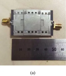
A three-cavity miniaturized cross-coupling SFSIW filter was produced as shown in Figure 18(a), which uses Arlon AD260A material. The height of the four layers medium is 0.8 mm, and the overall size of the filter is 49 mm×30 mm.
(a) (b)
2 3 4 5
-80 -70 -60 -50 -40 -30 -20 -10 0
Simulated S11 Simulated S21 Measured S21 Measured S11
Frequency (GHz)
S11 (dB)
-80 -70 -60 -50 -40 -30 -20 -10 0
S2
1 (dB)
Figure 18. Three-cavity miniaturized SFSIW filter.
Table 6. Comparison of different filters’ performance.
CF BW S11 S21 Size Reduction
This 3.98 GHz 100 M 25.5 dB −1.5 dB 73%
DFQMSIW in [4] 1.51 GHz 100 M −13.5 dB −1.9 dB 93%
T-Septum SIW in [8] 10.4 GHz 416 M 17.5 dB 2.52 dB *
DFSIW in [5] 62.7 GHz 6.7 G 13.6 dB 2.9 dB 74%
Figure 18(b) shows the comparison of simulated and measured results of this three-cavity cross-coupling SIW filter which works at 3.17 GHz with bandwidth of 320 MHz, insertion loss of −1.62 dB and return loss of −21.1 dB. The simulated and the measured results are also in good agreement.
6. CONCLUSION
In this paper, we propose a miniaturization method of symmetric folded substrate integrated waveguide resonator, which has a higher Q value and better transmission characteristics than the asymmetric folding of the SIW cavity. The degree of miniaturization and transmission characteristics of this structure are shown in Table 6. By analyzing different feeding and cavity cascade methods, a two-cavity and a three-two-cavity cross-coupling miniaturized SFSIW filter are designed. These filters have good transmission characteristics and achieve the miniaturization better, which make it valuable in applications such as satellite and other high quality communications systems.
ACKNOWLEDGMENT
REFERENCES
1. Chen, X. P. and K. Wu, “Substrate integrated waveguide filter: Basic design rules and fundamental structure features,”IEEE Microwave Magazine, Vol. 15, No. 5, 108–116, 2014.
2. Hong, J. S., “Compact folded-waveguide resonators,” Microwave Symposium Digest, 2004 IEEE MTT-S International. IEEE, Vol. 1, 213–216, 2004.
3. Zhang, R., Z. Wang, and B. Yan, “Dual-mode folded substrate integrated waveguide (FSIW) filters with LTCC technology,”International Conference on Microwave and Millimeter Wave Technology. IEEE, 1483–1485, 2010.
4. Zhou, J., Y. Z. Zhu, and Z. Liu, “A novel miniaturization double folded quarter mode substrate integrated waveguide filter design in LTCC,”Progress In Electromagnetics Research Letters, Vol. 60, 127–132, 2016.
5. Chien, H. Y., T. M. Shen, T. Y. Huang, et al., “Miniaturized bandpass filters with double-folded substrate integrated waveguide resonators in LTCC,”IEEE Transactions on Microwave Theory &
Techniques, Vol. 57, No. 7, 1774–1782, 2009.
6. Zhang, R., Z. Wang, B. Yan, et al., “FSIW cavity filter and derivative FSIW cavity and its filters with LTCC technology,” Microwave Conference, 2009. APMC 2009. Asia Pacific. IEEE, 1360– 1363, 2010.
7. Huang, T. Y., T. M. Shen, and R. B. Wu, “A miniaturized bandpass filter using quadruple folded laminated waveguide cavity resonators in LTCC,” Microwave Conference Proceedings. IEEE, 99– 102, 2011.
8. Tan, L., Z. Q. Xu, Z. Chen, et al., “A multilayer T-septum substrate integrated waveguide filter,”
Electromagnetics, Vol. 37, No. 4, 203–211, 2017.