Article
1
Effect of SLM Process Parameters on the Quality of
2
Al Alloy Parts; Part II: Microstructure and
3
Mechanical Properties
4
Ahmed H. Maamoun *1), Yi F. Xue1), Mohamed A. Elbestawi 1), Stephen C. Veldhuis1)
5
1)McMaster University, Department of Mechanical Engineering,1280 Main Street West Hamilton, ON,
6
Canada, L8S 4L7
7
* Correspondence: [email protected]; [email protected]
8
9
Abstract: Additive manufacturing (AM) provides customization of the microstructure and
10
mechanical properties of components. Selective laser melting (SLM) is the commonly used
11
technique for processing high strength Aluminum alloys. Selection of SLM process parameters
12
could control the microstructure of fabricated parts and their mechanical properties. However,
13
process parameter limits and defects inside the as-built parts present obstacles to customized part
14
production. This study is the second part of a comprehensive work that investigates the influence
15
of SLM process parameters on the quality of as-built Al6061 and AlSi10Mg parts. The microstructure
16
of both materials was characterized for different parts processed over a wide range of SLM process
17
parameters. The optimized SLM parameters were investigated to eliminate the internal
18
microstructure defects. Mechanical properties of the parts were illustrated by regression models
19
generated with design of experiment (DOE) analysis. The results reported in this study were
20
compared to previous studies, illustrating how the process parameters and powder characteristics
21
could affect the quality of produced parts. .
22
Keywords: Additive Manufacturing; Selective Laser Melting; AlSi10Mg; Al6061; SLM process
23
parameters; quality of the AM parts
24
25
1. Introduction
26
Industry 4.0 will open the way for a new age of advanced manufacturing. Additive
27
manufacturing (AM) is considered to be one of the leading sectors of the upcoming industrial
28
revolution [1]. AM of metals using selective laser melting (SLM), promises significant development
29
of a variety of critical applications in various industrial fields [2]. AM of Al alloys may produce
high-30
performance lightweight components with relatively high material quality, mechanical properties
31
and design flexibility. Selection of SLM process parameters plays an essential role in controlling the
32
material and mechanical properties of products customized according to their function and design
33
requirements. The effect of SLM process parameters on the quality of Al alloys was previously
34
presented in some studies [3–9]. However, the laser power of SLM was limited to 200 W due to its
35
limitations, a relatively low figure compared to the latest laser power which can reach 400 W. Fulcher
36
et al. [10] reported that the SLM process map should be regularly updated for each material as
37
technical capabilities develop. This could help to optimize the SLM process parameters and
38
customize the characteristics of the as-built parts. Consequently, the microstructure and mechanical
39
properties of the additively manufactured parts can be tailored according to their design
40
requirements. Akram et al. simulated a model of grain structure evolution in the multi-layer
41
deposition during the AM laser melting process [11]. Their results illustrated the change in grain size
42
and orientation according to select process parameters.
43
In SLM of Al alloys, the chemical composition of the Al alloys could cause variation between
44
their microstructure and mechanical properties, due to the difference in some elements such as Si and
45
Mg. However, SLM of some Al alloys, such as Al6061, results in solidification and liquation cracking
46
due to the material’s relatively higher coefficient of thermal expansion (CTE) [3]. This is why
47
AlSi10Mg is the most commonly used Al alloy for the SLM process due to its lower CTE compared
48
to the Al6061 alloy [10]. The Si content may also play a significant role in microstructure evolution
49
and elimination of hot cracks. Therefore, due to the widespread use of Al6061 in aerospace and
50
automotive fields, a study is recommended of the influence of SLM process parameters on this
51
material.
52
The current study focuses on the effect of SLM process parameters on microstructure and
53
mechanical properties of both AlSi10Mg and Al6061 as-built parts. This work completes the
54
comprehensive study presented in Part I to develop a full process map of different Al alloys
55
fabricated with SLM. The methodology of the design of experiment (DOE) is the same as in part I. A
56
regression model is created for each mechanical property according to the applied range of SLM
57
process parameters. The technique of one factor at a time (OFAT) is applied for AlSi10Mg parts, and
58
the response surface method is used for Al6061 parts. The regression model trend for each property
59
of the as-built parts is validated according to experimental results and additionally verified with
60
microstructure analysis.
61
2. Experimental procedure
62
In the current study, the samples were fabricated using SLM process parameters listed in Table
63
1, and Table 2, the same as used in part I. Similar experimental conditions were also applied as the
64
build plate was preheated to 200 ˚C, before building started under an argon medium. So,
65
AlSi10Mg_200C and Al6061_200C also referred to the as-built AlSi10Mg and Al6061samples
66
respectively. Microstructure analysis and the measurement of mechanical properties were performed
67
with the following methods.
68
2.1. Microstructure characterization
70
The microstructure of both AlSi10Mg and Al6061 as-built samples were characterized with
71
optical microscopy (OM), scanning electron microscope (SEM), and X-ray diffraction (XRD)
72
measurements. A Nikon optical microscope LV100 was used to evaluate the microstructure of the
73
etched parts. The polishing and etching procedures were performed according to the
74
recommendations of Maamoun et al. [12]. A TESCAN VP SEM, equipped with an energy dispersive
75
X-ray spectroscopy (EDS) detector, was used to investigate the grain size and structure observations.
76
A Bruker D8 DISCOVER XRD instrument provided with a cobalt sealed tube source was used for the
77
samples’ phase analysis. The XRD phase pattern was obtained for each sample along different
78
orientations of the AlSi10Mg and Al6061 samples.
79
2.2. Mechanical properties measurements
80
The microhardness measurement was performed according to ASTM E384-17 using an
81
automatic Clemex CMT tester. The average values of the samples’ microhardness were obtained
82
along the building direction (Z-direction), and along the plane parallel to the deposited layers
(XY-83
plane). Each recorded value was an average of 5-10 indentations along the tested area of a 200 gf load
84
applied over a 10 s dwell time. The residual stress was measured by an XRD instrument using a
85
Vantec500 area detector, and the results were analyzed using LEPTOS software. The tensile rod
86
samples were designed and fabricated according to the geometry and dimension included in ASTM
87
E8/E8M – 16a. The tensile test was performed according to ASTM E8 standard procedures using an
88
MTS Criterion 43 universal test system which applies a load capacity up to 50 kN.
89
3. Results and discussion
90
3.1. Microstructure
91
The optical microscope analysis was performed using the as-built etched samples of AlSi10Mg
92
and Al6061. Figure 1 shows the microstructure defects and observations along the building direction
93
(Z-direction) of AlSi10Mg samples fabricated at different SLM process parameters. Figure 1(a)
94
illustrates that process-induced porosity or keyhole pores of 100-250 µm size and irregular shapes
95
are formed inside the AS8 sample fabricated at a low energy density of 27 J/mm3. This results from a
96
lack of fusion due to insufficient powder delivery to the melted layer. Unmelted powder may be
97
visible around these keyhole pores [13]. Figure 1 (a) also shows that the melt pool solidified with an
98
elliptically shaped profile and these melt pool shapes overlap in a specific arrangement according to
99
the value of hatch spacing used. This shape is related to the Gaussian distribution of laser beam power
100
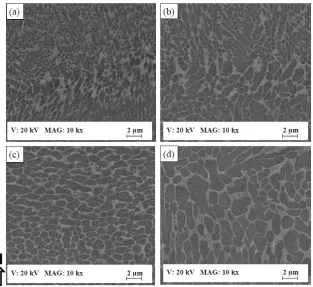
[12]. Figure 1(b) shows a magnified view of the melt pool shape; a fine grain structure is observed
101
inside, while a coarse grain is formed along its borders due to the gradient change of the solidification
102
rate. Figure 1(c) shows the microstructure of the AS7 sample fabricated at an energy density of 38
103
J/mm3. The keyhole pore density and size are decreased due to a higher energy density. The melt
104
pool shape geometry of the AS7 sample is enlarged compared to the AS8 sample due to a diminishing
105
solidification rate together with an energy density increase. In the AS3 sample produced at a 50 J/mm3
106
energy density, the keyhole pores almost disappeared as shown in Figure 1(d). A coarser grain
107
structure is also present inside and along the borders of the melt pool shape as illustrated in Figure
108
1(f). At a higher rate of energy density of 65 J/mm3 applied to the AS1 sample, melt pool borders
109
disappear along some layers and spherical hydrogen pores can be seen in Figure 1(e). The areas where
110
the melt pool borders disappear show a more homogeneous structure with elongated columnar
111
grains oriented along the building direction, Figure 1(g). While the areas displaying melt pool borders
112
show the same inhomogeneity of microstructure as in the other samples, they have a larger grain
113
structure as illustrated in Figure 1(h). It is worthwhile to note that the energy density level
114
significantly affects the solidification rate, and thus creates specific microstructure characteristics
115
corresponding to the applied values [14]. Also, according to the SLM process parameters listed in
116
Table 1 for each sample, the low laser power of 200 W applied to the AS8 sample results in low energy
density, and thus a lack of fusion according to the definition of the energy density in the following
118
equation:
119
𝐸 =
P
V ∗ 𝐷 ∗ T
(1)Where Ed represents energy density in J/mm3, P is the laser beam power (W), Vs is the laser scan speed
120
(mm/s), Dh is the hatch spacing between scan passes, Tl is the deposited layer thickness, which
121
remains a constant value in this study with a 30 µm height. The disappearance of the melt pool profile
122
borders observed inside the AS1 sample might be related to the reduction of the scan speed and hatch
123
spacing parameters.
124
125
SEM observations in Figure 2 and Figure 3 show the change in the developed microstructure
126
and the evolution of the Al matrix grain size of the as-built AlSi10Mg samples produced at different
energy densities and SLM process parameters. Figure 2 displays the microstructure along the
Z-128
direction of the AlSi10Mg samples. In general, the development mechanism of the as-built AlSi10Mg
129
microstructure depends on the mechanism of particle accumulated structure (PAS) formation [15].
130
The PAS mechanism shows that during the high cooling rate of 106-108˚C/s, Si is ejected out of the
131
solidifying Al matrix to form a fibrous Si network around the Al matrix grain borders. At a lower
132
energy density of 27 J/mm3, the microstructure shows an ultra-fine elongated grain structure with an
133
inhomogeneous size distribution of Al matrix grains surrounded by a fibrous Si network. The Al
134
matrix grain size ranges from 0.2 to 2 µm as displayed in Figure 2(a). The increase of energy density
135
to 50 J/mm3 results in the same microstructure formation with a coarser inhomogeneous
136
microstructure and grain size ranging from 500 nm to 3 µm. Figure 2 (c, d) shows that when the AS1
137
sample is produced at a higher energy density of 65 J/mm3, an equiaxed larger grain structure is
138
present with Al matrix grain size varying between 3-4 µm. A more homogeneous microstructure is
139
also obtained compared to the samples produced at a lower energy density. The final top layers in
140
Figure 2 (c) have a finer microstructure compared to the vicinity of the middle of the part in Figure
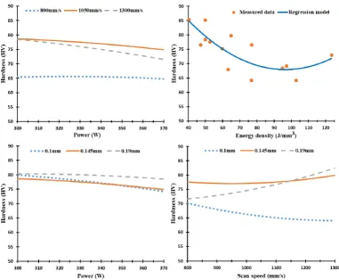
141
2(d). This is attributed to the thermal gradient difference between these areas during the building of
142
the layers, which affects the solidification rate.
143
145
The as-built AlSi10Mg samples along the XY plane had an equiaxed grain microstructure as can
146
be seen in Figure 3. The microstructure is inhomogeneous due to the existence of coarser grains along
147
the border of the melt pool profile compared to the microstructure inside. This confirms the PAS
148
formation mechanism of the microstructure development along the XY plane as well as the
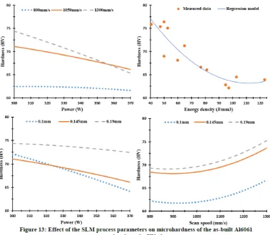
Z-149
direction. Figure 3 (a) shows the microstructure of the AS8 sample, where an inhomogeneous grain
150
distribution of 0.15-1 µm size can be seen within the fine and coarser Al matrix grain zone. The grain
151
size slightly increased along with energy density. Figure 3 (b) presents the microstructure of the AS3
152
sample with a grain size ranging from 0.3 to 2 µm. The microstructure evolution of the higher energy
153
density of 65 J/mm3 applied to the AS1 samples has almost the same Al matrix grain structure value
154
as illustrated in Figure 3(c). Application of energy densities higher than 50J/mm3 caused no significant
155
difference in the microstructure. However, the XRD measurements were performed for a more
156
accurate analysis of crystal size change and solubility percentage of the Si inside the Al matrix [16,17].
158
159
The XRD phase pattern presented in Figure 4 and Figure 5 shows a comparison of the Al and Si
160
peak characteristics of different AlSi10Mg samples. The Al and Si peak is identified using the Joint
161
Committee on Powder Diffraction Standards (JCPDS) patterns of 01-089-2837, 01-089-5012,
162
respectively. A small peak of Mg2Si is detected according to the JCPDS pattern of 00-001-1192, and
163
the low intensity of this peak is related to the existence of nano-size Mg2Si precipitates of 20-40 nm
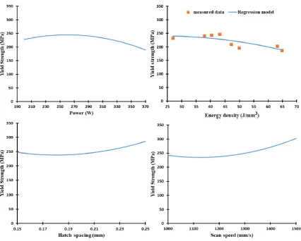
164
that are hardly detectable with XRD [12,17]. The difference in Al and Si peak width between the
165
samples indicates crystal size change under different SLM process parameters. This can be inferred
166
from Scherrer’s equation, where peak broadening varies inversely with crystallite size [18].
167
According to the phase pattern obtained in Figure 4, the grain size significantly increased along the
168
Z-direction as energy density increase to 50 J/mm3 before becoming stable at a specific value, which
169
agrees with microstructure observations in Figure 2. The XRD phase pattern in Figure 5 illustrates
170
the peak broadening comparison along the XY plane, where a slight difference of the crystal size is
171
observed between the samples fabricated at different SLM parameters. This corresponds to the SEM
172
observations in Figure 3. By comparing the peak broadening of the same sample along the Z-direction
173
and the XY plane, a significant difference can be seen in peak broadening and intensity. The
174
microstructure is inhomogeneous along different orientations. For more accurate values, an FWHM
175
analysis was performed according to the phase pattern in Table 3. The results showed a broadened
176
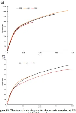
peak of Al and Si in the AS8 sample at the lower energy density, with FWHM values of 0.2111 and
0.5935 degrees respectively. This confirms the finer microstructure observed at the lower rates of
178
energy densities in Figure 2. The significant difference of Al and Si peak broadening in the AS8
179
sample along the XY plane and Z-direction also confirms the microstructure inhomogeneity at the
180
low energy of 27 J/mm3. There is no significant difference between the FWHM values detected along
181
the top and side orientations of the AS1 sample produced at a higher energy density of 65J/mm3. A
182
homogeneous equiaxed grain structure is present along the XY plane and Z-direction of the AS1
183
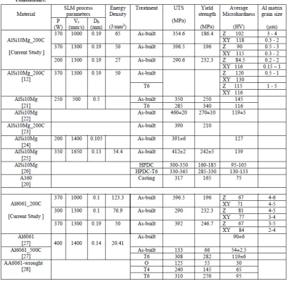
sample which indicates an improvement of the microstructure homogeneity at the higher energy
184
densities. A Rietveld analysis was performed to detect the relative weight percentage of Al and Si
185
according to the XRD phase pattern measured along the top and side surfaces of the AlSi10Mg
186
samples. The results listed in Table 4 indicate that Si becomes more soluble inside the Al matrix along
187
the XY plane as energy density gets higher. The percentage of Si solubility inside the Al matrix is
188
higher along the Z-direction compared to that in the XY plane for AS1 and AS3 samples after an
189
energy density of 27 and 50 J/mm3 is respectively applied. In addition, the highest percentage of Si
190
precipitates is obtained at the AS8 sample produced at the higher energy density of 65 J/mm3. These
191
results validate the thickness increase of the Si network at higher energy densities in Figure 2 and
192
Figure 3.
193
194
195
The microstructure of Al6061 samples shows hot crack formation in both the XY plane and
Z-196
direction as displayed in Figure 6. These cracks form as a result of solidification shrinkage and
197
thermal contraction, or liquation cracking inside the partially melted zone [3,19]. For the 6A sample,
198
hot cracks are observed along the XY plane within a size of 200-300 µm, and these cracks are
199
connected in a closed loop as illustrated in Figure 6 (a, c). The micro-cracks form into an elongated
200
shape within an average size of 200 µm along the Z-direction and propagate through the middle zone
201
of some solidified melt pool shape as shown in Figure 6 (b, d). A pore of 10-20 µm is also noticed
202
amongst these cracks. The micro-crack formation is caused by high CTE of the Al6061, which in turn,
203
resulted in significant shrinkage due to the rapid melting and solidification rates of the SLM process
204
[10]. A fine grain structure persists along both XY-plane and Z-direction as shown in Figure 6 (e, f).
205
Coarse grains are present around the melt pool profile, which substantiates the thermal gradient
206
inside each melt pool during the solidification process. It is worthwhile to note that no large keyhole
207
pores are observed inside the 6A sample microstructure fabricated with an energy density of 52.6
208
J/mm3. The evolution of crack formation behaves differently along the Z-direction, corresponding to
209
the applied energy density and SLM process parameters as shown in Figure 6 (b, g, h). Observations
210
indicate an increase of the crack size and distribution density under higher levels of energy densities
211
as illustrated in Figure 6 (g). Large hydrogen spherical pores were seen forming along the
212
longitudinal micro-cracks as energy density increased. By comparing the microstructure in Figure 6
213
(b, h), it can be concluded that a higher laser power and lower scan speed significantly increases the
length of the cracks and their distribution density due to the imbalance between the higher melting
215
and lower solidification rates.
216
217
The as-built Al6061 microstructure in Figure 7 shows the precipitation of nano-size Si particles
218
around the Al matrix grains, which confirms the PAS formation mechanism where the Si particles
219
solidified around the Al matrix. However, the same fibrous Si network is not present in the AlSi10Mg,
220
due to Si content in the Al6061 alloy being insufficient to develop this fibrous network. A fine
221
microstructure with an elongated grain form is observed along the Z-direction with a size of 3-5 µm
222
as shown in Figure 7 (a). Along the XY plane, an equiaxed grain structure is present, with an average
grain size of (2-4 µm), Figure 7 (b). The difference in the grain structure between these orientations
224
reveals a microstructure inhomogeneity which could result in anisotropic structure properties.
225
226
228
The XRD phase pattern in Figure 8 shows Al and Si peak up on the top surface of the as-built
229
Al6061 samples in the XY plane. Figure 9 illustrates the phase pattern up on the side surface along
230
the Z-direction. The Al peak is identified according to the JCPDS pattern of 01-089-2837. According
231
to the JCPDS patterns of 01-089-5012, a Si peak was hardly distinguishable due to the precipitation of
232
the nano-size Si particles inside the as-built microstructure as displayed in Figure 7. A low-intensity
233
peak of Mg2Si is also detected according to the JCPDS pattern of 00-001-1192 as indicated in Figure 8
234
and Figure 9. The change of Al peak broadening along the XY plane and Z-direction indicates Al
235
crystal size change according to the specified SLM process parameters. This change is closely
236
investigated using FWHM analysis listed in Table 5. A wider Al peak is obtained at a low energy
237
density of 50 J/mm3, which confirms the growth of the grain size as energy density increases.
238
According to Scherrer’s equation, the sharper peak in the XRD phase pattern indicates a larger crystal
239
size [18]. The FWHM shows a lower value of 0.1874 degrees in the 1A sample produced at an energy
240
density of 123.3 J/mm3, revealing a coarser grain structure at higher energy densities. There was no
241
significant difference between the FWHM values of the top and side surfaces. Al6061 microstructure
242
is more homogeneous along the applied range of the selected parameters as compared to the
243
considerable microstructure inhomogeneity inside AlSi10Mg samples. It is worthwhile to note that
244
the Al6061 alloy could be processed at higher energy density values than the AlSi10Mg alloy due to
245
the higher reflectivity of Al6061 which decreases the percentage of absorbed energy. However, SLM
246
process parameters need to be optimized to reduce the formation of micro-cracks and the spherical
247
hydrogen pores.
248
249
3.2. Mechanical properties
250
The effect of SLM process parameters on the mechanical properties of the as-built AlSi10Mg and
251
Al6061 parts is investigated according to the regression models developed from experimental results.
252
In the following section, DOE analysis will illustrate microhardness and tensile behaviour according
253
to the selected SLM process parameters.
3.2.1. Microhardness
256
Figure 10 displays the microhardness of the as-built AlSi10Mg parts along the Z-direction
257
within the range of SLM process parameters. The microhardness ranges between 86 and 103 HV, and
258
the maximum value is obtained at 27 J/mm3 due to smaller grain size. However, a significant amount
259
of keyhole pores are observed at this energy density of the AS8 sample, which underscores the need
260
for SLM process optimization. The results show that microhardness values linearly decrease as laser
261
power and energy density grow. A higher hatch spacing and scan speed improve sample
262
microhardness in Figure 10. Low values of sample microhardness at low scan speeds result from high
263
solidification rates and low hatch spacing due to decreasing overlap between the scanned passes. The
264
microhardness profile of AlSi10Mg samples shows a good agreement with microstructure
265
observations and the crystal size change of SLM process parameters.
266
267
As illustrated in Figure 11, microhardness along the XY plane is relatively higher than in the
Z-268
direction, demonstrating the inhomogeneity of the as-built microstructure. The microhardness is 115
269
to 118 HV along the range of the SLM parameters, which confirms better homogeneity along the XY
270
direction, Figure 3. This trend agrees with literature studies [12,14,16]. The reduction in laser power
271
and greater hatch spacing improves microhardness along the XY plane. Although the low laser power
272
rates show higher microhardness values, control of SLM process parameters should aim to produce
273
denser parts by reducing porosity. According to Figure 10 and Figure 11, microhardness values
274
correspond to the DOE analysis regression model along both the XY plane and Z-direction.
277
Figure 12 and Figure 13 display the microhardness profile of selected SLM process parameters
278
of the Al6061 parts along the XY plane and Z-direction. The map in Figure 12 shows a gradual
279
decrease of microhardness values along the Z-direction from 85 to 72 HV at an energy density range
280
of 40.5 to 97.2 J/mm3. A slight increase was observed at higher energy densities up to 123 J/mm3 as
281
illustrated in Figure 12. At a microhardness of 78 HV, a relation is observed between the low laser
282
power of 300 W and scan speeds of 1050 and 1300 mm/s. Scan speeds higher than 800 mm/s show a
283
significant increase in microhardness due to the associated higher rate of solidification. Results
284
indicate that a finer microstructure can be obtained at these higher scan speeds. Another interaction
285
between scan speed and hatch spacing occurs at a scan speed of 1050 mm/s and hatch spacing values
286
of 0.145 and 0.19 mm at a microhardness value of 77 HV as shown in Figure 12. The average
287
microhardness measure has a high scattering pattern around the regression model due to the effect
288
of the micro-cracks formed inside the parts.
290
Figure 13 shows microhardness of the Al6061 samples along the XY plane that varies
291
significantly between 62 to 77 HV according to the SLM process parameters. This could be related to
292
the change in micro-crack size as illustrated in Figure 6. In contrast with AlSi10Mg samples, hatch
293
spacing significantly affects the microhardness of Al6061. Microhardness gradually drops with the
294
increase of energy density.
295
Due to greater Si content, microhardness of AlSi10Mg samples was significantly higher than that
296
of Al6061 samples. The as-built AlSi10Mg samples have a higher microhardness than the same alloy
297
cast material, which is limited to 75 HV [20]. The particle size distribution of the powder and its shape
298
also might affect the microhardness of the as-built parts. This was demonstrated by comparing the
299
microhardness values in this study with those reported by Maamoun et al. at different powder
300
characteristics [12].
301
3.2.2. Tensile properties
302
The ultimate tensile strength (UTS) of the AlSi10Mg was measured to generate the regression
303
model plots for both as-built and machined tensile samples as presented in Figure 14. The as-built
304
and machined samples possessed the same tensile profile as the samples produced under SLM
305
process parameters. However, the machined samples had higher UTS values of up to 450 MPa
306
compared to those of the as-built samples (400 MPa). This 20 to 50 MPa difference in UTS values
307
indicates the effect of surface roughness on mechanical properties. However, UTS values of the
as-308
built parts could demonstrate the impact of SLM parameters on tensile properties, taking into
309
consideration the surface roughness of each sample. Figure 14 also shows a good agreement between
310
the experimental measurements and the regression model generated from the DOE analysis. Also,
311
laser power has a more significant effect on UTS sample properties than changes in hatch spacing
312
and scan speed. The optimum UTS value is obtained in the AS3 sample at an energy density of 50
313
J/mm3. This agrees with the microstructure observation, which showed minimum defects of the
as-314
built AlSi10Mg sample at these parameters.
317
Figure 15 illustrates yield strength versus the scan speed, laser power, hatch spacing, and the
318
energy density. Results indicate a decrease of yield strength within a range of 240 to190 MPa at
319
increasing energy densities. A slight difference of 30-50 MPa in yield strength was observed at the
320
range of SLM process parameters. This indicates that a change in SLM process parameters has a
321
greater impact on UTS values than the yield strength. UTS and yield strength trends significantly
322
reflect the microstructure observations in section 3.1. An increase of energy density creates a coarser
323
microstructure with lower hardness and tensile values.
326
As illustrated in Figure 16, the UTS values of the as-built Al6061 samples were investigated at a
327
range of 150 to 184 MPa. The results indicate a significant reduction in UTS of the Al6061 samples
328
compared to that of AlSi10Mg. This could result from the lower percentage of Si content inside the
329
Al6061 alloy and micro-cracks inside its as-built samples. As energy density increases, UTS values
330
gradually decrease. A maximum UTS of 184 MPa was obtained in the 18A sample using the higher
331
scan speed (1300 mm/s), hatch spacing (0.19 mm), and energy density of 47.2 J/mm3. A significant
332
decrease in the UTS values was observed at the lower scan speed of 800 mm/s and smaller hatch
333
spacing of 0.1 mm. This decrease in the UTS values might result from the microstructure defects at
334
low rates of scan speed and hatch spacing, such as keyhole pores or areas of unmelted powder. Yield
335
strength of the Al6061 samples is presented in Figure 17, where a similar trend as in UTS is present.
336
The yield strength values along the SLM parameters vary from 125 to 172 MPa. The maximum yield
337
strength of 172 MPa was detected in the 8A and 18A samples also produced at the higher scan speeds,
338
hatch spacing and energy density range of 40.5 - 47.2 J/mm3. It is worthwhile to note that the UTS
339
and yield strength values of the as-built Al6061 samples hardly differ, which indicates the lower
340
ductility of these parts compared to the as-built AlSi10Mg samples.
342
Figure 18 shows the stress-strain curve of the as-built samples for both AlSi10Mg and Al6061
343
alloys. Figure 18 (a) illustrates the stress-strain behaviour of the AS1, AS3, and AS8 AlSi10Mg
344
samples. The maximum UTS and highest ductility was observed in the AS3 sample produced at an
345
energy density of 50 J/mm3. Microstructure observations confirm that the optimum SLM process
346
parameters of the AlSi10Mg alloy are present in the AS3 sample. The AS1 sample was affected by
347
hydrogen pores and a coarse microstructure that forms at a higher 65 J/mm3 energy density, resulting
348
in lower stress value. Keyhole pores and lack of fusion negatively affected the quality of the AS8
349
sample produced at a low energy density of 27 J/mm3, which resulted in the lowest material strength
350
along with higher brittleness. The strain curve of the 1A, 4A, and 7A Al6061 samples is presented in
351
Figure 18 (b). Energy density change had no significant effect on the UTS value, whereas laser power
352
proved to be the most influential. The 4A sample produced at a low laser power level of 300 W,
353
exhibited minimum UTS values.
355
Table 6 summarizes the mechanical property values of the AlSi10Mg and Al6061 samples in the
356
current study, compared to literature. According to values listed in Table 6, the following insights
357
can be drawn:
358
1. Mechanical properties and Al matrix grain size are illustrated for the as-built AlSi10Mg_200C
359
samples in the current study. Although the lower rate of energy density created a fine microstructure,
360
mechanical properties were inferior due to the internal defects inside the areas caused by lack of
361
fusion.
362
2. The microhardness reported in a previous study by the authors [12], using the same
363
preheating technique, shows higher values than those reported in this study. This indicates the effect
364
of powder morphology and its particle size distribution. It can be concluded that a wide range of
365
particle size distribution with a spherical shape resulted in high microhardness values.
366
3. The mechanical properties of the AlSi10Mg_200C samples have relatively lower values than
367
those of samples produced by build plate preheating [21–25]. However, residual stresses are
368
significantly lower due to the preheating technique [4,12].
369
4. Superior mechanical properties of the AlSi10Mg_200C samples are detected compared to parts
370
produced with a conventional or the high-pressure die cast (HPDC) material of the same alloy [20,26].
371
5. As-built Al6061_200C parts had better mechanical properties than Al6061_500C. However, no
372
cracks were observed inside the Al6061_500C as reported by Uddin et al. [27], but the mechanical
373
properties of the part were significantly decreased.
6. The mechanical properties of the Al6061_200C samples show comparable values to the T6,
375
and T4 treated Al6061 wrought material [28].
376
4. Summary and conclusions
377
The current study focused on the influence of SLM process parameters on the microstructure
378
and mechanical properties of the as-built AlSi10Mg and Al6061 parts. The mechanical behaviour of
379
these parts along the range of selected SLM parameters was investigated using DOE regression
380
models. The main results are summarized as follows:
381
1. The microstructure of the AlSi10Mg parts changes significantly according to the applied
382
energy density. After solidification, the size of the melt pool profile increases together with energy
383
density. An energy density range of 50-60 J/mm3 was found to be the optimal range of the energy
384
density due to it minimizing keyholes and larger hydrogen spherical pores.
385
2. The grain size of the Al matrix inside the as-built AlSi10Mg samples grows along with energy
386
density. The microstructure homogeneity is also improved by the development of an equiaxed grain
387
structure at 65 J/mm3 along the Z-direction and XY plane. However, this can adversely affect the
388
relative density due to the formation of large hydrogen pores.
389
3. Micro-cracks form inside the microstructure of the as-built Al6061 samples. Size and
390
distribution of these cracks vary according to SLM process parameters. The smallest micro-cracks are
391
obtained at an energy density of 52.6 J/mm3 and a scan speed of 1000 mm/s.
392
4. The microstructure of Al6061 parts did not show the same fibrous Si network that formed
393
inside the AlSi10Mg microstructure due to lower Si content in the Al6061 alloy. The microstructure
394
of Al6061 parts followed the PAS mechanism, and nano-size Si particles precipitated along the grain
395
boundary of the AL matrix.
396
5. Microhardness of AlSi10Mg and Al6061 parts corresponds with microstructure observations
397
along the Z-direction and in the XY plane. However, Al6061 microhardness is affected by already
398
present micro-cracks.
399
6. UTS and yield strength of the as-built AlSi10Mg and the Al6061 samples are investigated
400
through regression models.
401
7. The effect of surface texture on UTS of the AlSi10Mg parts was investigated by comparing the
402
results from the as-built and machined tensile samples.
403
8. The mechanical properties of the studied Al alloys showed different values according to the
404
SLM process parameters, build plate temperature, powder characteristics, and the technique used in
405
Table 6.
406
The current work, together with part I, forms a comprehensive study of the SLM process
407
parameters effect on the quality of Al alloy parts. The results of this study could help customize the
408
properties of the parts according to design and function requirements. This work may also offer a
409
means to reduce post-processing treatment required for part characteristics in some applications.
410
Author Contributions: Formal analysis, Ahmed Maamoun and Yi Xue; Investigation, Ahmed Maamoun and Yi
411
Xue; Methodology, Ahmed Maamoun; Supervision, Mohamed Elbestawi and Stephen Veldhuis; Validation,
412
Ahmed Maamoun; Writing – original draft, Ahmed Maamoun and Yi Xue; Writing – review & editing, Ahmed
413
Maamoun, Mohamed Elbestawi and Stephen Veldhuis.
414
Acknowledgment: The authors would like to acknowledge the Additive Manufacturing Innovation Centre at
415
Mohawk College, Hamilton, Ontario, L9C 0E5, Canada and the XRD measurement analysis at McMaster
416
Analytical X-ray (MAX) diffraction facility.
417
References
418
1. Schwab, K. The Fourth Industrial Revolution; 2017;
419
2. Gibson, I.; Rosen, D.; Stucker, B. Development of Additive Manufacturing Technology. In Additive
420
Manufacturing Technologies; 2015; pp. 19–42 ISBN 978-1-4939-2112-6.
3. DebRoy, T.; Wei, H. L.; Zuback, J. S.; Mukherjee, T.; Elmer, J. W.; Milewski, J. O.; Beese, A. M.; Wilson-Heid,
422
A.; De, A.; Zhang, W. Additive manufacturing of metallic components – Process, structure and properties.
423
Prog. Mater. Sci. 2018, 92, 112–224.
424
4. Buchbinder, D.; Meiners, W.; Pirch, N.; Wissenbach, K.; Schrage, J. Investigation on reducing distortion by
425
preheating during manufacture of aluminum components using selective laser melting. J. Laser Appl.2014,
426
26, 012004, doi:10.2351/1.4828755.
427
5. Olakanmi, E. O. t; Cochrane, R. F.; Dalgarno, K. W. A review on selective laser sintering/melting (SLS/SLM)
428
of aluminium alloy powders: Processing, microstructure, and properties. Prog. Mater. Sci.2015, 74, 401–477.
429
6. Tradowsky, U.; White, J.; Ward, R. M.; Read, N.; Reimers, W.; Attallah, M. M. Selective laser melting of
430
AlSi10Mg: Influence of post-processing on the microstructural and tensile properties development. Mater.
431
Des.2016, 105, 212–222, doi:10.1016/j.matdes.2016.05.066.
432
7. Siddique, S.; Imran, M.; Wycisk, E.; Emmelmann, C.; Walther, F. Influence of process-induced
433
microstructure and imperfections on mechanical properties of AlSi12 processed by selective laser melting.
434
J. Mater. Process. Technol.2015, 221, 205–213, doi:10.1016/j.jmatprotec.2015.02.023.
435
8. Biffi, C. A.; Fiocchi, J.; Tuissi, A. Selective laser melting of AlSi10 Mg: Influence of process parameters on
436
Mg2Si precipitation and Si spheroidization. J. Alloys Compd. 2018, 755, 100–107,
437
doi:10.1016/j.jallcom.2018.04.298.
438
9. Krishnan, M.; Atzeni, E.; Canali, R.; Calignano, F.; Manfredi, D.; Ambrosio, E. P.; Iuliano, L. On the effect
439
of process parameters on properties of AlSi10Mg parts produced by DMLS. Rapid Prototyp. J.2014, 20, 449–
440
458, doi:10.1108/RPJ-03-2013-0028.
441
10. Fulcher, B. A.; Leigh, D. K.; Watt, T. J. Comparison of AlSi10Mg and Al 6061 Processed Through DMLS.
442
Proc. 25th Solid Free. Fabr. Symp.2014, 404–419.
443
11. Akram, J.; Chalavadi, P.; Pal, D.; Stucker, B. Understanding grain evolution in additive manufacturing
444
through modeling. Addit. Manuf.2018, 21, 255–268, doi:10.1016/j.addma.2018.03.021.
445
12. Maamoun, A. H.; Elbestawi, M.; Dosbaeva, G. K.; Veldhuis, S. C. Thermal Post-processing of AlSi10Mg
446
parts produced by Selective Laser Melting using recycled powder. Addit. Manuf. 2018, 21, 234–247,
447
doi:10.1016/j.addma.2018.03.014.
448
13. Sames, W. J.; List, F. A.; Pannala, S.; Dehoff, R. R.; Babu, S. S. The metallurgy and processing science of
449
metal additive manufacturing. Int. Mater. Rev. 2016, 61, 315–360.
450
14. Liu, Y. J.; Liu, Z.; Jiang, Y.; Wang, G. W.; Yang, Y.; Zhang, L. C. Gradient in microstructure and mechanical
451
property of selective laser melted AlSi10Mg. J. Alloys Compd. 2018, 735, 1414–1421,
452
doi:10.1016/j.jallcom.2017.11.020.
453
15. Prashanth, K. G.; Eckert, J. Formation of metastable cellular microstructures in selective laser melted alloys.
454
J. Alloys Compd.2017, 707, 27–34, doi:10.1016/j.jallcom.2016.12.209.
455
16. Maamoun, A. H.; Veldhuis, S. C.; Elbestawi, M. Friction stir processing of AlSi10Mg parts produced by
456
selective laser melting. J. Mater. Process. Technol.2019, 263, 308–320.
457
17. Maamoun, A.; Elbestawi, M.; Veldhuis, S. Influence of Shot Peening on AlSi10Mg Parts Fabricated by
458
Additive Manufacturing. J. Manuf. Mater. Process.2018, 2, 40, doi:10.3390/jmmp2030040.
459
18. Langford, J. I.; Wilson, A. J. C. Scherrer after sixty years: A survey and some new results in the
460
determination of crystallite size. J. Appl. Crystallogr.1978, 11, 102–113, doi:10.1107/S0021889878012844.
461
19. Carter, L. N.; Attallah, M. M.; Reed, R. C. Laser Powder Bed Fabrication of Nickel-Base Superalloys:
462
Influence of Parameters; Characterisation, Quantification and Mitigation of Cracking. In Superalloys 2012;
463
2012; pp. 577–586 ISBN 9780470943205.
464
20. Kaufman, J. G.; Rooy, E. L. Aluminum Alloy Castings: Properties , Processes , and Applications.; 2004; ISBN
465
0871708035.
466
21. Buchbinder, D.; Meiners, W. Generative fertigung von aluminiumbauteilen für die serienproduktion.
467
Fraunhofer Institute, Aachen, Ger.2010.
468
22. Kempen, K.; Thijs, L.; Van Humbeeck, J.; Kruth, J.-P. Mechanical Properties of AlSi10Mg Produced by
469
Selective Laser Melting. Phys. Procedia2012, 39, 439–446, doi:10.1016/j.phpro.2012.10.059.
470
23. EOS GmbH - Electro Optical Systems Material Data Sheet: EOS Aluminium AlSi10Mg; Munchen, 2014;
471
24. EOS GmbH - Electro Optical Systems Material Data Sheet: EOS Aluminium AlSi10Mg_200C; Munchen, 2013;
472
25. A.A, R.; M.S, W.; M., I.; K., K.; Ahmed, A.; S, S. Mechanical and Physical Properties of AlSi10Mg Processed
473
through Selective Laser Melting. Int. J. Eng. Technol. 2016, 8, 2612–2618,
474
doi:10.21817/ijet/2016/v8i6/160806217.
26. Lumley, R. N. Technical Data Sheets for Heat-Treated Aluminum High-Pressure Die Castings. Die Cast.
476
Eng.2008, 32.
477
27. Zia Uddin, S.; Espalin, D.; Mireles, J.; Morton, P.; Terrazas, C.; Collins, S.; Murr, L. E.; Wicker, R. Laser
478
powder bed fusion fabrication and characterization of crack- free aluminum alloy 6061 using in-process
479
powder bed induction heating. In Solid Freeform Fabrication Symposium; 2016; pp. 214–227.
480
28. Metals, A. S. for Metals handbook. 2. Properties and selection: nonferrous alloys and special-purpose
481
materials; American Society for Metals, 1990; ISBN 0871703785.