A Highly-Parallel Image Processing Computer Architecture Suitable
for Implementation in Nanotechnology
Cliristopher David Tomlinson
ProQuest Number: 10014706
All rights reserved
INFORMATION TO ALL USERS
The quality of this reproduction is dependent upon the quality of the copy submitted.
In the unlikely event that the author did not send a complete manuscript and there are missing pages, these will be noted. Also, if material had to be removed,
a note will indicate the deletion.
uest.
ProQuest 10014706
Published by ProQuest LLC(2016). Copyright of the Dissertation is held by the Author.
All rights reserved.
This work is protected against unauthorized copying under Title 17, United States Code. Microform Edition © ProQuest LLC.
ProQuest LLC
789 East Eisenhower Parkway P.O. Box 1346
Abstract
The anticipated properties o f future nanoelectronic devices represent orders o f magnitude
improvements in both packing density and switching speed over contemporary
microelectronic components. A potential use o f nanoelectronic devices is in the area o f
massively parallel computer architectures. At the forecast scale o f nanoelectronic devices,
a large processor array could be fabricated upon a single chip. This thesis examines issues
regarding the design o f such a nanoelectronic processor array.
A potential problem concerning the distribution o f control signals to processing elements
within a nanoelectronic array is discussed. A design for a novel massively parallel
architecture that overcomes the problem o f signal transmission along nano wires in such a
system is then presented. The proposed architecture, called the Propagated Instruction
Processor (PIP), requires only the local distribution o f control signals within the array. A
suitable processing element and instruction set for the PIP are defined and techniques for
programming the architecture are highlighted. Along with the architecture a methodology
for measuring the performance o f a massively parallel system is described, consisting o f an
architecture simulator and a set o f representative image processing operations. This test
set is implemented using simulations o f both the PIP and a more conventional SIMD
massively parallel architecture (CLIPS). The results o f the simulations allow a comparative
analysis o f the efficiency o f the PIP architecture to take place. Using the simulation results,
a number o f different architecture models are defined and are then used in the assessment
o f the PIP architecture. These are; a typical SIMD model, an all nanoelectronic SIMD
model, a nanoelectronic SIMD model with serial instruction word distribution and the PIP
model. The execution efficiency for these models, expressed in estimated clock cycles, on
the test set algorithms are then presented in full. Future areas o f investigation are indicated
Acknowledgements
I would like to express my gratitude to all o f my colleagues at the UCL Image Processing
Group for their help and patience throughout the last three and a half years. Special thanks
must go to Terry Fountain for his excellent supervision o f my work, strong support and
seamless management style. Dave Crawley has also been extremely helpful during my stay
here and I would like to express my thanks to him. Finally I would like to thank my wife
A Highly-Parallel Image Processing Computer Architecture Suitable for Implementation in Nanotechnology
Table o f C ontents
C h a p te r 1 Fast, P ortable, Parallel Computing
1.1 Introduction...1
1.2 Properties of Nanoelectronic Devices... 1
1.3 The Effective Use of Nanoelectronic Device Properties...3
1.4 Objectives of R esearch... 5
1.5 Research Methodology... 6
1.6 Sum m ary... 7
C h a p te r 2 Selecting a Parallel System for Nanoelectronic Im plem entation 2.1 Introduction... 8
2.2 SIMD Computing...8
2.3 The Processor A rrays... 10
2.3.1 The CLIP P ro g ra m ... 10
2.3.2 The CLIP3 Array Processor...11
2.3.3 The CLIP4 System ... 13
2.3.4 BASE4... 15
2.3.5 The Distributed Array Processor...17
2.3.6 The Connection M achine... 19
2.3.7 The AIS-5000...21
2.3.8 The Goodyear Massively Parallel Processor... 23
2.3.9 GEC Rectangular Image and D ata... 25
2.3.10 The Content Addressable Array Parallel Processor...27
2.3.11 The Associative String Processor... 28
2.4 Comparative Review...29
2.4.1 Interconnection Topology...30
2.4.2 Connectivity and Near Neighbour Parallelism ... 31
2.4.3 PE G ranularity...32
2.4.4 Long Distance Communication...33
2.4 Selection of a Starting Point for Further Research...34
2.4 Sum m ary... 34
C h ap ter 3 The Propagated Instruction Processor 3.1 Introduction... 36
3.2 Distributing Control - The Problem ... 36
3.3 Methods of Distributing Control to the P E s...37
3.3.1 A Hybrid SIMD System...38
3.3.2 A Buffered Nanoelectronic SIMD System...39
3.3.3 Propagated Instructions...40
3.4 Estimated Performance of tlie Proposed Systems...43
3.5 The Propagated Instruction Processor...44
3.5.1 Processing Element D esign... 44
3.5.2 Data Conditional Branching... 45
3.6 PIP Instruction S e t... 47
3.6.1 Array Instructions...48
3.6.2 Branch Instructions... 49
Chapter 4 A Fram ework for the Evaluation of a Parallel Architecture
4.1 Introduction... 53
4.2 Approach to Benchmarking...53
4.2.1 Selection of Test Suite... 54
4.2.2 The Test Suite... 55
4.3 Implementation D etails... 56
4.3.1 Algorithm Selection and Programming Style... 56
4.3.2 Image M apping... 56
4.3.3 Input and Output of D ata... 57
4.4 The Processor Array Simulation System (PASS)...57
4.4.1 Level of Simulation... 57
4.4.2 The Structure of P A S S ...58
4.4.3 Performance Assessment... 59
4.5 SIMD Array Programming Techniques... 60
4.5.1 Virtual Shifting... 60
4.5.2 Constructing a Ramp Im age...60
4.5.3 Column and Row Wise Operations...61
4.6 Definition of the Test S uite... 61
4.6.1 Point Operations...62
4.6.2 Local Neighbourhood Operations...65
4.6.3 Global O perations...68
4.6.4 Object Operations...76
4.7 Sum m ary... 78
Chapter 5 Program m ing the PIP Architecture 5.1 Introduction... 79
5.2 Types of Operation...79
5.2.1 Point Operations...79
5.2.2 Local Neighbourhood Operations... 80
5.2.3 Column Global Operations... 86
5.3 Programming Techniques... 87
5.3.1 Building a Ramp Image...87
5.3.2 Rowwise Arithmetic... 89
5.3.3 Rowwise Rotation...90
5.3.4 Repeated Row Wise Rotation...92
5.4 The Algorithms... 92
5.4.1 Point and Local Neighbourhood Algorithms... 93
5.4.2 Global Algoritlims...93
5.4.3 Object Algorithms...98
Chapter 6 Presentation and Analysis of Results for Point and Local Neighbourhood Operations
6.1 Introduction... 101
6.2 Point O perations...102
6.3 Local Neighbourhood Operations...108
6.5 Sum m ary...112
Chapter 7 Presentation and Analysis of Results and Analysis for Global Operations 7.1 Introduction... 114
7.2 Global Operations - an Overview... 115
7.2.1 The Hough Transform ...116
7.2.2 The ID Discrete Fourier transform... 117
7.2.3 Histogram m ing...118
7.2.4 Matrix Multiplication...121
7.2.5 R otation... 124
7.2.6 Magnification... 126
7.5 Conclusions... 129
Chapter 8 Presentation and Analysis of Results and Analysis for O bject Operations 8.1 Introduction...131
8.2 Skeletonisation...132
8.3 Adaptive Edge E xtraction... 135
8.4 Connected Component Labelling... 142
8.5 Object Operations - a Summary... 145
Chapter 9 Conclusions and Future W ork 9.1 Introduction...147
9.2 Designs for a Nanoelectronic Massively Parallel Architecture...147
9.3 Novel Programming Methods... 149
9.4 Performance Evaluation... 150
9.5 Future Work... 152
9.5.1 Processing Element Design...152
9.5.2 Array Control Unit D esign... 155
9.5.3 Overall Gating Structure... 155
9.5.4 Propagating Information and Object Operations...155
9.6 Concluding Rem arks... 156
R eferen ces...158
Appendix I Conditional Branch Instructions - A Possible Implementation Appendix II The CLIP3 Array Processor
A Highly-Parallel Image Processing Computer Architecture Suitable for Implementation in Nanotechnology
Table of C h arts
6.1 Microinstruction Cycles for the Logical AND Operation ... 104
6.2 Microinstruction Cycles for the Multiplication Operation... 104
6.3 Microinstruction Cycles for the Thresholding Operation... 104
6.4 Microinstruction Cycles for the FP Division Operation...104
6.5 Microinstruction Cycles for tlie Dilation Operation...110
6.6 Microinstruction Cycles for the Sobel O perator... 110
6.7 Microinstruction Cycles for the Median Filter Operation... 110
6.8 Instruction Type as a % of Overall Execution Time (Dilation)...110
6.9 Instruction Type as a % of Overall Execution Time (Median)...110
6.10 Instruction Type as a % of Overall Execution Time (Sobel)... I l l 6.11 PIP Algorithm Execution Cycles a % of SIMD Cycles (Point and LN )... 112
7.1 Microinstruction Cycles for tlie Hough Transform... 118
7.2 Microinstruction Cycles for the ID DFT...118
7.3 PIP Algorithm Execution Cycles a % of SIMD Cycles (Global)...129
8.1 PIP Algoritlim Execution Cycles a % of SIMD Cycles (Skeletonisation).145 8.2 PIP Algorithm Execution Cycles a % of SIMD Cycles (A EE)... 145
A Highly-Parallel Image Processing Computer Architecture Suitable for Implementation in Nanotechnology
Table of Figures
2.1 Illustration of an SIMD Architecture... 9
2.2 The CLIP3 P E ... 12
2.3 The CLIP4 P E ... 14
2.4 The BASE PE in Near-Neighbour Instruction M ode...16
2.5 The ICL DAP P E ...18
2.6 The Connection Machine P E ... 20
2.7 Functional Use of the AIS-5000...22
2.8 The MPP PE... 24
2.9 The GRID P E ... 26
2.10 The Associative Processing Element... 29
3.1 An SIMD System, On-Chip and Off-Chip Components... 37
3.2 A Hybrid SIMD System... 38
3.3 A Buffered SIMD System...39
3.4 The Concept of Propagating Instructions...41
3.5 The Concept of Task Pipelining... 42
3.6 The PEP Processing Element... 44
3.7 PIP Overall G ating...46
3.8 The PIP Instruction Word (Array)...48
3.9 The PIP Instruction Word (Branch)... 50
4.1 Processor Array Simulation System Overview...58
4.2 The PASS User Interface... 59
4.3 The Two Mask Planes used in the Matrix Multiplication Algoritlim... 70
4.4 The Nonnal Parameters for a Line... 72
4.5 The Eight Thinning Masks used in the Skeletonisation A lgorithm ... 76
5.1 The Eight Thinning Masks used in the Skeletonisation A lgorithm ... 85
5.2 An Illustration of Rowwise Rotation on a 4 x 4 ... 90
5.3 Repeated Rowwise Rotation on a 4x4 Array...92
5.4 Matrix Multiplication of a 3x3 Array (SIMD)... 94
5.5 Matrix Multiplication of a 3x3 Array (PIP)... 95
8.1 The 32^ Input Image to tlie AEE Algorithm... 136
8.2 The Modified PIP PE... 138
8.3 The 256^ Input Images to the AEE Algorithm ...140
A Highly-Parallel Image Processing Computer Architecture Suitable for Implementation in Nanotechnology
Table o f G rap h s
6.1 PIP Pipeline Latency as a % of Overall Execution Cycles ... 105
6.2 The Effect of Varying B for the Logical AND Operation...106
6.3 The Effect of Varying B for the Thresholding O peration...106
6.4 The Effect of Varying B for the Multiplication Operation... 107
6.5 The Effect of Varying B for the FP Division Operation...107
6.6 The Effect of Varying B for the Dilation O peration... I l l 6.7 The Effect of Varying B for the Sobel O perator... I l l 6.8 The Effect of Varying B for the Median Filter Operation... I l l 7.1 Microinstruction Cycles vs. Array Size for the Histogramming O peration... 120
7.2 Microinstruction Cycles vs. Array Size for the Histogramming Operation (SIM D )...120
7.3 Microinstruction Cycles vs. Array Size for the Histogramming Operation (P IP )... 120
7.4 Microinstruction Cycles vs. Array Size for tlie MM Operation...123
7.5 Microinstruction Cycles vs. Array Size for the MM Operation (SIMD)... 124
7.6 Microinstruction Cycles vs. Array Size for the MM Operation (PIP)...124
7.7 Microinstruction Cycles vs. Array Size for the Rotation O peration...125
7.8 Microinstruction Cycles vs. Array Size for tlie Rotation Operation (SIM D )... 126
7.9 Microinstruction Cycles vs. Array Size for the Rotation Operation (P IP )...126
7.10 Microinstruction Cycles vs. Array Size for the Magnification Operation...127
7.11 Microinstruction Cycles vs. Array Size for the Magnification Operation (SIMD)... 128
7.12 Microinstruction Cycles vs. Array Size for the Magnification Operation (PIP)... 128
8.1 Microinstruction Cycles vs. Array Size for the Skeletonisation Operation (M 0 D = 6 )... 133
8.2 Microinstruction Cycles vs. MOD for the Skeletonisation Operation... 134
8.3 Microinstruction Cycles vs. MOD for tlie Skeletonisation Operation (SIMD)... 135
8.4 Microinstruction Cycles vs. MOD for tlie Skeletonisation Operation (PIP)...135
8.5 Microinstruction Cycles vs. Array Size for the AEE Operation (MAPP=62) (1)... 137
8.6 Microinstruction Cycles vs. Array Size for tlie AEE Operation (MAPP=62) (2)... 139
8.7 Microinstruction Cycles vs. MAPP for tlie AEE Operation... 141
A Highly-Parallel Image Processing Computer Architecture Suitable for Implementation in Nanotechnology
Table of Tables
1.1 Forecast properties of CMOS and Nanoelectronic Devices... 2
1.2 Estimates of Array Packing Densities constructed of CMOS and NanoDevices... 5
2.1 CLIP3 System Statistics... 13
2.2 CLIP4 System Statistics... 15
2.3 BASE System Statistics... 17
2.4 DAP System Statistics... 19
2.5 CM-1 System Statistics...21
2.6 AIS-5000 System Statistics... 22
2.7 MPP System Statistics...24
2.8 GRID System Statistics... 26
2.9 CAAPP System Statistics... 27
2.10 ASP System Statistics... 28
2.11 Design features of Reviewed Systems... 29
3.1 Microinstruction Execution Time for a Single Instruction... 43
3.2 Task Execution Times for the Candidate D esigns... 43
3.3 The Instruction Mnemonics (Array Instructions)... 49
3.4 Some Typical Array Instructions... 49
3.5 Unconditional Branch Instruction Mnemonics...50
3.6 Branch and Continue Instruction Mnemonics...50
3.7 Branch and Wait Instruction Mnemonics...51
4.1 Operation Type vs. Data Type of the Test Suite ... 56
4.2 Exception Handling Implemented in the FP Division A lgorithm ...65
5.1 Data Transfer with Left Hand Column... 81
5.2 Data Transfer with Right Hand Colum n...83
5.3 Dilating a Binary Im age...84
5.4 Generating the Two Isbs of a Ramp Image... 88
5.5 Rowise Addition - Generating the Isb... 89
5.6 Operation Type vs. Data Type of the Test Suite O perations... 92
6.1 Microinstruction Cycles derived for Point Operations...103
6.2 Microinstruction Cycles derived for Local Neighbourhood Operations... 108
7.1 Simulated Array Size vs. Global O peration...114
7.2 Microinstruction Cycles derived for the Hough Transfonn...116
7.3 Microinstruction Cycles derived for the ID D F T ... 117
7.4 Microinstruction Cycles derived for the Histogramming Operation (1 ) ... 119
7.5 Microinstruction Cycles derived for the Histogramming Operation (2 ) ... 121
7.6 Microinstruction Cycles derived for the Matrix Mult. Operation... 122
7.7 Microinstruction Cycles derived for the Rotation Operation... 125
7.8 Microinstruction Cycles derived for the Magnification Operation... 128
8.1 Total Microinstruction Cycles derived for Skeletonisation on differing Array Sizes 132 8.2 Microinstruction Cycles for the Skeletonisation Operation (256^ Array)...134
8.3 Total Microinstructions derived for AEE on differing array sizes (1 )...136
8.4 Total Microinstructions derived for AEE on differing array sizes (2 )...139
8.5 Microinstruction Cycles derived for the AEE Operation (256^ A rray)... 142
Chapter 1 Fast, Portable, Parallel, Computing
1.1 Introduction
There is a fundamental limit on the continuing downsizing o f conventional
microelectronic components from which parallel systems are made, corresponding to
a minimum feature size o f approximately 50nm [1]. Beyond this limit, quantum
mechanical effects will start to interfere with the switching operation o f transistors,
leading to phenomena such as current leakage which render the device useless. One
area o f current research is investigating a potentially smaller class o f devices, called
nanoelectronic devices, in which device operation will depend upon the quantum
mechanical properties o f materials rather than be adversely affected by them. By
utilising quantum mechanical effects the downsizing o f components can continue to
the atomic scale. If research into nanoscale devices is fruitful then the available
packing density and clock speed o f future computer systems is likely to increase by
orders o f magnitude over contemporary standards. This thesis will examine designs
for parallel computer systems that could be composed from such nanoelectronic
devices.
Research into uses o f such nanoscale devices is still at an early stage and in the
absence o f any working devices at the nanometre sizes forecast, must be extremely
speculative. This work is no exception to this statement and much o f what is
contained herein is based on reasonable assumptions about what is currently known in
this developing field.
1.2 Properties of Nanoelectronic Devices
This thesis will not examine any particular nanoelectronic device in detail but will
briefly define a set o f generalised properties o f the devices that correspond to the
current forecasts for nanoelectronic devices. Surveys in which various nanodevices
are grouped into a number o f classes can be found in [1,3], with a more detailed
account contained in [2]. Although as a whole the different types o f nanoelectronic
devices can be recognised as a group - they all work because o f quantum mechanical
separate device groups are at different stages o f development, some exist only in
theory or simulation whilst others have been fabricated (although not necessarily at
the nanometre scale). Despite these difficulties, it is possible to set out some universal
characteristics that are widely forecast for all the groups o f nanoelectronic devices
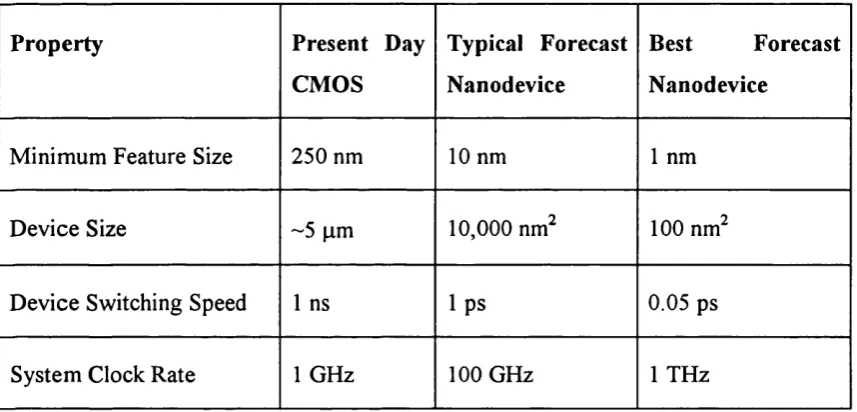
that have been identified. Some o f these estimates are shown in Table 1.1 along with
the equivalent properties for contemporary CMOS components. Two figures are given
for nanoelectronic devices, one that represents a typical forecast o f component size
and one that represents a lower limit on the size o f nanoelectronic components.
P ro p e rty P resen t Day
CM O S
Typical F orecast
N anodevice
Best F orecast
N anodevice
Minimum Feature Size 250 nm 10 nm 1 nm
D evice Size ~5 pm 10,000 nm^ 100 nm^
D evice Switching Speed 1 ns 1 ps 0.05 ps
System Clock Rate 1 GHz 100 GHz 1 THz
T ab le 1.1 Forecast P roperties o f C M O S and N anoelectronic devices
Along with the beneficial characteristics shown in table 1.1, it has also been widely
recognised that long distance communication between sites in nanoelectronic circuits
will be problematic [3], either because o f a transmission latency or signal degradation.
The recognition o f this problem has wide implications for designers o f systems to be
composed o f nanoelectronic devices. Indeed any system that is to benefit from the
potential advantages o f nanoelectronic systems must take this shortcoming into
account. To summarise this section, the important properties o f nanoelectronic
devices with regard to this thesis can be defined as follows;
• High Potential Packing Density
• Low Power
• Difficult long distance communication
1.3 The Effective Use o f Nanoelectronic Device Properties
A significant challenge for a system designer is to use the properties o f nanoelectronic
components in a productive and efficient way. The potentially high packing density
o f nanoelectronic components would allow for extremely complex systems to be
constructed in a very small area o f semiconductor. One area that has been suggested
by a number o f authors as a potential beneficiary from the properties o f
nanoelectronic devices is massively parallel processing (MPP) [4,5]. All
contemporary MPP systems suffer from the following shortcomings;
• The number o f processing elements (PEs) in the processor array is often smaller
than the data sets that the MPP has been designed to process. This limitation
necessitates the artificial partitioning o f data sets prior to processing, which in turn
leads to longer processing times.
• The size o f the on-chip memory for each PE is also limited by the lack o f
available packing density. This problem can be overcome by providing extra
memory off chip, however, a time penalty is incurred for off chip access.
• To maximise the number o f cells in the array, the PEs are often o f a simple single
bit design. Consequently seemingly ‘simple’ arithmetic operations may need tens
o r hundreds o f assembly language instructions for completion on an MPP. This
limitation leads to a constraint on the complexity o f tasks that can be executed in
real time.
• The large physical sizes o f the systems make the construction o f portable devices
that use MPPs unfeasible.
All o f the points above are related to the limitations imposed by the packing density
o f CMOS components available for the construction o f contemporary MPP systems.
current situation, table 1.2 contains some estimates as to the array sizes o f MPP
systems that could be constructed on Icm^ o f semiconductor in the different
technologies shown previously. These figures are based upon a set o f conservative
assumptions as follows:
• The array will be implemented on a single die o f lc m \ 50% o f which is given over
to external signal buffering
• The PEs o f the array are o f a simple single bit design and each requires 200
transistors
• Each PE also has 1Kbyte o f memory (dynamic RAM) consisting o f 20,000
transistors
• There are 35 control lines for each PE
• The minimum feature size o f the microelectronic components is 1pm. Two
different minimum feature sizes have been used in the calculations for the
nanoelectronic systems; Inm and lOnm.
• The width o f each control line for microelectronic technology is 250nm on 500nm
pitch. Calculations for the nanoelectronic systems are made at two different scales;
Inm on 2nm pitch and lOnm on 20nm pitch which correspond to the two different
minimum feature sizes.
Even with the set o f conservative assumptions made in the estimates o f Table 1.2 it
would appear that a nanoelectronic processor array could solve the problems o f
limited packing density highlighted earlier on in this section. Construction o f a
nanoelectronic array with devices o f minimum feature size lOnm would allow for a
500 X 500 PE array on Icm^ o f semiconductor. At the smallest potential device size
forecast, a Inm minimum feature size, a 5000 x 5000 PE array could be constructed in
the same area.
I f implemented, a processor array o f this size would allow very large data sets to be
processed without partitioning. Along with the increase in packing density, a large
increase in switching speeds when moving to nano scale devices is also forecast
[6,7,8]. It has been estimated that this would lead to an increase in processor array
clock speed o f at least 10"* over what is currently available (approx. 100 MHz) [9]. If
time applications than is currently possible. With the smaller physical array sizes, real
time applications that require highly portable computing facilities will also become
feasible [9]. In short, the advent o f nanoscale devices promises for the first time
massively parallel, high speed, portable computer structures.
P ro p erty CM O S ‘T ypical’
N anodevice
B est Forecast
Nanodevice
Devices / PE 200 200 200
Devices / PE
Memory
20,000 20,000 20,000
Area / PE (pm^) 1000 2 0.02
Area / PE Memory
(nm^)
100,000 200 2
Area / Control
Lines (pm^)
2,500 10 1
PE Units / cm^ 2 0 x 2 0 500 X 500 5000 X 5000
Table 1.2 E stim ates of A rray Packing Densities constructed of C M O S and
N anoelectronic Devices
1.4 O bjectives o f R esearch
Given the connection that has been shown between nanoelectronic devices and highly
parallel computing structures, the objectives o f this research can be defined as
follows;
1. To present suitable designs for a massively parallel computer architecture that
meet the anticipated constraint o f problematic long distance communication in
2. To devise, where it is necessary, novel methods for programming the architectures
defined.
3. To assess the viability o f the architecture designs by way o f a comparative study.
1.5 Research Methodology
The methodology used to meet the objectives defined in section 1.4 was as follows;
1. An existing SIMD architecture, CLIP3, was selected for use as a starting point in
the design o f the novel architecture. The selection procedure is contained in
chapter 2 o f this thesis, preceded by a review o f SIMD architectures.
2. A design for a novel highly parallel nanoelectronic architecture called the
Propagated Instruction processor (PIP) was developed using the existing SIMD
architecture chosen in chapter 2 as a base. The PIP and two other potential
nanoelectronic MPP architectures are described in chapter 3.
3. A representative test suite o f low level image processing algorithms that can be
used to assess the efficiency o f a highly parallel computer architecture was
selected and is presented in chapter 4. A series o f methods for programming the
PIP architecture were devised along with algorithms for implementing the test
suite. These are given in chapter 5.
4. The test suite algorithms were implemented on an assembly language instruction
level simulation o f the architecture to obtain a series o f performance figures in
terms o f instruction counts. The test suite algorithms were also implemented on
the other models o f parallel architectures so that a comparative study o f the results
could be achieved.
5. A comparative assessment o f the performance figures was carried out. As a result
o f the analysis modifications to the novel architecture were devised and
implemented with further experiments carried out on the modified system. This
process is described in chapters 6, 7 and 8.
6. A series o f conclusions drawn from the work are presented in the final chapter o f
1.6 Summary
The advent o f nanoscale components represents an opportunity for a large increase in
the numbers o f components that can be implemented on a single chip. This thesis
focuses on a class o f parallel computer system known as Massively Parallel
Processors (MPPs). There is a natural match between the (anticipated) properties o f
nanoelectronic devices and the architectural requirements o f MPPs [4,5]. Nanoscale
devices promise revolutionary increases in both device switching speeds and packing
density that will lead to very large, fast, portable computer systems. When designing
MPP systems comprising such nanoelectronic devices, the decisions confronting a
systems engineer are different from those affecting microscale design. This thesis
describes an investigation into one such design aspect o f a nanoelectronic MPP
Chapter 2 Selecting a Parallel System for Nanoelectronic Implementation
2.1 Introduction
The potential relevance o f nanoelectronic devices to the area o f massively parallel
computer architectures has been emphasised in the previous chapter. This chapter will
review a number o f massively parallel architectures, with the objective o f selecting a
particular architecture for use as a starting point in this research. The selected
architecture will be used later in the thesis as a first reference point when looking into
nanoelectronic designs for a massively parallel computer.
The chapter is set out as follows; First a description o f Single Instruction Multiple
Data (SIMD) computing is given, then a number o f existing massively parallel
systems are reviewed and finally a comparative analysis o f the existing systems is
presented. The comparative analysis will conclude by selecting one o f the reviewed
systems as a starting point for further research into nanoelectronic massively parallel
architectures.
The review will not attempt to rank the included designs. Indeed, as shown previously
by several authors, such a straightforward comparison is not usually valid in this field
o f highly specialised machines [10,11,12]. However some o f the performance figures
o f each machine will be listed here, in particular the statistics for some low-level
image processing operations (where they have been published). It is anticipated that
the use o f some nanoelectronic components in an identical system could improve
these figures substantially.
2.2 SIMD Computing
The control o f massively parallel systems is often achieved in an SIMD fashion, a
typical SIMD arrangement being shown in figure 2.1. It is usual for such a system to
consist o f a host computer, an array control unit (ACU), a processor array and an
array input/output arrangement. The processor array usually contains many thousands
o f identical processing elements (PEs). The PEs are often o f extremely simple design
and contain little or no independent program control hardware. Each PE contains
some exclusive local memory in which to store intermediate results. The PEs can also
transmit and receive data to and from other directly connected PEs by way o f an
interconnection topology. Figure 2.1 shows a four way connected mesh topology. The
broadcast the same instruction to all the PEs which can then operate on data items
local to each.
Processing Element
Control Distribution Lines
Data I/o Lines
HOST ARRAY
CONTROL UNIT (ACU)
DATA I/O INTERFACE
Figure 2.1 Illustration of an SIMD Architecture
SIMD systems are extremely suitable for massively parallel implementations that may
contain hundreds o f thousands o f PEs, because o f the simplicity o f programming the
structure. The operations performed on the PEs in an SIMD architecture are data
parallel, but the controlling program is sequential in nature. Various uses can be found
for SIMD systems, a suitable application area usually contains a large data set o f input
items each with the same (or similar) processing requirements. The data items are
distributed to the processor array prior to being processed by all PEs in parallel.
Suitable areas for massive parallelism include;
• Image Processing
• Scientific Computing (e.g. Finite Element Analysis)
• Data Base Manipulation
The chosen application area o f this study is image processing. Many o f the operations
in the early stages o f processing, for instance filtering and segmentation, involve
known as iconic in that they transform an N x N input image into an N x N output
image. In many procedures it is usual for a number o f iconic operations to be applied
in series to an image. In such a scenario, massively parallel processing becomes
attractive because o f the repetitive nature o f the task that must be applied to a very
large number o f data items (typically the image pixels). A mesh connected parallel
architecture is especially suitable for image processing as its topology directly
matches the input and output data structures required. If, however, the number o f PEs
in a massively parallel system is less than the number o f data items to be processed
then the performance o f an MPP will degrade significantly. All contemporary MPPs
have fewer PEs than there are pixels in standard image sizes [13,14,15]. This problem
could be overcome by utilising the very large increases in packing density that
nanoelectronic devices promise.
An appropriate starting point in MPP history for the review o f individual SIMD
systems that follows is the second generation o f processor array designs [16] where
the individual PEs were in the main single bit processors. The survey will continue
from this point to the present day where the advance o f technology and the lower cost
o f components have allowed processor arrays to become commercially viable.
2.3 The Processor Arrays
2.3.1 The CLIP Programme
The Cellular Logic Image Processing (CLIP) programme was initiated at University
College London after a system called U C PR l, comprising a 20 x 20 array o f fixed
logic elements proved successful in approximating areas o f interest in charged particle
tracks [17]. The first o f the CLIP processor arrays, C L IPl, was a prototype system
consisting o f a 100 processor element array (10 x 10), each element being connected
to its four orthogonal neighbours. The CLIPl PE was o f a very simple, bit-serial,
design and allowed only three basic operations on binary images; extraction o f the
contents o f closed loops, extraction o f segments attached to the array border and
extraction o f the outer edges o f segments. Subsequently, a programmable system
dubbed CLIP2, a 16 x 12 array with a hexagonal connectivity pattern, was developed.
Each CLIP2 PE consisted o f two Boolean processors each capable o f the sixteen
possible Boolean functions o f its two inputs. Both processors accepted the same two
inputs that could be either two binary images or one binary image and the result o f a
logical OR o f the PE's six neighbour connections. The output from one o f the Boolean
processors was designated as a signal for transmission to the six connected
neighbours, while the other, the processed binary image, was stored in local PE
memory. The major drawback with this design was that there was no way o f including
directional information in instructions as each o f the six signals from the connected
neighbours were all always included in the relevant instructions. With this in mind the
next o f the CLIP series, CLIP3, was designed and implemented to include
programmable interconnection directions. CLIP3 is described in detail in section
2.3.2.. Beyond CLIP3, the programme continued and a fourth prototype CLIP4 [18]
was developed. CLIP4 consisted o f a 96 x 96 mesh o f bit serial PEs and is described
in section 2.3.3. A later model in the CLIP series, the CLIP?A [19,20] prototype,
moved away from the original cellular logic concept and comprised a linear array o f
16 bit PEs.
2.3.2 The CLIPS Array Processor
The CLIP3 system, a working prototype, was completed in 1974 and included a 16 x
12 mesh connected array o f single bit PEs built out o f TTL components. The system
contained the usual elements o f an SIMD processor array; an array control unit
(ACU), an I / O arrangement, host computer and processor array.
The primary use o f CLIP3 was for binary image processing [21,22]. The system
allowed for two distinct neighbourhood connectivity patterns between the individual
PEs, square (eight connected) or hexagonal (six connected). Input o f an image to the
array was achieved by serially feeding the thresholded output o f a flying spot scanner
into a shift register - each bit o f which represented the A register in a particular PE.
Processing Element
A block diagram o f the CLIP3 PE is shown in figure 2.2. The function o f the PE can
be split into the following three areas;
• Neighbourhood input gating and the sum and threshold modules
• Registers and local memory
Image I/O
D Function Control ( C l..0 4 ) Neighbour
Selection (G1..G8)
Threshold Selection (F1..F3)
VV'M'
Memory Output
I M f U l f
Neighbour Input Z Z
(N 1 ..N 8 )=
Neighbour Output N Function
Control (C5..C8) Input
Gating
16 Bit RAM
Boolean Processor
Figure 2.2 The CLIPS PE
Neighbourhood Input Gating
Data is transmitted from other directly connected cells to the PE via the
neighbourhood inputs (N1-N8). Selecting the relevant control lines (G1-G8) acts as a
filter on the arriving signals. The use o f one line per neighbour permits any
combination o f these inputs to a PE. A summation circuit adds the number o f active
neighbour inputs and the result o f this is passed to the threshold module. The
threshold module produces a comparison between the number o f active inputs and a
user selected threshold (F1-F3). A signal is produced at T only if this threshold is
exceeded. The inclusion o f the summation and thresholding structures, although not
strictly necessary (it was not included in later CLIP machines), allowed certain useful
neighbourhood operations to be implemented in a single instruction step.
Registers and Local Memory
Each CLIPS PE contains the two single bit registers (A and B) and sixteen bits o f
local RAM. Prior to processing by the Boolean function generator, the appropriate
bits are loaded from local memory into the two single bit registers. When the value o f
the B register is passed to the Boolean function generator it is logically O R ’ed with
the output from the threshold gate. To perform operations involving the local
neighbourhood not involving B, it can be set to zero prior to the appropriate
instruction.
The Boolean Function Generator
The Boolean processor allows any o f the sixteen possible logical combinations o f its
two inputs to be selected for each o f its outputs. The functions are programmed by the
enabling o f combinations o f its control lines (C1-C8), four for each o f the outputs.
One output (N) provides the neighbour input for each o f the eight connected PEs, the
other provides the input to local memory (D).
CLIPS System Detail Performance - Basic operations.
Year : 1974 Data I/O time : 192ps
Developer ; UCL Integer Addition 50 ps (8 bits)
Status ; Experimental Integer Multiplication 1040ps (8 bits).
Topology : 6 or 8 Mesh FLOPS : N/A.
PE: Bit Serial Comparison operation : Ips
Array Size : 16x 12 Binary Pointwise Ips
Local Memory : 16 bits
Control Lines : 28 Local Neighbourhood operations Long Range Com: Global Propagation Binary Near neighbour Ips
Convolution (3x3 8 bits) 9760ps Binary Erode / Dilate 1 ps Data Shift: (8 bits) 8ps
Table 2.1 CLIP3 System Statistics
2.3.3 The CLIP4 System
The proposal for the CLIP4 program was generated in 1974 but a working
implementation was not in place until 1980 because o f difficulties in chip
procurement [23]. The system included an increased array size over CLIPS o f 96 x 96
PEs built from 0.168 x 0.177 inch customised integrated circuit chips, each CLIP4
chip containing eight processing elements and 256 bits o f RAM. Twelve o f these
chips were fitted to each array processor card with the overall array constituting 96 o f
these cards. All processing elements in the array operate in SIMD mode by executing
Processing Element
The design o f the CLIP3 PE was used as the base design for CLIP4 and many
similarities exist between the two. Again a two input / two output Boolean processor
formed the heart o f each processing element with the A register and neighbour input
values providing the input, the processed data and neighbour output values forming
the output. The analogue neighbour input summation and thresholding o f CLIPS was
scrapped in CLIP4, to implement this feature in digital logic would have doubled the
number o f gates needed to construct each PE. As in CLIPS, each neighbour input is
controlled by a single control line (G1-G8). The eight resulting signals are then
combined by an OR gate to produce a signal at T. A full adder with a circulated carry
bit was incorporated to improve the efficiency o f the arithmetic processing needed to
process grey scale images. The size o f local memory available was doubled from 16
to 32 bits although this still imposed limiting size restrictions upon the user
particularly when performing operations on grey scale images.
Enable B
Memory Output 32 Bit RAM
Image I/O
D Function Control ( C l..04) Neighbour
Selection
(G I..G 8) ^'V
uu
Neighbour Input == (N 1..N 8)=
Boolean Processor Input
Gating iiii
N Function Control (C5..C8)
Neighbour Output L oadD
Figure 2.3 The CLIP4 PE
When the R line is disabled the P input is, as in CLIPS, a logical OR o f the B register
and the neighbour signal (T) and the array can be used for the normal binary image
operations. When the R line is enabled the two NOR gates and an AND gate, act as a
half adder on the B and T inputs. The Boolean Processor can then be configured as a
second half adder to combine the output from these gates with the A register. The
result o f the addition o f two bit planes (A and B) is formed at D with the carry bit
being stored in the C register for re-circulation in the next addition cycle.
Alternatively addition can be carried out in a bit column fashion (i.e. each bit o f a
number is stored along a column o f P E ’s) where the T input is formed by allowing the
appropriate neighbour’s control line and the carry bit flows to the appropriate
neighbour.
CL1P4 System Detail Performance - Basic operations.
Year 1980 (designed in 1974) Integer Addition (8 bits) 80ps
Developer UCL Integer Multiplication (8 bits) 2000ps
Status Experimental FLOPS N/A.
Topology 6 or 8 Mesh Binary Pointwise lOjis
PE: Bit Serial
Array Size 9 6 x 9 6 Local Neighbourhood operations
Clock Rate 2.5 MHz Binary Near neighbour lOps
Local Memory 32 bits Averaging (3x3 8 bits) 1300ps
Control Lines 28 Median Filter (3x3 8 bits) lOOOOps
Long Range Com Global Propagation Convolution (3x3 8 bits) 18640ps Binary Erode / Dilate 10 ps Data Shift: (8 bits) 80ps
Table 2.2 CLIP4 System Statistics
2.3.4 BASE4
The BASE4 processor is a 4 x 4 prototype mesh processor that was constructed in
1980 at Purdue University under the direction o f Anthony Reeves [9] who had
previously worked in U CL’s Image Processing Group. In his description o f the system
it is mentioned that an 8x8 mesh (BASE8) was under construction and that larger
arrays o f this design had been simulated. The design o f the BASE processor closely
resembles that o f the two CLIP processors described previously. Reeves concedes this
in his description but adds that BASE has been ‘systematically’ designed, resulting in
a simply expressed instruction set whereas the CLIP series was a ‘sequence o f
hardware models each model being used as the basis for the next’. Reeves argues that
this simply expressed instruction set provides a sound base for the development o f a
higher level language. The other major differences between this design and the basic
CLIP processing element is a three input two output Boolean processor and the
manner o f operations that can be applied to the near neighbour inputs. CLIP3 includes
the useful analogue summation and threshold feature and in the CLIP4 system the
gating and also provides facilities for the combination o f input signals with the AND
function. A combination o f both logical relationships can be used to allow any single
bit pattern o f the eight near neighbours to be tested for.
Figure 2.4 The BASE PE in Near-Neighbour Instruction Mode
A three-input Boolean processor allowing any Boolean combination o f its three inputs
forms the hub o f the BASE system. The BASE processor allows for both local and
global propagation instructions (called recursive instructions by Reeves). The above
diagram shows the BASE processor in local propagating instruction mode - the near
neighbour output would have to be calculated in a prior instruction and stored in the B
register. For global propagation instructions the neighbour output is provided by the
R register.
BASE4 System Detail
Year 1980
Developer Purdue University
Status Prototype (Larger Arrays Simulated)
Topology 8 Mesh
PE: Bit Serial
Array Size 4 x 4
Control Lines 22
Long Range Com Global Propagation
Table 2.3 BASE System Statistics
2.3.5 The Distributed Array Processor (DAP)
The DAP is a processor array with mesh connections to orthogonal neighbours and
high speed data communication facilities. The DAP was first developed for scientific
computing at ICL principally by Reddaway, Hunt and Parkinson [24,25]. When the
first 32 X 32 prototype appeared in 1976 it became apparent that the DAP design was
versatile enough for it to be used in other areas including Image Processing. Later
updated versions o f the basic DAP design principles have been produced
commercially by Active Memory Technology (AMT) and more recently by
Cambridge Parallel Processing who acquired AMT in July 1992.
The ICL DAP
One o f the DAP systems to be developed commercially was the ICL DAP (1980) and
was a 64 X 64 mesh o f processing elements o f the type shown in figure 2.5. The single
bit PE consisted o f three registers (Q, C and A), input and output multiplexers, 4096
bits o f local memory and a one bit wide adder. The Q register can be considered as an
accumulator, the C register a carry bit and the A register can be used to implement
some local activity control. The neighbour input may also be written directly into the
A register or logically AND’ed with its contents. The DAP does not allow neighbour
input parallelism as in the CLIP series and the current neighbour input direction is
selected by the input multiplexer. In addition to the North, South, East and West
neighbour connections, each processor is connected to two data highways which span
each column and row o f the array. These allow data to be broadcast across the entire
array from the M CU in one cycle in either o f the two orthogonal directions. The
output multiplexer selects the PE output which may be; local memory, adder sum, the
Q register or the A register. A conditional write to memory can be achieved with the
A register acting as a control to the output multiplexer.
Although a full adder forms the heart o f this system it is possible to implement other
operations using this arrangement, for instance;
To load Q from memory the Q and C inputs to the adder are disabled.
To transfer Q to C the input from neighbour input is made true and the C input is
disabled. The array could be programmed by using the specially developed assembly
language APAL or by using the higher level FORTRAN Plus - a parallel extension o f
and gate
AD DER
row select
responses to MCU
to neighbours from neighbours
column data/ column select
memory 4k bits output multiplexer sum carry
input multiplexer
Figure 2.5 The ICL DAP PE
The AM T DAP 500/600 series
A later incarnation o f the DAP was called the AMT DAP which embodies the main
design principles o f the ICL DAP and is also workstation compatible [26]. The
500/600 series is commercially available and has been used on a number o f problems
such as; text searching, database operations, image processing and computational
fluid dynamics. The processing element design is very similar to that o f the earlier
model, the only differences being the provision o f two more single bit registers, S and
D [16], both o f which are shielded from the APAL programmers view. The D register
is used for fast I / O and can overlap processing with the rest o f the PE. Some o f the
single instructions provided on the DAP read from and write to memory and in order
to facilitate these the S register is placed in the data flow.
DAP System Detail Performance - Basic Derations.
Year 1989 Data I/O time I cycle (overlaps processing)
Developer AMT Integer Addition 2.5ps (8 bits)
Status Commercial System Integer Multiplication 16.3 ps (8 bits). Topology Mesh, 4 connected FP Addition/ 85.5ps (32 bits).
PE: Bit Serial FP Multiplication I70.6ps (32 bits).
Array Size 64 X 64 Binary Pointwise O.I ps (max).
Clock Rate 10 MHz
Local Memory 1 Mbit (max)
Long Range Com Orthogonal Data Buses
Table 2.4 DAP System Statistics
2.3.6 The Connection Machine
The Connection Machine was initially conceived by Daniel Hillis and others at MIT
as a way o f directly matching a computer architecture to the data structures involved
in solving an arbitrary problem [27]. To achieve this aim the Connection Machine
employed a flexible inter-processor communication structure. The first model, CM-1,
was designed originally for solving symbolic problems and consequently could be
programmed using a version o f Lisp (CM-Lisp). Later designs o f the connection
machine (CM-2 and CM-5) also had parallel versions o f imperative languages
available.
The Connection M achine 1 (CM-1)
The CM-1 consisted o f 4096 VLSI processor chips each housing 16 single bit PEs
arranged in a 4 connected mesh and a message router which occupies a significant
proportion o f each chip. The CM chips were connected in a Boolean «-cube topology
where the maximum possible distance between any two nodes o f the network is the
number o f dimensions, which in the case of CM-1 is twelve.
Processing Element
The single bit PE is o f relatively simple design, the basic operation being to combine
two bits contained in memory (defined by the A and B addresses) and a flag (defined
by the read flag) with a Boolean function (defined in the truth table) to produce two
outputs. One output is written back to the A memory address, the other to one o f the
flags defined by the write flag. The ALU is capable o f any o f the possible 65,536
possible Boolean functions containing three inputs and two outputs - these are
There are sixteen flags associated with each processor - eight o f these are for general
purpose use and the other eight for use by the system hardware such as a context flag
which dictates whether to execute conditional operations. Another o f these hardware
flags, the daisy chain flag, allows the sixteen cells upon a chip to be chained together
to perform sixteen bit operations.
ALU
flags b address
to router a address
read flag
truth table
write flag
4K memory
Figure 2.6 The Connection Machine PE
Communications
The on-chip router handles incoming and outgoing messages for the sixteen local
processing elements. The routers are connected by 24,576 bi-directional connections
forming a communications network in the pattern o f the n-cube. Messages are
addressed relatively with each dimension o f the hypercube making up one bit position
o f a twelve bit address. When a router receives a message its address is checked - if
this is twelve zeros then it has arrived at its destination. Otherwise an arbitrary ‘one’
bit o f the address is complemented and the message is sent along the corresponding
plane to the next router on the message path. Another mechanism allows messages to
take detours if the message buffer at a recipient router becomes full. This involves the
router complementing an arbitrary ‘zero’ bit o f the lowest priority message in its
buffer and sending it along the corresponding plane. In effect the message is sent
further from its destination although potential bottleneck situations should be avoided.
When a message arrives at its destination the router will deliver the message to the
appropriate processor by writing it to that processor’s memory.
CM-1 System Details
Year 1985
Developer Tliinking Machines
Status Commercial System
Topology 4 Mesh cliip / hypercube
PE: Bit Serial
Array Size 4096 X 4 X 4
Clock Rate 10 MHz
Local Memory 4K
Long Range Com Message Routing
Table 2.5 CM-1 System Statistics
2.3.7 The AIS-5000
The AIS-5000 is a commercially available SIMD linear array for image processing o f
up to 1024 single bit processing elements [28] manufactured by Applied Intelligent
Systems. The processing elements are mounted on ‘parallel processor boards’ with 16
custom gate array chips per board, each chip containing 8 processing elements and a
whole system consisting o f up to eight boards. The AIS-5000 can be used as a stand
alone unit or in conjunction with a workstation - the unusual stand alone facility
meaning that the system can be used as a dedicated device, for instance in a factory.
Provided with the array is a library o f C functions that take advantage o f the parallel
architecture - the programmer is also allowed direct low level access to the array via
some o f these functions.
Memory
The array has been designed so that each custom chip o f 8 PEs can be coupled to
commercially available memory o f 32K x 8 bits where each PE operates on one bit
column o f this memory. The data in directly neighbouring memory columns may also
be accessed by a processing element via its neighbour connections.
Input / Output
The AIS-5000 system incorporates three separate I/O channels that operate
asynchronously and overlap processing with the PE. Each o f the three channels is
independent o f the others and the channels may operate in opposite directions so that,
for instance, data may be read from memory and written to memory simultaneously.
The I/O sub-system shares its line to memory with the PE, the I/O system having
S4
Memory
Memory Memory
TRUTH TABLE TRUTH
TABLE ALU
(b) (c)
Figure 2.7 Functional Use of the AIS-5000; (a) Boolean operation, (b)
neighbourhood operation and (c) arithmetic operation
PE Operation
The array was designed with the need to simulate a mesh o f processing elements in
mind and allows the user to create ‘virtual processors’ by specifying the partitioning
o f each processing element’s memory. Once this partition is defined it is shielded
from the user and the array will behave logically as if it were a two dimensional mesh
the height o f which is defined by the number o f memory partitions. The individual
processing element is a general purpose bit serial processor capable o f carrying out
Boolean, neighbourhood and arithmetic operations. The PE design also includes a
carry register (C) that is used in conjunction with the bit serial processor for add and
subtract operations. Multiply and divide operations can be programmed by repeating
the addition and subtraction functions provided.
AIS-5000 System Detail Performance - Basic operations.
Year 1985 Data I/O time 1 cycle (overlapped)
Developer Applied Intelligent Systems Integer Addition (8 bits) 0.986ms (298 MOPS) Status Commercial System Integer Multiplication 20.4ms (8bits).
Topology Linear Array Binary Pointwise 0.108ms (two source)
PE: Bit Serial
Array Size 1024 X 1 Performance - Neighbourhood Operations
Local Memory 32K Binary Near neighbour 0.072ms
Long Range Com Data Buses Median Filter : 42ms (8 bits)
Convolution : 64ms
Binary Erode / Dilate : 0.143ms
Table 2.6 AIS-50 00 System Statistics
2.3.8 The Goodyear Massively Parallel Processor (MPP)
The MPP was ordered by NASA from Goodyear to enable them to extract useful
information from orbit imaging sensors that were expected to generate between 10^
and 10^° bits o f information per second [29]. The array is arranged as an SIMD 128 x
128 four connected mesh o f single bit processing elements on a total o f eighty-eight
cards each containing twenty-four processor chips and their memory requirement.
This memory allocation is external to the processing element and comprises 1024 bits
o f standard RAM. The system also contains four redundant columns o f PEs that can
be switched into the circuit to replace a column containing a faulty PE, thus increasing
reliability substantially. The design o f the MPP also allowed the user to define four
different ways o f connecting the edges o f the array; open, cylinder, open spiral (linear
array) or closed spiral (ring).
Input / Output
The input data is shifted into the array in columns from the left edge at a rate o f 10
M Hz through the S register (see figure 8 [30]) and the shifting overlaps with the
processing element operation. However data processing is suspended for one cycle
whilst the data is stored in memory elements. Data is output in a similar way by
moving planes o f information to the S register and then shifting them out o f the right
edge o f the array.
Processing Element
The main components o f the PE are six single bit registers, a variable length shift
register, a data bus, a full adder and some combinatorial logic. The MPP does not
support neighbour parallelism and the neighbour input to is selected by a multiplexer,
this value can then be combined with a bit from the data bus in any o f the sixteen
possible Boolean functions o f two variables before storage in the P register. The P
register also acts as the neighbour output and a bit can be shifted by a routing
operation to any o f the four connected neighbours. Arithmetic is carried out using the
A, B and C registers, the full adder and the variable length shift register. To perform
addition one operand is stored in the variable length shift register, and released to A
one bit at a time, the corresponding bits o f the other operand coming from P. The sum
is formed at B and can either be stored in memory or in the shift register.
re-circulated through A, B and the shift register. The correct multiples o f the
multiplicand are released from P and added to the circulating partial product. The G
(mask) register is used to implement some local activity control, masked operations
only taking place in those processing elements that contain a one in their G register.
N BR PE’s
logic
data b u s ('D) |
carry sum
address full adder
to PE on left to sum -or tree from PE on right
n bit shift
RAM
F ig u re 2.8 T he M PP PE
Each instruction cycle o f the processing element takes 100ns although some
operations may be combined within one cycle, for instance a masked routing
operation can be combined with an unmasked arithmetic operation. The only directly
implemented global operation on the MPP is the ‘sum-or’ tree, an inclusive or o f the
data bus states o f all enabled PEs, the result o f which is fed to the ACU for analysis.
MPP System Detail Performance - Basic operations.
Year 1979 Data 1/0 time one cycle
Developer Goodyear Integer Addition 2.5ps
Status Commercial System FP Addition 33 ps
Topology 4-Mesh FP Multiplication: 60 ps
PE: Bit Serial Integer Multiplication lOps
Array Size 128 X 128 Binary Pointwise 0.3ps
Local Memory IK
Long Range Com none Performance - Neighbourhood Operations
Binary Near neiglibour : 1.5ps Averaging (3x3 8bits) 11.4ps Convolution : (3x3 8bits) 9.5ps Binary Erode / Dilate : l.Sps Data Shift (8bits) 1.7ps
Table 2.7 MPP System Statistics
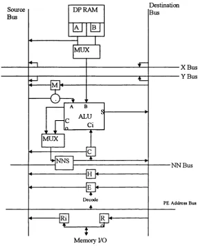
2.3.9 GEC Rectangular Image and Data (GRID)
The GRID is a prototype design o f an SIMD mesh array o f single PEs, each o f which
is physically connected to its four orthogonal neighbours. A neighbourhood
connectivity o f eight is achieved by routing information through one o f the orthogonal
links for diagonals in a single 100ns instruction cycle. The array controller was
designed to facilitate a pyramidal mapping o f image to processor where the image size
was greater than the number o f available PEs.
Processing Element
The 64 bits o f dual-ported RAM cache memory allow two operands to be read and
one output to be written to memory in a single instruction cycle (see figure 2.11). The
ALU supports the sixteen possible Boolean functions o f two variables and may also
be configured as a full adder with the carry appearing at C. This carry may then be
recombined locally or transmitted to a neighbour. The M register facilitates bit serial
multiplication and holds the current multiplier bit which is logically AN D ’ed with
each multiplicand bit before being added to the accumulator which is stored in the
cache memory. A special single bit register (H) is included for counting o f the number
o f ‘one’ bits in a particular image plane. All o f the H registers on a GRID chip are
joined as a continuous shift register whose contents can be clocked through a 16 bit
accumulator situated at the end o f the register which counts the number o f ones
present. The ACU then combines the chip results to give the total for the whole plane.
The E (enable) register is used to implement local activity control and can be set as
the result o f a calculation or by the PE addressing logic. Neighbour connections are
made via the NNS network. The array also contains the orthogonal X and Y data
buses similar to those in the DAP which can be used to broadcast information to the
whole array in a single instruction cycle. This information comes from either o f two
array edge registers that span the length and width o f the array and are written to by
the array control unit (These registers can also receive information from the array for
use by the ACU). Each PE can also access its own o ff chip memory via the R registers
Destination
Bus Source
Bus
X Bus Y Bus
N N B u s
Decode
PE Address Bus
NNS M UX
MUX
ALU
DP RAM
Memory I/O
Figure 2.9 The GRID PE
Input / Output
An I/O buffer is included in the system to allow easy transfer o f data to and from
peripheral devices (such as disks, monitors and cameras) which operate in a bit
parallel/word serial way whereas the array operates in a bit serial/word parallel way.
The buffer directly supports the pyramidal mapping o f data to the processing elements
and its input operation overlaps normal processing until a whole line is in place in the
buffer. Processing is then interrupted as the line is passed to the array via the Y bus.
Output o f data is achieved in a similar way.
GRID System Details Performance - Basic operations
Year 1985 Integer Addition 2.5ps
Developer GEC Integer Multiplication 10.3ps
Status Prototype System FP Multiplication (32 bits) 91ps
Topology 8-Mesh (logically) Binary Pointwise 0.12ps
PE: Bit Serial Performance - Neighbourhood operation
Array Size 8 x 8 Binary Near Neighbour 0.6|xs
Local Memory 64 bits Median Filter 1.1ms
Clock Rate 10 MHz Convolution (3x3 8 bits) 2.0ms
Long Range Com Ortliogonal Data Buses Binary Erode / Dilate 0.6fis
Table 2.8 GRID System Statistics