MEMS TECHNOLOGY AND
DEVICES FOR A MICRO FLUID
DOSING SYSTEM
Thesis by
Ellis Meng
In Partial Fulfillment of the Requirements for the Degree of
Doctor of Philosophy
California Institute of Technology
Pasadena, CA 91125
2003
© 2003
Ellis Meng
students do to hinder his efforts. Rodney Rojas and John van Deusen have helped me in the machine shop since my undergraduate years. They have managed to impart some machining experience and knowledge that has been invaluable in the completion of this thesis.
I also want to acknowledge Professor Joel Burdick, Professor Axel Scherer, Professor Ken Pickar, Professor Jerry Pine, Dr. Qiao Lin, Dr. Fukang Jiang, Dr. Amish Desai, Dr. Wen Hsieh, Ken Walsh, Dr. Nick Pornsinsirirak, Dr. Tze-Jung Yao, Dr. Yong Xu, Dr. Sang-wook Lee, Jun Xie, Victor Shih, Qing He, Dr. Yuji Suzuki, Edward Chiu, Howen Mak, Sascha Gassmann, Hans Hoeg, Dr. Brett Slatkin, Tanya Hefner, Janice Tucker, and Hung Bui for their help over the years.
I would like to thank my friends and family who have dragged me out of lab and provided me with some semblance of a life outside of work. My family has been extremely supportive and patient in putting up with me during this crazy time. I have many fond memories of adventures and laughs with Stephanie Pao and Frances Tice. Dr. Kim West and the Residence Life staff have given me the opportunity to try something completely different and for that I am grateful.
ABSTRACT
MEMS TECHNOLOGY AND
DEVICES FOR A MICRO FLUID
DOSING SYSTEM
Thesis by Ellis Meng
Doctor of Philosophy in Electrical Engineering California Institute of Technology
Microelectromechanical systems (MEMS) technology has matured to the point where practical
biological and chemical applications are possible. One particularly active research area is in the
development of lab-on-a-chip type systems. In order to create successful lab-on-a-chip and
other microfluidic systems, it is necessary to have the capability of controlling and directing
fluid flow. Such functionality can be found on the front end of a microfluidic system and is
known as a fluid delivery or dosing subsystem. For a MEMS micro fluid dosing system to be
realized, several components are necessary. The essential components include a fluid actuator,
a fluidic control device, and micro plumbing. A prototype fluid delivery system is
demonstrated here using a micropump as the fluid actuator, a thermal flow sensor as the
fluidic control device, and micromachined couplers as plumbing. The technology to build
these components has been developed and each of these components have been fabricated
and tested. A prototype constructed of discrete components has also been demonstrated. A
4.3.2 Process Flow 2... 117
4.3.2.1 Electroless Gold Plating... 121
4.4 Packaging... 122
4.5 Device Characterization... 123
4.5.1 Temperature Calibration... 123
4.5.2 Hot Film Mode Flow Testing... 125
4.5.2.1 Constant Current Operation ... 126
4.5.2.2 King’s Law... 129
4.5.2.3 Transient Response... 130
4.5.3 Calorimetric Mode Flow Testing... 131
4.5.4 Time-of-Flight Mode Flow Testing... 132
4.5.5 Bubble Detection... 133
4.6 Discussion of Multi-Mode Testing Results... 134
4.7 Summary... 135
CHAPTER 5
A MEMS Fluid Dosing System 139 5.1 Microfluidic Systems ... 1395.2 Dosing System Construction ... 140
5.3 Testing results ... 141
5.4 Discussion ... 142
5.5 Summary... 143
CHAPTER 6
LIST OF TABLES
Number Page
Table 1.1 A Brief History of MEMS ...3
Table 2.1 Thermal Expansion Coefficients of Common MEMS Materials... 27
Table 2.2 Physical and Thermal Properties of Parylenes [37]... 35
Table 2.3 Physical Properties of MRTV1 and Sylgard 184 ... 41
Table 2.4 Silicone Preparation Procedure... 41
Table 2.5 Summary of Pump Testing Results... 58
Table 3.1 List of Parameters Influencing Fluidic Coupler Design... 67
Table 3.2 Coupler Testing Results Compared to Other Work... 89
Table 4.1 Operational Modes of Thermal Mass Flow Sensors ... 104
Table 4.2 Mechanical, Physical, and Thermal Properties of Platinum ... 113
Table 4.3 TCR and Resistance Characteristics of Common Metals ... 113
Table 4.4 Process for Electroless Au Plating on Pt ... 121
CHAPTER 1
INTRODUCTION
The invention of the transistor in 1947 by John Bardeen and Walter Brattain of Bell Labs
marked the beginning of a revolution in electrical engineering that eventually led to the birth of
microelectromechanical systems (MEMS). Soon after this pivotal discovery, a research ensued
at a frenzied pace in the development of microelectronics resulting in the introduction of
commercial silicon transistors in 1954 and the invention of the first integrated circuit (IC) by
Jack Kilby of Texas Instruments in 1958. One of these early pioneers, Gordon Moore, made
an astute observation in 1965 that the number of components per IC would double every 2
years. Moore’s prediction, now popularly known as Moore’s Law, is not completely correct
and actually follows an 18-month doubling trend. Even so, this phenomenal growth rate
means that we are now able to enjoy personal computers that run on the computing power of
tens of millions of transistors in centimeter scale CPU packages [1]. The impact these
realm of engineering, the boom in microelectronic research has spun off countless new
technologies that are continually changing the way in which we engineer solutions to problems.
MEMS was inspired by the technologies used to create microelectronic devices. The
graduation from micro-electronic to electromechanical devices is a natural progression in the
technological evolution of the IC world.
1.1
THE BEGINNING OF MEMS
Perhaps one of the most notable historical events in the development of MEMS was when
Richard Feynman challenged the scientific community to explore the realm of miniaturization.
During his talk to the American Physical Society in 1959 dubbed “There’s Plenty of Room at
the Bottom,” Feynman pointed out the void in research done on “manipulating and
controlling things on a small scale.” He explained to scientists that this field “might tell us
much of great interest about the strange phenomena that occur in complex situations…a lot of
new things that would happen that represent completely new opportunities for design” and
that “it would have an enormous number of technical applications.” In order to properly
explore this field and be able to construct small machines, it would be necessary to design a
new set of infinitesimal machines that not only require scaling but also redesign. Ironically,
modern equipment used to construct semiconductor and MEMS devices is by no means
infinitesimal but there is hope in self-assembly and nanotechnology that these tiny machines
can be realized.
To further entice scientists to think about these issues, Feynman ended his talk with two $1000
competitions to the first person to print the information on the page of a book in an area
1/25,000 smaller in linear scale and to make a working electric motor measuring no more than
1.2 MEMS
TECHNOLOGY
The materials and techniques used in MEMS are continually evolving. MEMS technology is
still based largely on borrowed techniques from the semiconductor industry. Some processes
are essentially identical to their semiconductor industry analogs; however, other processes have
been adapted to suit the specific needs. The underlying focus of a semiconductor process vs. a
MEMS process can be drastically different to the extent that frequently it is not possible or
very difficult to integrate both electronics and MEMS on the same piece of real estate.
Microfabricated semiconductor devices are contained mainly within the top few microns of
the substrate material. MEMS devices may require the entire substrate thickness, utilize both
sides of the substrate, or even require bonding multiple substrates together. Over the years,
the spectrum of processes considered to be part of the MEMS toolbox has expanded greatly.
Traditional techniques are still very popular but are now accompanied by a host of newer ones.
1.2.1 F
UNDAMENTALMEMS T
ECHNIQUESMEMS has its roots in silicon-based devices from semiconductor fabrication. In addition to
silicon, alternative substrates such as metal, glass/quartz, ceramics, plastic, and silicone rubber
are gaining in popularity. Driving factors for this change are the desire to move towards
producing devices that are biocompatible, use cheaper materials, and are easy to fabricate from
both the process standpoint and when considering the required infrastructure to do so. Even
so, most devices are still fabricated in silicon because of its well-known electrical and
mechanical properties [5]. Silicon-based devices are also attractive in that there is a possibility
of integrating electronics next to MEMS devices on the same substrate.
The MEMS toolbox consists of a set of processes that based in silicon microfabrication
micromachining, LIGA, and wafer bonding. The majority of devices are still fabricated using
some combination of these techniques.
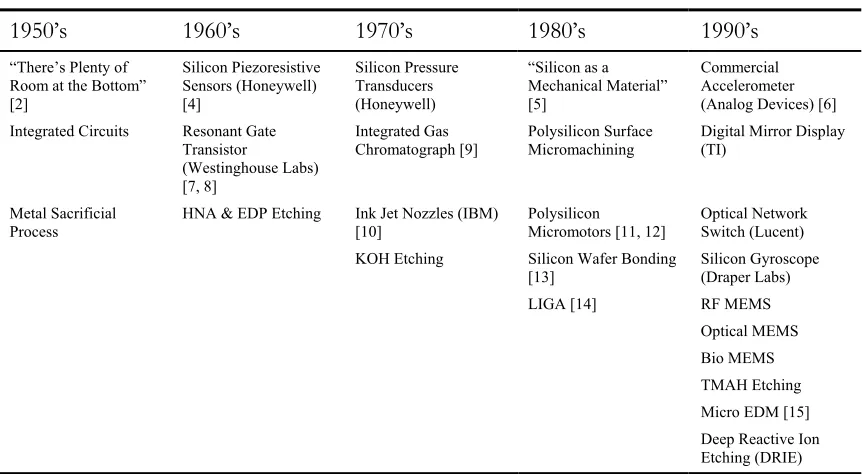
1.2.1.1 LITHOGRAPHY
Lithography is a method by which pattern transfer can be achieved from a master pattern to
the substrate. The fundamental idea is not a new concept and has in fact been employed by
artisans since the late 1700’s [17]. Lithography in some form is typically the first step in most
processes and, as a result, is probably the most important. Photolithography is the most
common technology used but in order to keep up with the demanding resolution needs of the
semiconductor industry, as alluded to by Moore’s Law, technologies such as X-ray lithography,
electron beam lithography, and ion beam lithography have been developed [18]. The basic
steps for photolithography involving positive and negative resists are shown in Figure 1-1.
Figure 1-1 Photolithography Process for Negative and Positive Resists
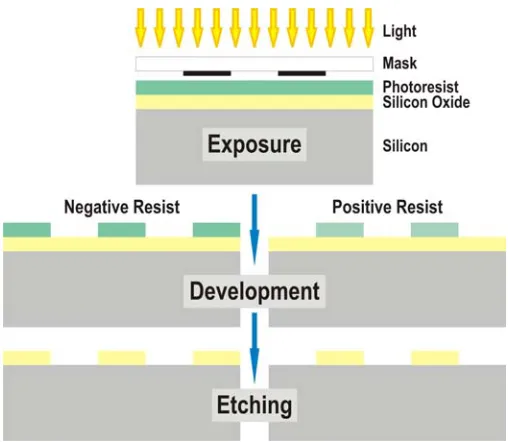
1.2.1.2 BULK MICROMACHINING
Bulk micromachining allows the production of structures carved out of the substrate.
chemical etching techniques. Some of these techniques allow etching through the substrate, to
fully utilize the entire substrate thickness. In addition, the crystalline nature of silicon can be
particularly advantageous when using certain wet etches. Both isotropic and anisotropic, or
orientation-dependent, wet etches are readily available (Figure 1-2 & Figure 1-3). Traditional
wet etch recipes include HNA (a hydrofluoric, nitric, and acetic acid mix), potassium
hydroxide (KOH), ethylenediamine-pyrocatechol-water (EDP), and
tetramethylammoniumhydroxide (TMAH) and are still a popular means of carving out
channels or creating membranes in silicon. Dry etching techniques such as plasma and gas
phase etching (XeF2 and BrF3) are also extensively used. Newer techniques, such as deep
reactive ion etching (DRIE) [19-21], allow structures with complex in-plane geometry and high
aspect ratios (> 20:1) to be fabricated (Figure 1-4). Even so, bulk micromachining is not
suitable to create all desired geometries. Devices requiring complex, multi-layer or multi-depth
structures are frequently difficult or not possible by bulk micromachining alone.
Figure 1-3 Anisotropic Wet Etching of Silicon
Figure 1-4 Anisotropic Dry Etching of Silicon via DRIE Using the Bosch Process
1.2.1.3 SURFACE MICROMACHINING
To create complex planar structures, it is necessary to use surface micromachining. Here,
alternating layers of structural and sacrificial materials are deposited and selectively removed to
achieve the desired results (Figure 1-5). As opposed to bulk micromachining, the substrate
may or may not be structurally significant in the final device and is often used only as a
mechanical support on which to build structural layers. Virtually any material that can be
including phosphosilicate glass (PSG), polysilicon, polymers (photoresist and polyimide), and
metals.
Figure 1-5 Basic Surface Micromachining Process
It is possible to build freestanding, released, and interlocking structures of any desired planar
geometry with surface micromachining. Surface micromachining examples include
electrostatic micromotors [11, 12], out-of-plane hinged structures [22-24], and springs [25].
However, only thin layers (≤ µm) of both the structural and sacrificial materials can be
deposited due to stress and other mechanical problems. Thus, the overall thickness of devices
created by surface micromachining is relatively thin. In addition, sometimes devices are
plagued by stiction.
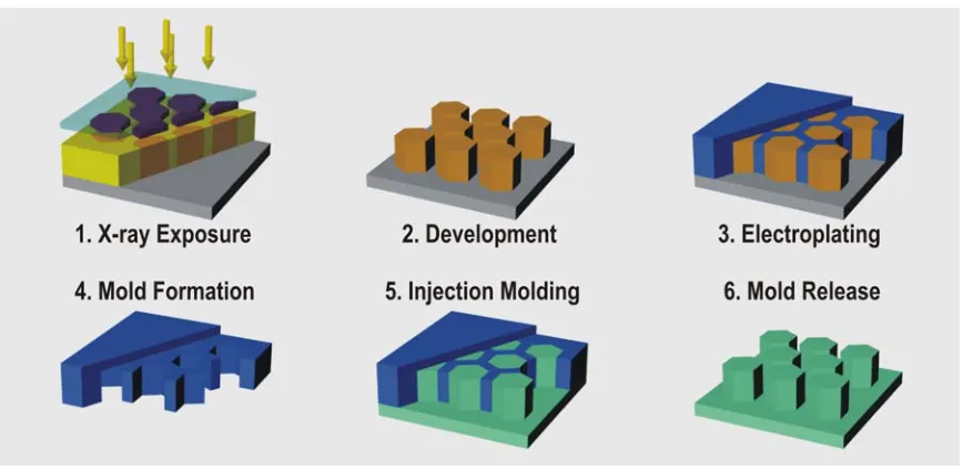
1.2.1.4 LIGA
LIGA was initially developed in 1982 for the fabrication of micron-sized separation nozzles
for nuclear power production applications in Germany [14]. The name is actually derived
from the German acronym for “X-ray lithographie galvanoformung abformung, ” which
Figure 1-6 shows a typical LIGA process. Thick x-ray resist is exposed and used as a mold for
electroplating. This newly formed metal mold can then be used to injection mold plastic parts
or more plastic molds. High aspect ratio structures ranging from microns to centimeters in
height with high resolution (< 0.2 µm) can be formed in this manner. An assortment of
devices such as accelerometers [26], optical couplings [27], and microfluidic devices [28] have
been fabricated using LIGA. While the capability of producing three-dimensional structures
using LIGA is attractive, LIGA is a costly process due to the synchrotron source required for
x-ray exposure and x-ray masks. Thus, less expensive means of producing the same results are
being investigated.
Figure 1-6 Typical LIGA Process
1.2.1.5 WAFER BONDING
Wafer bonding is a convenient means of permanently joining wafers together and
circumventing the wafer thickness limitation on devices. It also gives a means to create
multi-level devices by combining wafers processed using bulk or surface micromachining or even
sealing. The three most common forms of bonding are fusion bonding (silicon-to-silicon) [19,
29, 30], anodic bonding (silicon-to-glass) [31-33], and eutectic bonding (silicon-to-gold) [34].
Historically, glass-to-metal bonding has been investigated as early as 1969 [35]. The high
pressure, temperature, or voltage requirements of certain bonding processes may not be
compatible with all devices.
1.2.2 N
ON-T
RADITIONALMEMS T
ECHNIQUESAdding to the wealth of variety in the micromachinist’s processing toolbox are a number of
non-conventional micromachining techniques that have been developed over the years. The
desire to create truly three-dimensional structures has lead to the development of micro EDM
[15, 36-38], laser micromachining [39, 40], and 3D stereolithography [41, 42]. With the
ever-increasing demand for biocompatible devices, plastics have becoming more popular as are
techniques to process them are more readily available. Injection molding [43, 44] and
compression molding/hot embossing [45, 46] can be used to fabricate inexpensive plastic parts
quickly and in high volume. Another inexpensive and fast process is the “soft lithography”
[47, 48] of compliant silicone rubber structures. This technique has become particularly
popular in the microfluidics field. As always, man looks back to nature for inspiration; self
assembly [49] hopes to bring micromachining to a new level by taking advantage of naturally
occurring biological and chemical processes to assemble useful devices and structures.
1.3
MEMS FOR MICROFLUIDICS APPLICATIONS
Much of the attention on MEMS in recent times has been devoted to the development of
microfluidics. Biosensors and other tools for chemistry and biology are among the many
exciting applications of microfluidics. These efforts are frequently referred to as lab-on-a-chip
The need for technology to produce devices capable of high throughput, low volume
consumption, and producing accurate results already exists in genome sequencing and drug
analysis. While these reasons are compelling, miniaturization of systems can also provide
impetus for continued progress in microfluidics. Many laboratory techniques common to
chemistry and biological require time consuming repetition of many tasks. With microfluidic
technology, it is possible not only to miniaturize one specific process, but also to combine a
multitude of functionality into one chip level system. By seamlessly integrating tasks such as
sample preparation, sample reaction, and product detection, it is possible to speed up
processes dramatically. In addition to automating processes, microfluidics offers the
possibility of the conduction of massively parallel processes.
Lab-on-a-chip systems may consist of a number of components in a variety of subsystems
(Figure 1-7). In general, inputs are converted to the desired outputs through a network of
fluidic channels and may encounter a combination of sample preparation stages, reaction
chambers, or detectors during this process. While each specific application may require
different arrangements of the subsystems, one common element in all of these systems is a
fluid delivery and transport mechanism. The ability to control, monitor, and direct flow in a
precise and meaningful manner is crucial in the development of practical microfluidic systems
for biological and chemical processes.
Many have demonstrated individual devices that are required in a fluid delivery system but
complete systems are lacking. In an effort to realize lab-on-a-chip systems, a micro fluid
dosing system has been developed. The essential components are a fluid actuator, a fluidic
control device, and micro plumbing. MEMS components that were chosen for the
(Chapter 3), and a micro thermal flow sensing array (Chapter 4). Each piece of the system has
been designed, fabricated, and tested prior to implementation in a fluid dosing system (Chapter
5).
Figure 1-7 Overview of a Typical Lab-on-a-Chip System
[43] Larsson, O., O. Öhman, Å. Billman, L. Lundbladh, C. Lindell, and G. Palmskog, Silicon Based Replication Technology of 3D-Microstructures by Conventional CD-Injection Molding Techniques, in Transducers '97. 1997: Chicago, IL. p. 1415-1418.
[44] Despa, M.S., K.W. Kelly, and J.R. Collier, Injection molding of polymeric LIGA HARMs. Microsystem Technologies, 1999. 6(2): p. 60-66.
[45] Becker, H. and U. Heim, Hot embossing as a method for the fabrication of polymer high aspect ratio structures. Sensors & Actuators A, 2000. 83(1-3): p. 130-135.
[46] Heckele, M., W. Bacher, and K.D. Müller, Hot embossing - The molding technique for plastic microstructures. Microsystem Technologies, 1998. 4(3): p. 122-124.
[47] Xia, Y.N. and G.M. Whitesides, Soft lithography. Annual Review of Materials Science, 1998. 28: p. 153-184.
[48] Qin, D., Y. Xia, J.A. Rogers, R.J. Jackman, X.-M. Zhao, and G.M. Whitesides, Microfabrication, Microstructures and Microsystems. Topics in Current Chemistry, 1998. 194(5369): p. 1-20.
CHAPTER 2
A MICRO DIAPHRAGM PUMP
Inasmuch as pumping is still the primary means of fluid transport for microfluidic systems
today, micropumps are perhaps the most extensively researched topic in microfluidics. With
the drive to apply microfluidic solutions to research in genomics, proteomics, and drug
discovery, micropump research is focused on producing a practical solution for providing the
controlled and accurate transport of fluids. Various actuation and pumping methods have
been explored as a solution to moving fluids on the micro scale. Even so, the controlled
transport of fluids is critical but not yet practical by micropumps. Also, a fully integrated
solution for microfluidics still does not exist; methods presented thus far still have inherent
limitations. The two generations of pumps presented here are primarily targeted at moving
Figure 2-1 Micro Diaphragm Pump Components
2.1.2.2.2 PERISTALTIC PUMPS
Peristaltic pumps operate based on the peristaltic motion of sequentially arranged pumping
chambers (Figure 2-2) [16]. This motion squeezes fluid from one point to another. Although
they structurally simplistic compared to diaphragm pumps, which require check valves, reverse
leakage can be a major problem for peristaltic pumps. The planar layout of such pumps allow
for ease of fabrication and assembly but multiple actuators with control electronics are
required to drive these pumps. Several MEMS implementations of peristaltic pumps have
been explored (Figure 2-3) [9, 10, 17]. Large stroke volume and compression ratio are
strategies for improving peristaltic pumps.
High η is required for good flow directing capability. As suggested by lack of reverse flow
blocking elements, valveless pumps are prone to leakage and back flow. It is important to
maximize stroke volume and minimize dead volume when designing valveless pumping
systems.
Figure 2-4 Valveless Pump Operation
2.1.2.2.4 ROTARY PUMPS
Rotary pumps potentially can be use to pump viscous fluids at the micro-scale [20, 21].
However, the large loads make an integrated actuator impractical. Also, the complexities
involved in fabricating high aspect ratio rotating gears makes these types of pumps
unattractive. Although these pumps can potentially be self-priming, leakage effects can prove
difficult to overcome during assembly.
2.1.2.3 DYNAMIC PUMPS
Dynamic pumps are further divided into ultrasonic and centrifugal pumps.
2.1.3 N
ON-M
ECHANICALP
UMPINGS
CHEMESNon-mechanical pumps require the conversion of non-mechanical energy to kinetic energy to
supply the fluid with momentum. These phenomena are practical only in the micro-scale.
Thus practical flow rates for non-mechanical pumps start at 10 µl/min and below [7].
electrokinetic [1, 25], magnetohydrodynamic (MHD) [3, 4], and surface tension driven pumps
[26-28].
2.2
DESIGN AND FABRICATION
Mechanical pumping is ideal for operation in presence of particulates, multi phase fluids, and
for its immunity to properties of the flow. In the micropump realm, mechanical pumps have
been well studied. While diaphragm pumps are somewhat complicated to fabricate, they have
the potential to deliver large amounts of flow. The limiting factor is typically the actuator.
Micro actuators are restricted to small strokes so to utilize the flow throughput potential of
micropumps, external actuators are required. Here, a diaphragm pump with an external
actuator is presented. The design aims are to maximize actuator deflection, and thus stroke
volume to explore higher flow rates than typically achieved by micropumps (> 1 ml/min).
This diaphragm pump has gone through two iterations of the design process. Significant
improvements were made from one generation to the next as individual components were
completely redesigned. Micropumps, by nature, are composed of a significant number of
components that are difficult to fabricate in a completely integrated manner. Thus, the
approach here is to create modular components that can be clamped together to form a pump.
This prototyping method facilitates pump characterization.
2.2.1 P
ARYLENEC
HECKV
ALVESCheck valves are rectifying fluidic elements and share an equivalent function to diodes do in
electrical circuits. Ideally, a check valve permits flow when exposed to forward fluid stream
and inhibits flow for a reverse one. However, a finite cracking pressure is required to initiate
forward fluid flow and most implementations exhibit some amount of reverse leakage flow
large reverse pressures. Various implementations of check valves have been investigated
including rectifying structures created from ring mesas [13], cantilevers [29], membranes [30],
discs [31], V-flaps [32], and floats [33] (Figure 2-6). These valves are constrained to operate
within a specific flow range. This is in large part due to the excessive flow resistance to
forward flow experienced across the valve cap and valve seat. As shown in Figure 2-6, MEMS
check valves used in micropumps will result in out-of-plane flow. Planar check valves have
not been extensively researched and are currently not optimized for use with micropumps [34].
Figure 2-5 Check Valve Behavior [35]
Figure 2-6 Check Valve Types Found in Literature [35]
To reduce the forward flow resistance, an elastic material and appropriate valve cap geometry
are chosen. In this approach, parylene C check valves from [36] were used in the first pump
design. Large valve cap deflections are possible as parylene has a low Young’s modulus (~2.8
GPa) and S-shape tethers allow the valve cap two degrees of freedom. Flow resistance and,
elevate away from the valve seat (Figure 2-7). In addition, reverse leakage is extremely low as
valve-cap-to-valve-seat sealing is excellent and high reverse pressures can be tolerated. The
overall performance is further enhanced by the immunity to stiction and surface tension
effects. However, since these check valves were fabricated on the same side of the wafer, they
are only able to rectify flow in one direction. In order to construct a pump from these valves,
complicated assembly was required to separate individual valves and glue them, facing in
opposite directions, to a Plexiglas structural support. As a result, in the second design, check
valves were fabricated using a process modified from [36] to create a double-sided valve chip
(Figure 2-8). In addition, linear arrays of check valves were also fabricated using the same
process.
Figure 2-7 Parylene S-Tethered Check Valve Operation [35]
Figure 2-8 Two Types of Fabricated Double Sided Check Valves
2.2.1.1 PARYLENE FUNDAMENTALS
Parylene is the generic name for a family of unique vapor phase deposited thermoplastic
and biocompatibility are factors in its increasing popularity as a MEMS material. Excellent
dielectric properties have resulted in extensive use of parylene in semiconductor processing as
well. Three kinds of parylene are available commercially and each material has slightly
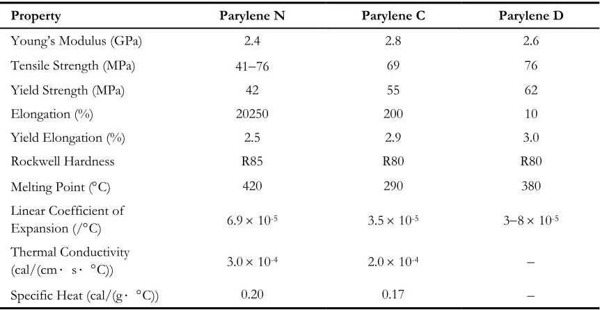
different properties for flexibility in application (Figure 2-9). A comparison of parylene N, C,
and D is shown in Table 2.2. Parylene C is the most commonly used form for its useful
combination of physical and electrical properties.
Figure 2-9 Types of Commercially Available Parylene
Table 2.2 Physical and Thermal Properties of Parylenes [37]
Property Parylene N Parylene C Parylene D
Young’s Modulus (GPa) 2.4 2.8 2.6
Tensile Strength (MPa) 41−76 69 76
Yield Strength (MPa) 42 55 62
Elongation (%) 20250 200 10
Yield Elongation (%) 2.5 2.9 3.0
Rockwell Hardness R85 R80 R80
Melting Point (°C) 420 290 380
Linear Coefficient of
Expansion (/°C) 6.9 × 10⁻⁵ 3.5 × 10⁻⁵ 3−8 × 10⁻⁵
Thermal Conductivity
(cal/(cm⋅ s⋅ °C)) 3.0 × 10⁻⁴ 2.0 × 10⁻⁴ −
2.2.1.2 PARYLENE PROCESSING
Parylene was discovered by Michael Mojzesz Swarc at the University of Manchester in 1947.
Later, in the 1950’s, research to develop a commercial parylene deposition process was
initiated by William F. Gorham of the Union Carbide Corporation. A coating system was
finally introduced to the market in 1965. Although only three kinds of parylene are
commercially available, it is interesting to note that Union Carbide developed over 20 different
types [38]. The finalized synthetic process involves the vapor phase deposition of parylene
from its dimer form (Figure 2-10). The dimer (di-para-xylylene) is a stable compound that
comes in granular form.
The first step of the deposition process vaporizes the dimer at 150 °C. Then pyrolysis occurs
causing the dimer to be cleaved into a monomer radical (para-xylylene). This monomer
adsorbs and polymerizes when it reaches the room temperature deposition chamber. The
deposition rate of parylene C is about 5 µm/hr. All depositions of parylene were performed
using the PDS 2010 Labcoter® 1 from Specialty Coating Systems.
A convenient feature of parylene is that it integrates well into MEMS processes. Oxygen
plasma etching conveniently patterns the material using either an Al or photoresist masking
layer. In addition, adequate adhesion to silicon and silicon oxide are achieved by applying a
special adhesion promoter (A-174) prior to deposition.
2.2.1.3 PARYLENE CHECK VALVE FABRICATION
The fabrication process starts with a thermally oxidized (1.5 µm thick) silicon wafer (Figure
2-11). This layer serves as a simply etching mask. The first structural feature to be defined is
the orifice. However, as subsequent processing is necessary in these areas to form the valve
cap, only a cavity is etched and not a through hole. Cavities are etched using KOH. The
remaining 20 µm thick silicon membrane serves as a structural support on which to build the
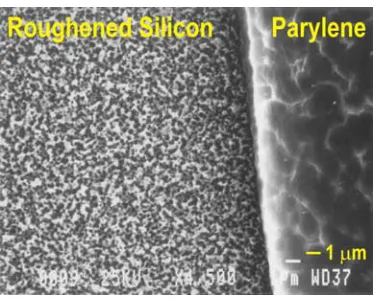
check valves. A circular region of silicon is then exposed to BrF3 gas for the purpose of
roughening the surface via etching [39]. This roughened silicon surface serves two purposes:
(1) it prevents stiction of the parylene tethers to the substrate and (2) it enhances the adhesion
of the anchored portions of the parylene tethers to the silicon substrate by increasing the
contacted surface area (Figure 2-12). A-174 adhesion promoter is applied and followed by the
deposition of a 2 µm layer of parylene-C. This layer is patterned in oxygen plasma to form a
circular support ring for the valve cap layer. Then a sacrificial photoresist layer (5 µm of AZ
4400) is spun and patterned to separate the valve cap from the valve seat. To prevent check
valve failure due to mechanical failure from stresses experienced at sharp corners, the
photoresist is hard baked to round off the convex corners as depicted in Figure 2-13. A
second layer of parylene (3 µm) is deposited and masked with a 1000 Å layer of thermally
evaporated aluminum. This Al masking layer was replaced with thick photoresist (10 µm of
the high temperatures of the thermal evaporation process. To release the check valves, the 20
µm silicon layer between the eventual orifice and sacrificial photoresist layer is etched away in
BrF3 gas. After dicing, the Al/photoresist masking layer and sacrificial photoresist layer
areremoved to complete the fabrication process. Various views of the fabricated check valves
are shown in Figure 2-8 and Figure 2-14.
Figure 2-11 Double Sided Check Valve Fabrication Process
Figure 2-13 Rounded Photoresist Step After Hard Baking
Figure 2-14 SEMs of Fabricated Check Valves
2.2.2 S
ILICONER
UBBERP
UMPINGM
EMBRANEDesired properties of pumping membranes are large deflection and good sealing. In addition,
to improve the achievable compression ratio, a material that will allow the deflected membrane
to efficiently match and conform to the pumping chamber geometry is needed. Silicone
rubber has low Young’s modulus and durometer, as well as high elongation. These properties
2.2.2.1 SILICONE RUBBER FUNDAMENTALS
Silicone is a general term that refers to a diverse class of partially organic polymers that can be
found in multiple forms including elastomers, resins, and liquids. The most notable difference
of silicone from most polymers is that is formed from a silicon-based backbone, not a carbon
one. This contributes to the excellent chemical stability and electrically insulating properties
valued in this family of materials. Structurally speaking, silicone is composed of a chain of
alternating silicon and oxygen atoms (a polysiloxane chain) with hydrocarbon radicals
occupying the remaining silicon valences (Figure 2-15). The radical is typically a methyl group
(−CH3) as in polydimethylsiloxanes (PDMS).
Figure 2-15 A Linear Polysiloxane Chain
The particular type of silicone chosen for the pumping membrane is MRTV1-10E. This is
manufactured by Insulcast, a division of American Safety Technologies, and is a room
temperature vulcanizing (RTV), addition cure mold making silicone rubber. This particular
formulation has a 10% reactive fluid dilution, which has been found to facilitate its application
via spin coating and exhibits good adhesion to silicon and silicon nitride [40]. Typical physical
parameters are given in Table 2.3. Addition cure vulcanized silicone rubber typically starts as a
two-part mixture consisting of a base and curing agent. The curing agent contains a
crosslinker. By slightly altering the amount of crosslinker applied in a mixture, the physical
properties of the cured silicone can be modified. The recommended mixing ratio for
for adhesion to MRTV1. Silicone is spun on this surface and then the entire structure is cured.
The remaining silicon is etched away via RIE (reactive ion etching) in a SF6/O2 plasma to free
the membrane. Alternatively, a silicon nitride masking layer can be used.
Figure 2-16 A Simple Silicone Membrane Process [40]
A refinement on the above process is shown in Figure 2-17. In this modified process, pillars
are integrated in the membrane layer to control the compression of the rubber layer when
exposed to clamping force. This process also avoids thickness control difficulties encountered
when applying the silicone in a spin coating process. The pillars are formed during an
additional patterning step followed by KOH etching. The masking material can be identical to
the one used in forming the silicon membrane. Instead of spin coating, the silicone layer is
applied by casting. Membranes created using this technique measure 7 × 7 mm2 and are 80
µm thick. One is shown in Figure 2-18.
Figure 2-18 Fabricated Silicone Membrane with Pillars
The previous processes all result in square membranes due to the anisotropic etching of
silicon. In order to achieve a circular geometry, it is necessary to use deep reactive ion etching
(DRIE) to produce the membrane. Circular pumping membranes are able to achieve better
compression ratios and thus better pump performance. DRIE is also ideal for creating circular
bosses. Bossed membranes can further improve pumping efficiency. Wet anisotropic etching
would required complicated mask geometries to achieve a similar structure.
The process flow for fabricating circular silicone membranes is shown in Figure 2-19. Thick
photoresist (AZ 4620) is spun and patterned to define the membrane. Thermal oxide can also
be used as a mask, however, there is an additional step required to remove the front side oxide
prior to the application of silicone. A brief descum in oxygen plasma followed by an HF dip
(10 % hydrofluoric acid) is necessary to prevent micrograss formation during DRIE etching.
Wafers are then etched via DRIE until a thin silicon membrane (~20 µm thick) remains.
Silicone rubber is spun on the backside at 1 krpm for 80 seconds to yield an approximately 140
µm thick membrane layer when cured. The remaining silicon is etched away via RIE (reactive
ion etching) in a SF6/O2 plasma. Circular diaphragms with and without bosses (5, 6, and 7
mm in diameter) and measuring 8 mm in diameter where created using this procedure. They
Figure 2-19 Circular Silicone Membrane Fabrication Process
Figure 2-20 Fabricated Circular Membranes
2.2.3 S
ILICONER
UBBERG
ASKETSAs previously mentioned, silicone rubber is a suitable material for sealing purposes. Several
levels of silicone gaskets were fabricated in the second pump design to seal the assembled
pump and serve as spacers. The physical properties of the silicones used are presented in
Table 2.3
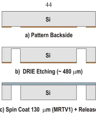
2.2.3.1 CHECK VALVE TO PUMP SEAT GASKET
Silicone gaskets were introduced in the second pump to seal the check valves to the pump
seat. A molding technique is used to create gaskets whereby silicone is molded into a DRIE
etched silicon master, cured, and then release from the mold (Figure 2-21). The gasket is
the Plexiglas pump seat. 10 µm of photoresist (AZ 4620) is spun and patterned to define the
alignment pegs. After a brief descum in oxygen plasma and an HF dip, the wafer is etched to a
depth of ~ 300 µm via DRIE. A second lithography (10 µm AZ 4620), descum, and HF dip
are performed to define the gasket boundaries. Both features are etched together to establish
the thickness of the gasket (~ 100 µm) and finalize the height of the pegs (~ 400 µm). Prior
to silicone molding, a mold release layer of Parylene or plasma deposited Teflon (CHF3) can be
applied. Sylgard 184 is used for its transparency. Molding is achieved by filling the mold with
a layer of silicone precursor and using a flat blade to squeegee the excess material away. This
technique is similar to a molding technique used in fabricating valve membrane elements in
[41]. The mating alignment structures between the pump seat and gasket can be seen in Figure
2-22.
Figure 2-22 Alignment Structures on a Fabricated Gasket and Machined Pump Seat
2.2.3.2 CHECK VALVE TO PUMP CHAMBER GASKET
One complication in using check valves with large cap deflections in a diaphragm pump is that
additional structural layers are necessary to prevent damage to the check valves. To prevent
silicone membranes from adhering to the check valves during pump operation, a
conventionally machined Plexiglas spacer was included in the second pump design. This,
however, creates the need for another silicone gasket to seal the spacer to the check valve chip
(Figure 2-23). Taking into account the gasket thickness requirement based on the Plexiglas
spacer thickness and additional height required to prevent membrane-check valve contact (>
500 µm), it is impractical to use a silicon wafer as the mold master for this gasket. Therefore,
these gaskets were molded from precision milled Delrin masters. Delrin is similar to Teflon
and thus no mold release layer is required. Sylgard 184 was used again for its transparency and
applied in exactly the same manner as described for the check valve to pump seat gasket. For
the check valve array case, it is difficult to make a machined master for due to tight spacing.
Large openings for the check valve array were machined into the master so through holes for
Figure 2-23 As-Molded Silicone Check Valve to Pump Chamber Gaskets
2.2.3.3 PUMP CHAMBER SPACER AND GASKET
The first generation spacer is simply an 8 × 8 mm2 orifice etched through a silicon substrate via
KOH. The front side is glued to the pump body and the backside is clamped to the pump
membrane. Second generation pump spacers are conveniently formed by carefully cutting out
the released circular membrane portion of the membrane chips (Figure 2-24). They serve to
seal the pumping chamber from leaks as well as define the height of the chamber.
Figure 2-24 Circular Pump Chamber Spacer and Gasket
2.2.4 E
XTERNALA
CTUATORSThe choice to go with an external actuator in this design can be understood by evaluating the
current state of art in micro actuator technology. The deflections desired are on the order of
actuator based on the discussion earlier. Ideally, the actuator should have a maximum vertical
deflection of 500 µm over a wide range of frequency.
2.2.4.1 SOLENOID VALVE CONTROLLED PNEUMATIC ACTUATION Pneumatic actuators are a possibility as the membrane deflection is not physically limited by
actuator travel but by the pumping chamber dimensions. Hence, it is useful to characterize the
pump using pneumatic actuation. An external compressed air source and a Clippard ETO-3-6
three-way solenoid valve are connected together to supply bursts of pressurized air to the
pump. One major drawback of this method is that the restoring force experienced by the
membrane is solely due to the physical properties of the material from which it is made.
2.2.4.2 SOLENOID PLUNGER ACTUATOR
Another possibility is to use a solenoid actuator. A modified version of the solenoid found in
[42] can be made to give deflections of ~ 250 µm (Figure 2-25). The solenoid actuator
contains a plunger that is made to produce a reciprocating motion when the supply current to
the solenoid is turned on and off (Figure 2-26). The plunger is fully extended when no power
is applied by a spring element in the body of the solenoid. When the coil is supplied with
current, the induced magnetic field creates a force that retracts the plunger into the body.
Thus, in this manner, the restoring force is not completely dependent on the membrane
material properties. The plunger can also be outfitted with various tips (Figure 2-27). Special
Figure 2-25 Cross Section of Solenoid Actuator
Figure 2-26 Solenoid Actuation Scheme
Figure 2-27 Two Types of Tips Used on the Solenoid Actuator
2.2.5 A
SSEMBLY ANDP
ACKAGINGPump prototype assembly involves the use of Plexiglas pump seats in addition to a
combination of gluing and clamping. The first generation pump was constructed by gluing the
generation was designed to eliminate the need for glue by taking advantage of the sealing
property of silicone rubbers. Alternating layers of silicone and silicon allowed the pump to be
watertight when clamped.
The first generation pump was assembled through a combination of clamping and gluing
(Figure 2-28). The membrane chip was glued to a Plexiglas plate and clamped to the rest of
the pump, which consisted of chips stacked and glued together. Tygon tubing was connected
to the input and output to facilitate testing. A solenoid actuator was then properly positioned
beneath the membrane.
Figure 2-28 Various Views of the 1st Generation Solenoid Driven Pump
The second generation pump was entirely clamped and only required adhesive to connect the
tubing and actuator to the packaging (Figure 2-29 & Figure 2-30). This modular design allows
easy access to and replacement of individual components. Two different pump seats were
precision milled from Plexiglas for the two different check valve configurations. Plexiglas
backing plates allowed the pump to be clamped together and provided a means for attaching
the actuator. A different backing plate was used during pneumatic testing to allow for
Figure 2-29 Clamped Pump Chamber Structure
Figure 2-30 Various Views of Clamped Pumps
2.3 PUMP
CHARACTERIZATION
2.3.1 C
HECKV
ALVEP
ERFORMANCECheck valves (orifice dimensions of 780 µm × 780 µm) used in the first generation pump have
been thoroughly tested and analyzed in [36]. Performance of the double-sided check valves
was characterized for both air and water. Flow rate versus applied pressure plots with the
check valve in place and removed (orifice only) were obtained (Figure 2-31). As shown in [36],
the twist-up tether configuration of the check valves allows for enough deflection to achieve
nearly atmospheric pressure at the exit. Thus, flow resistance induced by the valve cap is
negligible. In comparison to valves of similar size designed with straight tethers, the
membrane deflection owing to S-shaped tethers can be up to four times as high. Check valve
BrF3 roughened silicon surface underneath the valve cap inhibits stiction and surface tension
effects from interfering with valve performance.
Figure 2-31 Single Check Valve Testing Results
Figure 2-32 Check Valve Array Testing Results
Check valve arrays, consisting of an inlet and outlet with three individual check valves each,
were also characterized. Figure 2-32 shows the flow rate increase as the number of check
valves was increased. It is evident from Figure 2-33 that a slight advantage in performance for
check valves are 770 µm × 770 µm and for each of the check valves in the array, 370 µm ×
370 µm. Effective orifice areas are 5.93 × 10⁻³ mm2 and 4.11 × 10⁻³ mm2, respectively. Thus, a
check valve array is preferred over a single check valve design to maximize flow rates and
decrease flow resistance.
Figure 2-33 Comparison of Check Valve Schemes
2.3.2 P
NEUMATICA
CTUATIONE
XPERIMENTSPneumatic actuation was utilized to verify the design of the second generation pump (Figure
2-34). Bursts of compressed air are supplied to control the deflection of the pumping
membrane by turning on and off a three-way solenoid valve. This pattern of actuation can
Figure 2-34 Pneumatic Testing Fixture Schematic
Both check valve schemes were tested using an inflation pressure of 6.9 kPa that is regulated
by the solenoid valve. The flow rate of deionized water was determined by timing the passage
of a bubble through a calibrated pipette downstream from the pump outlet. A maximum flow
rate of 4.4 µl/min at 13 Hz and back pressure of 3.6 kPa at 5 Hz were possible with the single
inlet and outlet design (Figure 2-35). A nearly threefold increase in achievable flow rate of 13
µl/min at 11 Hz and back pressure of 5.9 kPa at 5 Hz were made possible by the array pump
(Figure 2-36). Thus, the check valve array pump outperformed the single check valve pump in
both categories. Nonlinear behavior in the flow rate dependency on frequency was observed.
This is expected as the silicone membrane takes a finite time to return to its original, relaxed
position after being deflected. When the frequency of air bursts increases beyond the
necessary relaxation time of the membrane material, the efficiency of the pump decreases
dramatically. This validates the need for an additional restoring force to operate the pump at
higher frequencies and to achieve higher flow throughputs. It is unfortunate that pneumatic
actuation cannot be easily optimized to overcome these problems as it provides the best means
of attaining the maximum possible stroke volume, which in turn would lead to the best
possible compression ratio. No other means of actuation currently available can provide these
Figure 2-35 Pneumatic Testing Results of Single Check Valve Pump
Figure 2-36 Pneumatic Testing Results of Check Valve Array Pump
2.3.3 M
ECHANICALA
CTUATIONE
XPERIMENTSSolenoid actuation produces a reciprocating motion in which an integrated plunger is retracted
and extended as current is turned on and off, respectively. By using the plunger to deflect the
silicone membrane repeatedly, water pumping is achieved. During solenoid based actuation
tests of the micropumps, the actuator was driven using an 11 V square wave signal at various
frequencies. This translates into a power consumption of about 700 mW. An assembled
control of and connection to a power source. Again, the flow rate of deionized water was
determined by timing the passage of a bubble through a calibrated pipette downstream from
the pump outlet. Flow rate versus frequency and back pressure plots are displayed in Figure
2-38. This pump is not self-priming and so careful priming is necessary to achieve optimal
performance. As expected, flow rate is highly dependent on actuation frequency and is
approximately linear for low frequencies. However, above 10 Hz, this linear relationship is lost
as the membrane is unable to respond at the speed at which the plunger is actuated. The
maximum achievable flow rate was 3.4 µl/min at 10 Hz and maximum sustainable back
pressure was 2.1 kPa which occurs for both 10 and 20 Hz.
Figure 2-37 Solenoid Actuated Pump Testing Fixture and Schematic
To eliminate the fall off in flow rate at high frequencies, it is necessary to physically connect
the actuator to the pumping membrane. This provides an additional restoring force to pull the
membrane back to its relaxed state after being actuated. Thus, a new membrane with a circular
silicon boss structure (7 mm in diameter) was implemented in the second design. The surface
of cured silicone is inert and not easily bonded to. In order to physically connect the plunger
of the actuator to the pumping membrane, a boss structure is necessary. Figure 2-27 shows a
7mm silicon boss is glued to a flat aluminum plunger. The improvement in flow rate versus
frequency performance for the single inlet/outlet pump is shown in Figure 2-39. As expected,
the flow rate vs. frequency relationship is linear at lower actuation frequencies, and at a critical
frequency, the flow rate levels off as it limited by the maximum fluid flow that can be supplied
by the check valves. The additional load placed on the actuator from the physical coupling to
the silicone membrane probably affects the pump output to some extent. A maximum flow
rate of 4.5 µl/min at 14 Hz was possible in this configuration. However, the maximum back
pressure decreased slightly to 1.32 kPa at 1 and 5 Hz.
pressure drop over the fluidic resistance (Q P R= fluid), the volume pumped per cycle is
inversely proportional to the frequency. Solenoid actuation, in which the membrane and
plunger are physically connected, produces a more complicated behavior that cannot be
completely described by this simple analysis. The data suggest that the membrane deflection,
which occurs in a finite amount of time, might be a contributing factor as it also decreases with
increasing frequency.
Figure 2-40 Volume Pumped Per Cycle vs. Frequency of the Various Pumps
For the pumps presented, a solenoid actuator was sufficient to demonstrate the device.
However, integrated actuators, perhaps either thermopneumatic or piezoelectric ones, would
provide a more practical solution for an integrated system. The pump footprint would be
piezoelectric actuators have their advantages and disadvantages as discussed earlier in the
chapter. Although much knowledge has been gained on micropumps, much work remains to
be done to achieve a practical MEMS micropump for integrated fluidics applications.
2.5 SUMMARY
Two generations of check-valved silicone rubber diaphragm pumps are presented. Significant
improvements have been made from pump to pump including the design and fabrication of a
double-sided check valve, a bossed silicone membrane, and silicone gaskets. For the first time,
check valve arrays were implemented in a micro diaphragm pump. Water flow rates of up to
13 ml/min and a maximum back pressure of 5.9 kPa were achieved through pneumatic
operation with an external compressed air source. Using a custom designed solenoid actuator,
flow rates of up to 4.5 ml/min and a maximum back pressure of 2.1 kPa have been
CHAPTER 3
MICROFLUIDIC COUPLERS
MEMS devices bring forth new challenges in the interconnectivity between the micro and
macro worlds. The microelectronics world has relied heavily on advances in the packaging
industry for technological advancement. Without novel breakthroughs in microelectronic
package engineering, the continued miniaturization of electronics would not be possible.
Microelectronic packages are constantly shrinking and quickly approaching sizes on the order
of the device they are protecting. Perhaps one day, fabrication and packaging will be
integrated and devices will be ready to plug in and use as soon as they are diced and separated
from the wafer! The MEMS world is, however, far from reaching this ideal. While electrical
connections are also important in MEMS, a comprehensive packaging technology does not
exist. In addition to electrical connections, MEMS devices often require another means of
communicating with the environment. For example, it is necessary to provide mechanical
confounding example of this dilemma is found in the microfluidics field. The incompatibility
of simultaneous electrical and fluid connections is a problem has not been solved. Many
difficult issues exist in defining the connections of micro-devices with the surrounding
environment.
3.1
THE NEED FOR MICROFLUIDIC COUPLERS
Micromachined fluidic devices are posed to have a great impact on the field of biology and
chemistry. The benefits of adopting microfluidic techniques are many including laminar fluid
flow, minimal reagent consumption, minimal power consumption, small footprint, and the
possibility of integrating multiple functions within one device. One major problem that has
hampered the development and utilization of such devices is the lack of a reliable and efficient
means of accessing the input/output fluidic ports. In the infancy of microfluidics, research
was primarily focused on the development of discrete devices. With the change in direction
towards the development of integrated systems, a means to efficiently connect fluidic devices
together is needed. As an off-the-shelf product does not exist, current commercial
microfluidic systems require custom connectivity solutions and are, as a result, very expensive.
The goal of mass-producing inexpensive, disposable fluidic devices can only be realized when
the appropriate connectivity technologies are developed.
The traditional method to provide fluidic connections to micro flow channels is to manually
align and glue tubing to ports (Figure 3-1). Needless to say, this method is only practical for
making a few one-time connections to prototypes. Batch processing and mass fabrication
cannot rely on such a low yield, time consuming method. Other drawbacks include complex
for the purposes of research, the numerous disadvantages of this method can outweigh its
usefulness.
Figure 3-1 Examples of Glued Fluidic Connections Between Fluidic Devices and Tygon Tubing
In the macro world, connections are easily achieved due to the wealth of commercially
available plumbing options. Standard prefabricated tubing and fittings are easily configured to
achieve the desired result. The microfluidics world, which involves dimensions on the order
of millimeters or smaller, does not have a readily available supply of fluidic connection
products. Only one manufacturer of microfluidic connections exists [1]. In fact, most of the
effort to develop microfluidic connections comes from academic research [2-11].
3.1.1 S
EARCH FOR THEI
DEALC
OUPLERAs fluidic devices grow in diversity, it is entirely possible that a perfect one-size-fits-all type
solution does not exist. Instead, a whole suite of connectors may be necessary to
accommodate all categories of use. The possible constraints on fluidic coupler designs are
many. As a result, making fluidic interconnects is a complex problem that is not well defined.
Part of the problem is the lack of a standard in defining fluidic openings. Device prototypes
stacking in the construction of these interconnects can needlessly complicate device design.
High density connections are difficult given the space requirements for each coupling. Also,
the pressure range of these couplers is low due to the low sealing force of the press-fittings.
Another group proposed a fluidic ribbon cable equivalent as a means to connect surface
micromachined channels from device to device (Figure 3-2). The flexible cable is made of
embedded polymer channels with openings at the ends and is directly glued to channels on a
device.
Figure 3-2 Early Examples of Fluidic Interconnect Research
A method of making a micro fittings system is presented in [9]. This is perhaps the most
unique coupling solution in that only conventional machining techniques are required to
fabricate the components. The concept behind this method is to mimic commonly available
threaded fittings that are used to hold precision machined PEEK connectors via compression.
Fluidic devices are stacked and clamped into a housing into which is machined the necessary
mating connections. Three different types of interconnects were designed of which two are
Figure 3-3 Precision Machined PEEK Connectors
Another stacked system can be found in [8]. Here silicon fusion bonding is used to connect a
DRIE etched layer with coupler receptacles to another layer with channels (Figure 3-4). Fused
silica tubing is fitted into a pit or sleeve structure on the coupler layer and glued into place. In
an effort to move away from gluing connections, an injection molded plastic connector was
also designed for use in the same multi-layer system.
Figure 3-4 Various DRIE Etched Connectors
Recent work involves the use of polymer materials to make connections (Figure 3-5). All of
these are designed to avoid the use of adhesive or prevent adhesive from entering the fluid
path. An integrated silicone o-ring coupler is presented in [13]. Couplers are inserted into a
slightly smaller silicone orifice and held in place by the compressed silicone ring. Another
group directly fused polyethylene tubing onto the roughened surface surrounding a fluidic port
with a valveless pump. A similar approach is found in [5]. Again epoxy is used to reinforce a
temporary connection. Adhesive coated mylar sheets or layers are used to mate a capillary
with a fluidic port before being sealed into place permanently by epoxy. Two techniques are
developed for making discrete connections or for making multiple connections.
Figure 3-5 Various Polymer Based Connectors
A polymer/glass connection scheme is given in [4]. PEEK tubing, thermoplastic flanges, and
a polycarbonate or glass substrate are used to create interconnects. Compression molding and
thermal treatment are used to create connections. Again, both discrete and integrated
solutions were developed (Figure 3-6).
3.1.2.2 COMMERCIAL PRODUCTS
Upchurch Scientific makes the only commercial product line available for making microfluidic
connections. NanoPort™ Assemblies are specifically listed in their catalog as being for
Lab-on-a-Chip applications (Figure 3-7). Assembly involves aligning and gluing a base unit to a
fluidic port. Once in place and cured, the base unit provides a means to connect a variety of
tubing (360 µm, 510 µm, or 1/32 inch in outer diameter) or itself can serve as a reservoir for
fluid. Several cleverly designed features are available in their product. First, adhesive can
conveniently be purchased in pre-formed rings and is absent from the wetted path after
application. The adhesives were selected to bond well to silicon, quartz, glass, and polymers,
all of which are commonly encountered materials in microfluidics. In addition the connection
is dead volume free and made of PEEK (polyetheretherketone) which is both inert and
biocompatible. As Upchurch Scientific provides specialty connections for HPLC (high
pressure liquid chromatography) end users, it is not surprising that these microfluidic
connections are also rated to withstand pressures up to 1500 psi. While this solution is an
excellent first entry in the market, it can still be improved. The major drawbacks are that the
adhesive requires a high temperature cure and the connectors take up a large amount of space.
Reservoir units are 9.7 mm in diameter and port bases are 8.4 mm. Assembled connections
can extend upwards of 1cm. Many devices are still designed around a 1 cm × 1 cm die, in
which there is only enough space for one NanoPort™ connection. A high density connector
Figure 3-7 Upchurch Scientific NanoPort™ Assemblies
3.2
DESIGN AND FABRICATION
3.2.1 D
ESIGNC
ONSIDERATIONSSince the microfluidics field emerged out of MEMS, the fabrication processes through which
fluidic ports are created are based in micromachining techniques. When dealing with
micromachined channels, two options are available for making fluidic connections: (1)
front-to-back through-substrate fluidic pathways or (2) front side fluidic connections, typically to
surface micromachined channels. Surface micromachined channels are fragile and can easily
be crushed or otherwise damaged. This makes front side coupling a non-trivial task. Bulk
channels are more robust and more forgiving of inelegant coupling solutions.
Access to channels can be made in different ways. Prior to the invention of DRIE, wet
etching and mechanical drilling were the only practical ways to create front-to-back openings.
Drilling can be quick and convenient for make a few connections but alignment and high
density can be difficult to achieve. Also, not all connections are possible by drilling access
ports. Usually, only bulk micromachined channels can accommodate drilling. For wet
etching, anisotropic etching is preferred to “conserve” real estate, as only large openings are
possible by isotropic etching due to lateral undercut. Structures produced by using KOH,
etching plane in the crystalline material, which, in the case of (100) silicon wafers, happens to
be the (111) plane. This results in geometries that are square and tapered at an angle of 54.74°
(Figure 1-3). It is possible that in some applications, this shape may have undesirable effects
on fluid flow. Given that tubing is typically round, a geometrical mismatch is present between
the tubing and the port (Figure 3-8). While it is possible to glue tubing directly to pyramidal
pits, leakage paths due to mismatch (non-interlocking halves) may result in clogging by
adhesives. By using DRIE, the geometry of fluidic ports is no longer restricted in such a
manner. Also lower dead volumes can achieved by machining matched and interlocking
structures.
Figure 3-8 Cross Section of Mismatched and Matched Tubing-to-Fluidic Port Connections
Fluidic ports cannot be designed without considering the tubing that will be used in the final
connection. It is important to select the appropriate tubing type and tubing material. Only
certain materials and sizes of tubing are commercially available so if, for example, a system
requires the channel and tubing diameters to be matched, this should be taken into account
when putting a device through the design phase. Given this information, the maximum
connection density is limited by the tubing selected. Connection density is also hampered by
complicates the issue. As some point, it will be necessary to use mechanical
micromanipulators or automated machines to assemble fluidic connections.
The usage of adhesive in fluidic coupling can be a controversial issue. While biocompatibility
issues may preclude the usage of glue in some applications, high-pressure connections are
difficult to achieve using press-fitting techniques. Most microfluidic connections rely on
perpendicular coupling between ports and tubing. Given the small surface contact area,
adhesive is usually required to form the connection or provide mechanical strength to the
connection, even when using press-fittings. It is important in these situations to prevent
adhesive from entering the fluid path Not only do out-of-plane schemes cause difficulty for
fluidic coupling, they can also complicate fluid flow or get the in way of electrical
interconnects. Ideally, connections could be made in plane but the limited area in which to do
so makes it difficult; the thickness of a silicon wafer is typically only 500 µm. Stacking dies
helps but is not always an option. For these reasons, vertical connections are still the most
popular method.
3.2.2 M
ICROMACHINEDF
LUIDICC
OUPLERSTo meet some of the aforementioned challenges, several types of fluidic couplers have been
designed, fabricated, and tested. The approach taken here is to introduce an intermediate
mechanical structure to provide geometrically matched, interlocking connections between the
tubing and the fluidic port. Both silicon and polymer materials can be used to fabricated this
mating connector. In the case of silicon, bulk micromachining and DRIE techniques have
been explored to yield couplers capable of being used with most microfluidic ports.

![Figure 2-6 Check Valve Types Found in Literature [35]](https://thumb-us.123doks.com/thumbv2/123dok_us/1052647.1131619/53.612.239.407.278.382/figure-check-valve-types-literature.webp)