Exploring Effects of Electromagnetic Fault
Injection on a 32-bit High Speed Embedded
Device Microprocessor
Master Thesis
EIT ICT Labs Master School
University of Twente
Tim Hummel
Abstract
ii Contents
7.3 Tracing on with the stroresled Test Program . . . 34
7.4 Conclusions . . . 36
8 Exceptions 37 8.1 Nopsled . . . 38
8.2 Addsled . . . 41
8.3 Movsled . . . 45
8.4 Storesled . . . 46
8.5 Branchsled . . . 49
8.6 Comparesled . . . 50
8.7 Conclusion . . . 52
9 Summary, Conclusion and Future Work 53
Bibliography 55
Appendix
67
CHAPTER
1
Introduction
1.1 Motivation
In recent years considerable research and development effort was invested into cryptography and securing devices. Knowledge about secure coding, cryptography and its proper implementation is becoming more and more widespread. Developers become more aware about security and privacy challenges. However even securely coded programs have to rely to a certain degree on the underlying hardware executing correctly. The bellcore [Bon01] attack explains how a single random hardware fault can expose the Ron Rivest, Adi Shamir and Leonard Adleman public-key cryptosystem (RSA) secret key in an RSA implementation based on the Chinese-Remainder-Theorem.
Fault Injection (FI) is the process of deliberately introducing faults into a device. A system can show a different behavior when a fault occurs. Traditionally fault injection is used to test the dependability of circuits in computer systems [Hsu97]. Reliability testers can use manually injected faults to simulate faulty hardware or bad environmental conditions to test the reliability of their systems. For example devices in space should be resistant to higher levels of radiation. Security researchers realized that fault injection can position vulnerable computer systems in a faulty state which can e.g. leak information or bypass security [Mau12]. Many different techniques have been proposed and successfully applied in practice, including laser FI [Wou11], mircroprobing [Sko05], temperature FI [Gov03], clock FI [Ami06] and voltage FI [Bar09]. It is known that these techniques can inject various types of faults into devices, including skipping of instructions [Sch08], bit sets, clears and toggles, word sets, clears, toggles and randomizes [Ver11]. For many years hardware based attacks received little attention and thus were a viable attack option. High costs and the longevity of some products are the reason why even after ten years of improvement in hardware security many still vulnerable products are in use today. Nowadays fault resistance is part of the standard banking security certifications for smartcards and countermeasures are implemented in such secure devices [EMV].
Electromagnetic Fault Injection (EMFI) is a FI technique with several significant advantages and
4 1 Introduction
CHAPTER
2
Introduction to Fault Injection
Fault injection is a group of techniques to change electronic device behavior or data. This chapter gives an overview of common fault injection techniques and how they can be practically applied.
2.1 Overview over Fault Injection Techniques
This section lists techniques, which have been successfully used to change the stored/processed data or instruction execution within a device:
Micro-probing The process of micro-probing involves placing tiny needles (called probes) on an internal signal line after decapsulation of the chip. These probes can be used to measure or overwrite a signal permanently or at a precise time during execution. [Sko05]
Temperature fault injectionHeating a circuit changes its behavior, e.g. [Gov03] observed that heating a DRAM chip up to 100°C caused several flipped bit errors in the memory.
Voltage fault injectionThe supply voltage of a device is lowered or raised in short pulses (so called glitching) or permanently (so called underfeeding/overfeeding). This can introduce several behavior changes, as longer propagation times on bus lines and flip flops, might fail to hold their values. With the voltage underfeeding, logic levels are not able to raise to their correct level in the specified time and might get interpreted wrongly. [Bar09]
Clock fault injection A similar technique to voltage FI, but on the clock line instead of the power supply line. Clock FI can lead to different calculation outcomes and to incorrect data writes. [Ami06]
Laser fault injection Transistors are inherently vulnerable to manipulation by photon injections. A strong laser beam can e.g. open or close a single transistor. In comparison to a standard light source, a laser can be applied very precisely, which makes it possible
CHAPTER
3
Overview of Data Acquisition Sources
This chapter introduces the sources of information, which can be used to observe the effects FI causes within a processor. This chapter lists the techniques used in related literature and proposes additions.
The general goal of every technique is to help understand what changes between a normal execution of a program and an execution influenced by FI. In a perfect observation setup the complete processor could be monitored constantly including all wires and all transistors. Unfortunately complete observability is not possible in any common processor. Several researchers [Aar13;Deh12b;Mor13;Spr13] try to observe a target’s program execution by comparing the result of a normal and a glitched calculation or by comparing processor state information after a normal and a glitched program execution. The relevant state in an Advanced RISC Machines (ARM) processor could e.g. be the processor’s content of register R0 to R15, CPSR and selected
regions of the memory.
Our scope is limited to techniques available for the ARM architecture, because it is a dominant architecture for embedded devices and looking into more architectures would have been outside the timely scope for this thesis. The ARM architecture is a well-documented and widely used platform for embedded devices. Similar techniques as the ones described in this chapter might exist in different architectures e.g. MIPS, but comparing them would have exceeded our time constraints.
3.1 Software
Most literature instrumentalizes the software running on the target directly [seeAar13; Deh12b; Spr13]. The software can execute a simple calculation and the results get transferred to a host machine. If the result changes during FI for a normally deterministic execution, we assume that a glitch has occurred. For example adding up the numbers from 1 to 10 should always result in 55. If we perform FI during this calculation and the results instead is 54, we can be sure that the FI has successfully produced a fault.
14 3 Overview of Data Acquisition Sources
3.7 Reliability
It is unclear how the information sources themselves are influenced by FI. The ETM and OCD need parts of the internal logic operational to function properly. It is unclear under which conditions the data produced by these components is reliable and usable for glitch analysis. Chapter7.2tries to test the reliability of tracing through experimentation.
3.8 Selection
CHAPTER
4
Target Selection
This chapter introduces and gives the reasoning for the choice of target device and the programs running on the target device.
4.1 Target Hardware
The target has to fulfill basic criteria, mainly it has to be possible to inject faults into it, it has to be an ARM and it has to implements trace functionality. We selected the Beagle Bone Black (BBB) development board. The BBB has an AM3358 family processor, the Texas Instruments Sitara AM3358AZCZ100 [Ins] microprocessor. It contains an A8 running with up to 1 Ghz clock speed. This 1 Ghz maximum clock speed was used in all our experiments. Figure4.1shows a top view of the board, the processor is in the square package "U5" in the middle of the board. This target fulfills all necessary requirements needed for glitchability and glitch effect analysis.
Figure 4.1: The BBB is the development board used in this thesis. The processor contains an A8. The processor is in the square package in the middle of the board.
4.3 Summary 21
4.3 Summary
CHAPTER
5
Measurement Setup
This chapter describes our measurement setup. The setup consists of a hardware part and a software part.
5.1 Hardware Setup
Figure 5.1: Functional schematic of the measurement setup
The EMFI setup shown in figure5.1and the figures 5.2and5.3 consists of the BBB with the target processor, a movable EMFI probe, a pulse generator, an interruptible power supply and a host computer. The target program with the wrapper is running on the target processor. The target processor is positioned below the movable EMFI probe. The tip of the probe is a single-loop metal coil with a diameter of 1.5 mm. The EMFI probe is connected to the pulse generator. The EMFI probe discharges a capacitor bank into the coil as soon as it receives
24 5 Measurement Setup
Figure 5.2: Overview photo of the measurement setup. The EMFI probe is fixed to a XYZ stage in the middle of the photo. The pulse generator and the interruptible power supply are left of the XYZ stage. The oscilloscope for measuring e.g. the trigger signal is positioned on the right.
Figure 5.3: Close-up photo of the injection coil. The coil is positioned as close as possible over the processor package, without touching it. The whole EMFI probe including the coil can be moved in all 3 dimensions by the measurement host computer. The visible wires are the trigger signal, the UART wires and the measurement probe of the oscilloscope.
5.2 Software Setup 25
pulse generator [BVb] are products of Riscure and are configured by the host computer. The switchable power supply is a relay attached to a generic 5 V power supply controlled via UART commands by the host computer.
An oscilloscope (PicoScope 5203) is used to measure the trigger signals and glitch signal when required.
The main limitation of our setup is the temporal precision. In a perfect setup we would be able to repeatedly emit the pulse at a specific moment in time within a single processor cycle. This could be interesting, because [Deh13] observed different behavior when glitching different times within a single processor cycle. Because our target runs with 1 Ghz, every processor cycle is 1 ns long. Our measurement setup has a delay after receiving the target trigger of roughly 85±3
ns. Additionally there is an unknown delay between the instruction cycle in the target processor for setting the trigger signal to high and the trigger signal being high on the I/O pin. Section 8.1tries to determine this precision experimentally.
5.2 Software Setup
Figure 5.4: A sequence diagram illustrating the interaction, between the individual hardware components.
CHAPTER
6
Study of Fault Injection Parameters
Our EMFI setup has five parameters to configure for getting and increasing the chance for a successful glitch. In this chapter, we want to perform an initial analysis of the parameters our measurement setup offers.
Table6.1lists the parameters configurable in our measurement setup.
Table 6.1: The parameters configurable in our measurement setup. Parameter Description
XY-Position The position of the injection probe relative to the top surface area of the target. Z-Position The distance of the injection probe from the top surface of the target
Glitch-Offset The time the setup waits after receiving the trigger before emitting the pulse in ns. We do not include the delay the setup has per default, i.e. a 0 ns offset could already be a 100 ns delay. A 10 ns offset then likewise means a total delay of 110 ns.
Glitch-Intensity Determines the intensity of the pulse. It configures the maximum voltage across the injection coil. It thereby influences the change of magnetic flux and the currents induced into the target. The value is a percentage of 450 V.
6.1 Z-Position
The Z-Position behaves like the Glitch-Intensity [Mor13] and has to be changed to increase or decrease the intensity of the glitch more than the Glitch-Intensity can, additionally it changes the area of effect. We never required a higher Glitch-Intensity, therefore the Z-Position was permanently set to the same value for all our experiments. The probe distance measured is 0.6 mm.
28 6 Study of Fault Injection Parameters
6.2 Glitchability and Position
In a first experiment we verify that the target is indeed glitchable with our setup. The program used is the everythingloop, because of its expected easy glitchability as explained in section4.2. We set the Glitch-Offset to an arbitrary fixed value. Glitch-Voltage was fixed to 70 %. The X and Y-Position was changed stepwise, so that injection was performed on each position in a 100 by 100 grid on the target. On each position injection was performed 15 times. We differentiate between three types of results:
Expected Answer/Green The answer from the target does not differ from the expected result, i.e. no glitch occurred or at least not one observable from our setup.
No Answer/Red The target did not answer with a result. This means the target execution halted or ended up in an unrecoverable state.
Abnormal Answer/Yellow The target answered with an answer differing from the expected. This is the desired answer for an attacker. This will be later differentiated finer into Abnormal Answer and Exceptions.
Figure6.1 shows that distinct areas of the targets surface are more sensitive to EMFI. Only abnormal answers (yellow) are useful, assuming the goal of an attack is to inject a fault, without permanently terminating execution. Two roundish areas are glitchable, interleaved with islands of stability. Usable glitches (yellow) occur together or within the border region of no answer glitches (red). Additionally we see some lonely glitchable positions.
6.2 Glitchability and Position 29
Figure 6.1: An EMFI while running everythingloop test program over the whole surface of the chip. Green dots represent expected results, red dots a not answering target and yellow dots abnormal answers. Dots on top of each other mean that several different results occurred for this location.
30 6 Study of Fault Injection Parameters
6.3 Conclusion
CHAPTER
7
Tracing
In this chapter, we explore what tracing can add for analyzing how glitches affect our target. First we explain how trace data can be read and then we analyze glitch results on the addsled and storesled test program.
7.1 Trace Data
When tracing is activated, trace data is stored in the ETB of the target. It can be specified for which address range a trace should be created. Our setup retrieves this data and parses it with etm2human [Shi]. An example how to read the decoded trace is given for listing7.1.
1 trace flow started at 40303a8c, cycle 0 2 insn at 40303a8c: X cycle: 0 cond: PASS 3 insn at 40303a90: X cycle: 1 cond: PASS 4 insn at 40303a94: X cycle: 1 cond: PASS
5 insn at 40303a98: X cycle: 145 cond: PASS data_addr: 4804c194
Listing 7.1: An example trace decoded with etm2human demonstrating the basic capabilities
1 (line 1 in listing 7.1) shows the start of the trace. It contains the address at which the trace collection started and the value of the internal cycle counter. 2 to 5 contain the address of the executed instruction, the cycle counter relative to the start of the trace collection and whether the instruction has passed its execution condition. Unconditional instructions are displayed as passed. Overall this trace contains in total four executed instructions, all of them either passed their condition code or had no condition.
It should be noted that the only real transfer of the instruction address is the trace beginning. All following instructions are assumed to be sequential by etm2human, even if they may not. The trace does not contain any information about whether the processor executed a branch to an address which should be predictable from reading the assembly code. 3 was executed 1 cycle
32 7 Tracing
after 2 . It should be noted that the absolute cycle value is not transferred. The trace data only contains packets in the form: "+8 cycles" "+8 cycles" "+3 cycles and 1 passed instruction".
4 was executed in the same cycle as 3 . A technique known as Dual-Instruction enables executing two instructions in one cycle [p. "16-13"A8t]. 5 additionally contains a data address. Data addresses are only present for LSM instruction. The trace suggest that 5 is an LSM instruction, which also explains the relatively large amount of 144 cycles the instruction needed to execute.
7.2 Reliability of Tracing
To use tracing for the assessment of FI, we have to determine how reliable the trace data generation is during glitching.
36 7 Tracing
1 movw R12, memoryForR0 2 movt R12, memoryForR0 3 str R0, [R12]
4 ---5
---6 str R1, [R12]
A further possibility is that during that the store execution was glitched into using a different location, however then "str R0, [R12]" should still be visible in the trace data if it has not been corrupted.
Unfortunately with the given information we cannot be certain of the glitch effect. However tracing and OCD enabled us to exclude some possibilities, because we see that indeed the value in R1 is the expected one and that there is indeed never a write to the memory location in R1.
7.4 Conclusions
CHAPTER
8
Exceptions
This chapter describes the behavior observed while injecting faults into the nopsled, addsled, movsled, storesled, branchsled and comparesled test program. Because of the limited value of tracing as shown in chapter7and because our available research time was greatly limited, the fast measurement setup without tracing was used throughout this chapter. We show results, produced using our test programs with exception instrumentalization. Our technique gives an attacker insight in the operation of a target and could lead to reliably exploitable faults. Faults are usable, if the test program executes completely, but calculates a different result than in a non-faulty execution. Exceptions and full resets are faults aborting the normal execution and are usually not further usable for an attack. For each test program we created a:
whole surface testrun The whole surface testrun contains at least 100 measurements per
location in a 50 by 50 grid over the processor surface. As parameters, unless otherwise mentioned, the Glitch-Offset was randomly set to values between 0 ns and 50 ns for each measurement and the Glitch-Intensity likewise to values between 40 % and 100 %. A surface scan can identify the sensitive areas against FI.
single location testrun Taking only 100 measurements per location is not necessarily enough
to observe all interesting glitches and identify their probabilities and dependent parameters Therefore once a location with high usable glitch probability has been identified a testrun with at least 100,000 measurements for this location is created. Unless stated otherwise, the XY-Position was fixed and the Glitch-Offset and Glitch-Intensity were randomly set to values between 0 ns and 45 ns and 40 % and 100 % respectively for each measurement.
All remaining graphs exploring the parameter space are jittered scatter plots to prevent over-plotting. This means we add a small random offset (jitter) to each plotted dot, as otherwise dots would be plotted above each other.
8.1 Nopsled 39
Figure 8.1: The surface explored while injecting into the nopsled test program. Only a few register corruptions and Data Abort Exceptions occurred. Undefined Instruction Exceptions and Software Interrupt Exceptions are excluded from the figure for better visibility to figure8.2.
40 8 Exceptions
%) and 0xecf9afff (0.0123 %) for R2 and 0xecf9afff(0.0056 %) for R6. The parameters causing the register corruption are illustrated in figure8.3. Undefined Instruction Exceptions and Software Interrupt Exceptions occur in the whole parameter space and are excluded from the figure for better readability. The in the figure seemingly empty parameter space contains only exceptions and no expected answers.
Figure 8.3: The parameter space explored while injecting into the nopsled test program. Only a few register corruptions and Data Abort Exceptions occurred. Undefined Instruction Exceptions and Software Interrupt Exceptions occur in the whole parameter space and are excluded from the figure for better readability.
Figure8.4shows the relation between the Glitch-Offset and the LR address. There is a clear relation between a later injection and a higher instruction address, which was reported as cause for the exception. Usually two instructions are executed in the same clock cycle, which explains why every second address has nearly no exceptions. For example column 28 ns Glitch-Offset contains exceptions for four different addresses. We conclude that our measurement setup has the ability to glitch with a precision of roughly four clock cycles and/or that a single instruction is can be affected in several clock cycles.
8.2 Addsled 41
Figure 8.4: The nopsled single location testrun exception are plotted as yellow dots. The X-axis shows the Glitch-Offset after the trigger signal, before the injection was performed. The Y-axis shows the LR address stored by the exception handler.
8.2 Addsled
To observe glitches related to specific instructions we created different test programs. E.g. in this section we analyze the effects of EMFI on add instructions using the addsled.
Figures8.5and8.6show a testrun with the addsled for the whole surface. We can observe similar occurrence areas for exceptions and successful glitches. Apart from a few scattered register corruptions, Undefined Instruction Exceptions and Software Interrupt Exceptions, just like in the nopSled testrun, we observe far more Data Abort Exceptions and additionally Prefetch Abort Exceptions in figure 8.5. Figure8.6 shows the effects on R0 and R1, the two registers used in the add instructions. We observe two areas: One where the addsled counts to too small values and one where the addsled results in too high values almost exclusively for R0.
42 8 Exceptions
the instruction is already in a cache or in the pipeline. The time periods that can be affected for different instructions overlap, so an attack cannot be sure to influence a certain instruction precisely.
Figure 8.5: The surface explored while injecting into the addsled test program. Apart from a few register corruptions, significant amounts of exceptions occurred. For better visibility, the effects on R0 and R1 are shown in figure8.6.
Figures8.8and8.9show parts of figure8.7, separated into the left and right of the two roundish glitch areas in figures 8.5 and 8.6. The exact separation location is 200,000 motor steps in x direction. We observe that the whole picture for too high R0 instructions and Undefined Exception shifts in time. Therefore the same instruction is influenceable at different distinct locations at different times. This might be due to the instruction flow literally going from right to left through the board. Unfortunately the position and physical layout of the pipeline is unknown to us. Also decapsulation the processor in appendixAcouldn’t confirm our assumption.
The parameter exploration from the whole surface scan revealed such precise parameters that we configured the single location testrun to only take 1000 measurements with Glitch-Intensity and Glitch-Offset between 45ns and 50ns and 95 % and 100 %. Table8.2shows the distribution of answers. In abnormal answers the received values for both registers were 9 instead of 10. This could be due to a single instruction skip glitch. The 73.0807 % of always similar abnormal answers, presents attackers with a high-probability and predictable attack vector. Instead of each add instruction adding 1, different amounts could be added e.g. 1, 2, 4, 8 ..., making it obvious which the precise instruction was skipped by viewing the result. We leave this experiment for future work.
8.2 Addsled 43
Figure 8.6: The surface explored while injecting into the addsled test program. The figure is focused on the sensitive area. Two register corruptions areas can be observed: Too low R0 and R1 together or a too high R0. For better visibility exceptions are excluded here and visible in figure
8.5.
44 8 Exceptions
Figure 8.8: Same as figure8.7, but only for measurements taken between 0 and 200000 motor steps on the X-Axis of the measurement setup.
8.3 Movsled 45
Table 8.2: The answers obtained while injecting faults into the nopsled testprogram on a single location.
Occurrence rate Measurement result
73.0807 % Abnormal Answer 20.339 % Expected Answer 6.5803 % No Answer 0.000 % Exceptions
8.3 Movsled
Figure 8.10shows the whole surface and figure 8.11 show a single location testrun with the movsled test program. Again we see distinct areas for certain types of faults and a high correlation between the sensitive area for exceptions and the sensitive area for usable faults. The only usable fault occurring in the single location testrun is R0 corruption. This indicates that a "mov R0, R0" is affected in a way that it changes the value in R0. Follow up measurements with the same instruction, but another register could create more insights on this fault, but had to be omitted due to time reasons.
46 8 Exceptions
Figure 8.11: A single location’s parameter space explored while injecting into the movsled test program.
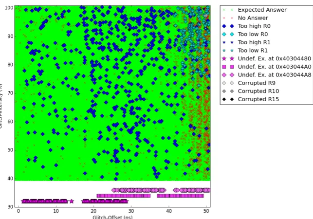
8.4 Storesled
Figure8.12 shows a whole surface testrun performed on the storesled. Faults for half of the registers were observed in the time period of only the first 45 ns Glitch-Offset. The single location testrun in figure8.13reveals that each store instruction has precisely targetable, partially with other store instructions overlapping, parameter areas. There is a clear relation between a later used register in the program code and a timely later register corruption in the figure. The presence of a store instruction seems to correlate with a higher amount of Data Abort Instructions. Table8.3shows a higher amount of Data Abort Exceptions than e.g. the movsled, addsled and nopsled.
Table 8.3: The answers obtained while injecting faults into the storesled test program on a single location.
Occurrence rate Measurement result
38.2350 % Undefined Instruction Exception 34.3510 % Expected Answer
12.2340 % Abnormal Answer 10.2500 % Data Abort Exception
3.4210 % No Answer
Remaining % Other
8.4 Storesled 47
Figure 8.12: The surface explored while injecting into the storesled test program. Some registers have a specific glitchable region; for other registers the glitchable areas are distributed more evenly throughout the total glitchable area.
48 8 Exceptions
few registers. Some register have precisely targetable ranges, others have only varying single successful glitch parameters. The scarce results after 50 ns, might be due to the whole surface testrun being performed for up to 50 ns.
Figure 8.14: The parameter space explored while injecting into the storesled test program on a different location than figure8.13. The clear regions for registers and relation between later glitches and higher registers from figure8.13does not hold for Glitch-Offsets above 60 ns.
The relation between the LR values in Data Abort Exceptions and the Glitch-Offset shows a partial trend between lower instruction addresses (i.e. earlier store instructions and lower registers) and a earlier Glitch-Offset. This relation seems to vanish after the first 50 ns.
8.5 Branchsled 49
Figure 8.15: The exceptions of a testrun with the storesled test program and the Glitch-Offsets between 0 to 150 ns are plotted as yellow dots. The X-axis shows the Glitch-Offset waited after the trigger signal before the injection was performed. The Y-axis shows the LR address stored by the exception handler.
8.5 Branchsled
Figure8.16shows a whole surface testrun performed on the branchsled. Apart from exceptions and a few R15 corruptions no faults were observed (especially no usable glitches).
Because of the absence of any register corruptions, we conclude that glitching the branchsled is not producing any usable faults with our measurement setup and selection of parameters.
50 8 Exceptions
Figure 8.16: The surface area explored while injecting into the branchsled test program. Only exceptions and a few R15 corruptions occurred.
8.6 Comparesled
Figure8.17shows the whole surface scan for the branchsled test program. We derived the most sensitive location (177104 motor steps in x direction and 302021 motor steps in y direction) for abnormal answers for the single location testrun in figure8.18.
Table8.4shows the overall distribution of answers for the single location testrun. Two abnormal answers were observed. One form of abnormal answer contains the unchanged initial R0 as the result, which could mean that the compare and branch combination being glitched into a branching state. The second form of abnormal answer contains the still initial R0 and R1 values, which should normally be modified.
Table 8.4: The answers obtained while injecting faults into the comparesled test program on a single location.
Occurrence rate Measurement result
71.5409 % Expected Answer
23.2388 % Undefined Instruction Exception 2.4756 % No Answer
0.9984 % Software Interrupt Exception 0.5649 % Abnormal Answer initial R0
0.4110 % Abnormal Answer initial R0 and R1 Remaining % Other
8.6 Comparesled 51
Figure 8.17: The surface explored while injecting into the comparesled test program. We observed exceptions, a few R15 corruptions, as well as several glitches, which returned the unchanged initial values for R0 or for R0 and R1 as result.
CHAPTER
9
Summary, Conclusion and Future Work
In this thesis we presented and evaluated techniques for exploring glitch effects on a 32-bit high speed embedded device microprocessor’s instruction execution. Chapter1 and2introduced our research question and EMFI. Chapter3listed the different techniques, which can be used for observing faults caused by FI in state-of-the-art embedded device processors. We thereby provide researchers and security analysts with a list of techniques to choose from for their own experiments. From this list we selected several techniques to evaluate in experiments.
Chapter4and5introduced our measurement setup, target and the test programs. We presented several test programs with the intention to observe faults on specific instructions or groups of instructions.
Chapter 6showed that faults are injectable into our target and that there are distinct chip surface areas, with high glitch sensitivity.
We introduced several test programs. Each test program was developed to cover one or more types of instructions. Experiments in chapter8showed that these test programs indeed show different fault behavior. The results give indications to which faults an instruction can be glitched. An attacker can use our provided or similar test programs to find the possible faults in a generic target and use them for crafting an attack.
We then explored the potential of the three selected glitch effect observation techniques: reading out registers with software, exceptions and tracing.
We concluded in chapter 8 that reading out registers is highly valuable for observing glitch effects. It is a fast and easy implemented technique compared to tracing. We cannot deduce how exactly a glitch affected the instruction execution, but for an attacker knowing that register values can be modified or that instructions can be skipped , it is enough for an attack. By gradually narrowing down the parameter space, this technique enabled us to find faults occurring with above 50 % probability.
Bibliography 57
[RV13] Jasper van Woudenberg Rajesh VelegalatiRobert Van Spyk: ‘Electro
Mag-netic Fault Injection in Practice’. In (2013), vol. (cit. on p.2).
[Sch08] J. SchmidtandC. Herbst: ‘A Practical Fault Attack on Square and Multiply’.
InFault Diagnosis and Tolerance in Cryptography, 2008. FDTC ’08. 5th Workshop on. Aug. 2008: pp. 53–58 (cit. on p.1).
[Shi] Alexander Shishkin: etm2human decoder for trace data output by Embedded
Trace Macrocells. url: https : / / github . com / virtuoso / etm2human (visited on 04/23/2014) (cit. on pp.12,31).
[Sko05] Sergei P. Skorobogatov:Semi-invasive attacks – A new approach to hardware
security analysis. 2005 (cit. on pp.1,5,6).
[Spr13] Albert Spruyt: ‘Building fault models for microcontrollers’. InWorkshop on
Trust-worthy Manufacturing and Utilization of Secure Devices (TRUDEVICE), Co-located with IEEE European Test Symposium (ETS)(2013), vol. (cit. on pp.9,10).
[Ver11] I. Verbauwhede,D. Karaklajic, andJ. Schmidt: ‘The Fault Attack Jungle - A
Classification Model to Guide You’. InFault Diagnosis and Tolerance in Cryptography (FDTC), 2011 Workshop on. Sept. 2011: pp. 3–8 (cit. on p. 1).
[Wou11] Jasper G. J.vanWoudenberg,Marc F. Witteman, andFederico Menarini:
‘Practical Optical Fault Injection on Secure Microcontrollers.’ In FDTC. Ed. by
List of Tables
3.1 The common ARM exceptions with occurrence reason. Source: [Exc] . . . 11
4.1 The potential targets or target groups we considered for this thesis and whether they fulfill all basic criteria. . . 17
5.1 An example testrun results database for the addsled test program with five single measurements. Id 2 contains an abnormal value for R1, so might be a successful glitch. The glitch parameters are described in table6.1. . . 26 5.2 Approximate average speeds for single measurements for our measurement setup
and the addsled target program. Using tracing requires much more time, because the CCS API and OCD needs to be used. . . 26
6.1 The parameters configurable in our measurement setup. . . 27
8.1 The answers obtained while injecting faults into the nopsled testprogram on a single location. . . 38 8.2 The answers obtained while injecting faults into the nopsled testprogram on a
single location. . . 45 8.3 The answers obtained while injecting faults into the storesled test program on a
single location. . . 46 8.4 The answers obtained while injecting faults into the comparesled test program on
a single location. . . 50 8.5 The findings while injecting into the different test programs . . . 52
APPENDIX
A
Decapsulated Beaglebone Processor
Figure A.1: The silicon layer of the BBB processor. The metal removal process left several impurities.
This chapter presents a view into the decapsulated BBB processor, the Texas Instruments Sitara
68 A Decapsulated Beaglebone Processor
AM3358AZCZ100 [Ins]. Unfortunately due to our positioning setup, we cannot precisely tell where our setup injected faults successfully, because the chip images did not give us more than a rough impression of the chip layout. Therefore the decapsulation did not contribute to this thesis, but is still shown here for an interested reader.
Figure A.2: The processor package opened up. The first metal layer of the die is visible.
FigureA.2shows the opened BBB processor package. The first layer is a metal mesh. Figure A.3shows a rough approximation where the die is during our experiments. For our experiments the injection probe reference positions are created by eyesight above the corners of the package. This positioning approach is sufficient for our experiments, but not for telling where exactly the die was during our experiment. It seems that the largest amount of glitches was injected not above the die, but above the bonding wires. Potentiality in our experiments most of the glitches are produced by currents in the bonding wires, instead of by injecting directly into the die.
Figure A.3: Figure8.5with the approximate position of the die marked in red.
69
removal process left several marks and impurities. The rectangular brighter structures might be memory. In the top right corner we can see a separate logic unit, which might be the A8 processor.