Implementation and Characterization of High Slew Rate CMOS
Op-Amp
Dr. Priyesh P. Gandhi
General Manager, Prakruti Consultancy Services, Vadodara, Gujarat, India
ABSTRACT
Operational Amplifiers (Op-Amp) are one of the most widely used building blocks for analog and mixed-signal systems. They are employed from dc bias applications to high speed amplifiers and filters. Different architectures like Two-Stage Op-Amp and Folded Cascode Op-Amp are simulated with different characteristics like slew rate, offset voltage, gain. For improving the slew rate, few modifications are carried out by adding current replication branch and auxiliary circuits in Op-Amp.
Keywords : Operational Amplifiers (Op-Amp), Slew Rate, CMOS, Propagation delay, Offset Voltage, Power Dissipation.
I. INTRODUCTION
An Operational Amplifier is a high-gain direct-coupled amplifier that is remarkably used in feedback connections. The word Operational Amplifier evolved from original applications in analog computation where the circuits are used to perform various mathematical operations like summation, integration, subtraction & derivation. Due to the performance and economic advantages of available units, present applications extend far beyond from the original applications, modern Op-Amps are used as general purpose analog data-processing elements. [12] .
The range of Op-Amp usage began to expand toward the present spectrum of applications in the early
1960s because various manufacturers were
developing modular, solid-state circuits. As the improvement in processing and designs, the integrated circuit will invade more areas once considered exclusively the domain of the discrete design, and it is probable that the days of the
discrete-component circuit, except for specials with limited production requirements, are numbered.[13]
Figure 1. Circuit symbol of Op-Amp
An Operational Amplifier (Op-Amp) is an integrated circuit (IC) which operates as a voltage amplifier. It has a differential input. That mean, it has two inputs which are in opposite polarity. An Op-Amp has a very high gain and single output, which means that the output signal is a large amount than input signal. An Op-Amp is regularly represented in a circuit diagram as shown in figure 1.
The Operational Amplifiers are key fundamentals in analog processing systems. The Op-Amps are an integral part of many analog and mixed signal systems. As the demand for mixed mode integrated circuits and systems increases, the design of analog circuits such as Operational Amplifiers (Op-Amps) in
CMOS technology becomes more difficult.
Operational Amplifiers (Op-Amps) with moderate DC gains, high output swing, and rational open loop gain band width product (GBW) are usually implemented with two-stage configuration.
The characteristics or the properties of an ideal per unit of time. Slew rate is usually measured in the unity gain noninverting amplifier configuration.
SR=I/C ----(2)
Zero Input Offset Current: - The difference between the currents into the two input terminals with the output terminal held at zero.
Zero Output Offset: - Output voltage when both inputs are grounded. For the ideal Op-Amp this offset has a 0 value.
Infinite Common Mode Rejection Ratio: - In an ideal Op-Amp, the output signal because of the common mode input voltage is zero, but it is nonzero in a practical device. The common mode rejection ratio
(CMRR) is the measure of the device's ability to
Zero Output Impedance: - Ideal Op-Amp behaves as perfect internal voltage source with no output impedance. This means the internal resistance is in series with the load. This results in a decrease in the output voltage of the load.
Input Offset Voltage: - The dc voltage that must be applied at the input terminal to force the quiescent dc output voltage to zero or other level, if specified, given that the input signal voltage is zero. The output of an ideal Op-Amp is zero when there is no input signal applied.
Infinite Bandwidth: - The input signal can be amplified with even infinitely large frequencies for ideal Op-Amp.
Infinite Input Impedance; - The input impedance is described as
Zin = Vin/Iin ---(4)
For ideal Op-Amps Zin is infinite. This means that Iin
is 0 (No current flows into the inputs of the Op-Amp) [13].
A CMOS Op-Amp needs very low supply currents,
less than 10μA and can operate with a supply voltage
II. Existing Architectures of Op-Amp
A typical circuit configuration of an un buffered Two-Stage Op-Amp (including the Input Differential Amplifier and the Second Gain Circuit) is shown in Fig.2. Transistors M1, M2, M3, and M4 form the first stage of the Op-Amp which generates the differential amplifier with differential to single ended transformation. In this stage, by using current mirror(M3 and M4) the conversion from differential to single ended is achieved. The current from M1 is stage. M6 is the driver while M7 acts as the load. For lower the gain at high frequencies and provide the compensation of the Op-Amp Capacitor Cc is used. The first stage and the second stage circuits use the same reference current; therefore, the bias currents in the two stages are controlled together [13]
Figure 2. Two Stage Op-Amp
The Folded-Cascode topology is as shown in Fig. 3. By its cascaded output stage, the swing of this design is constrained. Though only is needed to saturate the bottom most load transistors and the top-most current source transistors, in order to allow for process variations, a small safety margin is frequently
added to ensure saturation [1]. Accounting for these, and the required athwart the cascade devices, the differential output swing is with a voltage margin of 100 mV, this is estimated to be 2 V.
Figure 3. Folded Cascode Amplifier
reduced without affecting the slew rate. A fast CMFB, however, compromises the differential
frequency response. Characteristically, the
differential frequency response is optimized at the cost of slower common mode feedback. So, it becomes necessary to have the output stage current equal to that of the input stage.
A Telescopic Cascode Op-Amp, as shown in Fig.4, typically has higher frequency capability and consumes less power than other topologies of Op-Amp. Its high-frequency response stems from the fact that its second pole equivalent to the source nodes of the -channel cascade devices is determined by the trans-conductance of - channel devices as opposed to - channel devices, as in the Folded Cascode Op-Amp. Also, the parasitic capacitance at this node arises from only two transistors instead of three. The single stage
architecture naturally suggests low power
consumption. The disadvantage of a Telescopic Op-Amp is it has a severely limited output swing. The tail transistor directly cuts into the output swing from both sides of the output, so it is smaller than that of the Folded Cascode [1].
Figure 4. Telescopic Cascade Op-Amp
In the Telescopic Op-Amp all transistors are biased in the saturation region as shown in fig. 4. Transistors M1–M2, M7–M8, and the tail current source M9 must have at least to offer good common-mode
rejection ratio (CMRR), frequency response, and gain. The maximum differential output swing of a Telescopic Op-Amp is shown to be under identical conditions as before, the output swing of this design can be shown to be limited to in a 3-V supply system, this shows a 45% reduction of the available output swing
2.1 Modified CMOS Op-Amp
2.2 Two Stage CMOS Op-Amp
Figure 5. Schematic of Two Stage Operational Amplifier
As shown in fig.5 the given schematic for the
two stage Op-Amp. Differential input is M4 and
M5, which is the input of the first gain stage. Ib1
for the biasing current for the differential input
M4 and M5. This bias current is provided by M5,
which acts as a DC current source. M2 and
M3are a current mirror that acts as the active
load for input transistor.
directly connected to the DC supply voltage
VDD and hence no signal component. Transistor
M7 is the active load of transistor M6.
2.3 Folded Cascode Op-Amp
Figure 6. Schematic of Folded Cascode Op-Amp
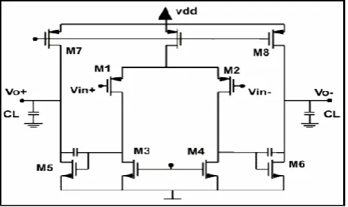
Fig.6 shows schematic of folded cascode Op-Amp. Differential inputs are applied at transistors M1and M2. Ibais is applied for the biasing at the input stge. Transistor M3 & M4 are the current mirror which acts as a resistive load for the input transistors. Transistors M8 & M9 are the cascading transistors. Here both M9 & M8 are the biasing transistors which boost the output of Op-Amp. Due to the cascading transistors the gain of the Op-Amp is enhanced. M6 and M7 are the output transistors. Here M7 is work as a active load for the M6.
2.4 Op-Amp using Current Replication Branch
The schematic of Op-Amp using current replication branch is as shown in fig.7. In the fig. transistor M1 & M2 are work as a current replication branch. Here the output transistor M11 can be transformed into an active M2. This transfers current variations Ia in M1-M2 to the output transistor M11 and increases the maximum positive output current by 2IB . Here the transistors M3-M7 generates adaptive loads which
exploit the large variation of output resistance of transistors M3 & M6 between triode and saturation regions. Bias voltage VbR sets these transistors at the boundary between triode and saturation regions in quiescent conditions. With both schemes, a current increase in Ia or Ib causes transistors M3 or M6 to go in triode mode and to develop large drain-source voltages. These changes cause large variations at nodes a and b, which lead to large currents in the output transistors M10 and, thanks to the current replication branch, M11.
Figure 7. Schematic of Op-Amp using Current Replicating Branch
2.5 Op-Amp using Auxiliary Circuit
Fig.8 shows schematic highlights auxiliary circuit that is added to the main circuit that connects output to the positive input. At the beginning of positive slew, the positive input has reached to its maximum value and output voltage is still at its minimum. Thus, M11 is ON and the current generated by this transistor will be mirrored by M12 and M13 and will be drawn from the differential pair of M1, M2. Transistor M11 remains ON until the output voltage reaches to a level that the difference between its
value and positive input is less than M11’s threshold
voltage (VT). After this point, the auxiliary circuit
will be in the OFF mode until the next positive slew and would not dissipate power. A precise design is required so that the main portion of output slew is done during the time that M11 is ON, otherwise, at first, we will have a fast increase in output waveform and after reaching to about 70 % of maximum voltage, M13 will be OFF and a decrease on output voltage will be observed, followed by a slow increment which will result in no or negligible SRE.
III.Simulation Result
3.1 Simulation Results of Two Stage CMOS Op-Amp
Figure 9. Transient Analysis of Two Stage Op-Amp in 180nm Technology
Figure 10. Slew Rate of Two Stage Op-Amp in 180nm Technology
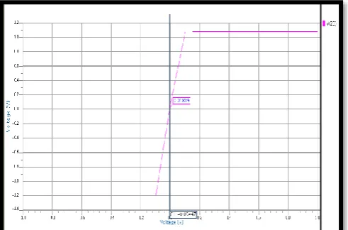
Figure 11. Offset Voltage of Two Stage Op-Amp in 180nm Technology
Figure 13. Transient Analysis of Two Stage Op-Amp in 90nm Technology
Figure 14. Slew-Rate of Two Stage Op-Amp in 90nm Technology
Figure 15. Offset Voltage of Two Stage Op-Amp in 90nm Technology
Figure 16. Frequency Response of Two Stage Op-Amp in 90nm Technology
3.2 Simulation Results of Folded Cascode Op-Amp
Figure 18. Slew Rate of Folded Cascode Op-Amp in 180nm Technology
Figure 19. Offset Voltage of Folded Cascode Op-Amp in 180nm Technology
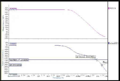
Figure 20. Frequency Response of Folded Cascode Op-Amp in 180nm Technology
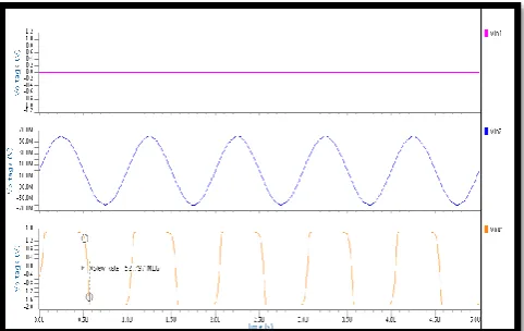
Figure 21. Transient Analysis of Folded Cascode Op-Amp in 90nm Technology
Figure 22. Slew Rate of Folded Cascode Op-Amp in 90nm Technology
Figure 24. Frequency Response of Folded Cascode Op-Amp in 90nm Technology
3.3 Simulation Results of Op-Amp using Current Replication Branch
Figure 25. Transient Analysis Op-Amp using Current Replication Branch in 180nm Technology
Figure 26. Slew Rate Op-Amp using Current Replication Branch in 180nm Technology
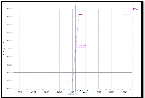
Figure 27. Offset Voltage Op-Amp using Current Replication Branch in 180nm Technology
Figure 28. Frequency Response Op-Amp using Current Replication Branch in 180nm Technology
Figure 30. Slew Rate Op-Amp using Current Replication Branch in 90nm Technology
Figure 31. Offset Voltage Op-Amp using Current Replication Branch in 90nm Technology
Figure 32. Frequency Response Op-Amp using Current Replication Branch in 90nm Technology
3.4 Simulation Results of Op-Amp using Auxiliary Circuit
Figure 33. Transient Analysis of Op-Amp using Auxiliary Circuit in 180nm Technology
Figure 34. Slew Rate of Op-Amp using Auxiliary Circuit in 180nm Technology
Figure 36. Frequency Response of Op-Amp using Auxiliary Circuit in 180nm Technology
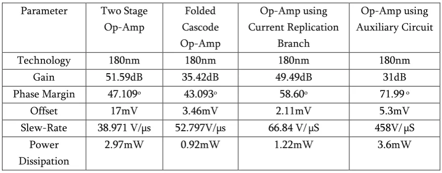
Table 1 and Table 2 shows the comparative result analysis for various architectures of Op-Amps.
IV. CONCLUSION
This paper showcase the implementation of high slew rate and low offset Operational Amplifier. Two stage Op-Amp, Folded cascade Op-Amp, Op-Amp using current replication branch & Op-Amp with addition of auxiliary circuits are simulated in TSMC 0.18 digital CMOS process and in generic 90nm technology. The various architectures and their simulation results will allow designers to fully explore the trade-offs in design of Op-Amps.
V. REFERENCES
[1]. Amana Yadav, "A review paper on design and synthesis of two stage CMOS Op-Amp", ISSN: 2231-196, ©IJAET, International Journal of Advances in Engineering & Technology, Jan 2012.
[2]. P.K.Sinha, Abhishek Vikram, Dr. K.S.Yadav, "Design Of Two Stage CMOS Op-Amp With
Low Power And High Slew Rate.",
International Journal of Engineering Research & Technology (IJERT) Vol. 1 Issue 8, October –
2012 ISSN: 2278-0181.
[3]. Priyanka Kakoty, "Design of a high frequency low voltage CMOS Operational Amplifier", International Journal of VLSI design & Communication Systems (VLSICS) Vol.2, No.1, March 2011.
[4]. Liang Zuo, Syed K. Islam, "Low-Voltage Bulk-Driven Operational Amplifier With Improved Transconductance", IEEE Transactions on Circuits And Systems—I: Regular Papers, Vol. 60, NO. 8, August 2013.
[5]. Ehsan Kargaran , Hojat Khosrowjerdi , Karim Ghaffarzadegan, "A 1.5 V High Swing Ultra-Low-Power Two Stage CMOS Op-Amp in 0.18 um Technology", 2010 2nd International Conference on Mechanical and Electronics Engineering (ICMEE 2010).
[6]. Aguado-Ruiz, Antonio Lopez-Martin, Javier Lopez-Lemus, and Jaime Ramirez-Angulo, "Power Efficient Class AB Op-AmpsWith High and Symmetrical Slew Rate", IEEE Transactions on Very Large Scale Integration (VLSI) Systems, Vol. 22, No. 4, April 2014.
[7]. Fermin Esparza-Alfaro, Salvatore Pennisi, Gaetano Palumbo, Fellow, Antonio J. Lopez-Martin, "Low-Power Class-AB CMOS Voltage Feedback Current Operational Amplifier WithTunable Gain and Bandwidth", IEEE Transactions on Circuits And Systems—Ii: Express Briefs, Vol. 61, No. 8, August 2014. [8]. Rahul Singh, Yves Audet, Yves Gagnon, Yvon
Sava, Étienne Boulais, and Michel Meunier "A Laser-Trimmed Rail-to-Rail Precision CMOS Operational Amplifier", IEEE Transactions On Circuits And Systems—Ii: Express Briefs, Vol. 58, No. 2, February 2011.
[9]. Rosario Merlino, Graziella Scandurra, and Carmine Ciofi, Member, IEEE, "A Very Low Offset Preamplifier for Voltage Measurements
in the μV Range", IEEE Transactions on
[10]. Shi Bu, Ka Nang Leun, "A 116-dB CMOS Op Amp with Repetitive Gain Boosting and Sub-threshold Operation", IEEE Transactions on Circuits And Systems—I: Regular Papers, Vol. 60, No. 8, August 2006
[11]. Hossein Kassiri B and M. Jamal Dee. "Slew-Rate Enhancement for a Single- Ended Low- Power Two-Stage Amplifier" 978-1-4673-5762-3/13/$31.00 ©2013 IEEE
[12]. http://services.eng.uts.edu.au/~venkat/dads/add notes.pdf
[13]. Phillip E. Allen, Douglas R. Holberg, "CMOS Analog Circuit Design", Oxford University Press, Second Edition, 2002, pp.439-488.
[14]. Harry W. Li, R. Jacob Baker and David E. Boyce, CMOS Circuit Design, Layout and
Simulation, IEEE Press Series on
Microelectronics Systems, 2005.
Table 1. Comparative Analysis of Simulation Results in 90nm
Parameter Two Stage
Table 2. Comparative Analysis of Simulation Results in 180nm
Parameter Two Stage
Technology 180nm 180nm 180nm 180nm
Gain 51.59dB 35.42dB 49.49dB 31dB International Journal of Scientific Research in Computer Science, Engineering and Information Technology (IJSRCSEIT), ISSN : 2456-3307, Volume 5 Issue 1, pp. 574-585, January-February 2019.