Scholarship at UWindsor
Scholarship at UWindsor
Electronic Theses and Dissertations
Theses, Dissertations, and Major Papers
1-1-2007
A MEMS non-planar ultrasonic microarray.
A MEMS non-planar ultrasonic microarray.
Matthew Meloche
University of Windsor
Follow this and additional works at:
https://scholar.uwindsor.ca/etd
Recommended Citation
Recommended Citation
Meloche, Matthew, "A MEMS non-planar ultrasonic microarray." (2007). Electronic Theses and
Dissertations. 7027.
https://scholar.uwindsor.ca/etd/7027
by
M a tth e w M elo ch e
A Thesis
Subm itted to the Faculty of G raduate Studies
through Electrical and Computer Engineering
in P artial Fulfillment of the Requirements
for the Degree of M asters of Applied Science
a t the University of W indsor
Archives Canada
Archives Canada
Published Heritage
Branch
3 9 5 W ellin g to n S tre e t O tta w a O N K 1 A 0 N 4 C a n a d a
Your file Votre reference ISBN: 978-0-494-35054-6 Our file Notre reference ISBN: 978-0-494-35054-6
Direction du
Patrimoine de I'edition
3 9 5 , rue W ellin g to n O tta w a O N K 1 A 0 N 4 C a n a d a
NOTICE:
The author has granted a non
exclusive license allowing Library
and Archives Canada to reproduce,
publish, archive, preserve, conserve,
communicate to the public by
telecommunication or on the Internet,
loan, distribute and sell theses
worldwide, for commercial or non
commercial purposes, in microform,
paper, electronic and/or any other
formats.
AVIS:
L'auteur a accorde une licence non exclusive
permettant a la Bibliotheque et Archives
Canada de reproduire, publier, archiver,
sauvegarder, conserver, transmettre au public
par telecommunication ou par I'lnternet, preter,
distribuer et vendre des theses partout dans
le monde, a des fins commerciales ou autres,
sur support microforme, papier, electronique
et/ou autres formats.
The author retains copyright
ownership and moral rights in
this thesis. Neither the thesis
nor substantial extracts from it
may be printed or otherwise
reproduced without the author's
permission.
L'auteur conserve la propriete du droit d'auteur
et des droits moraux qui protege cette these.
Ni la these ni des extraits substantiels de
celle-ci ne doivent etre imprimes ou autrement
reproduits sans son autorisation.
In compliance with the Canadian
Privacy Act some supporting
forms may have been removed
from this thesis.
While these forms may be included
in the document page count,
Conformement a la loi canadienne
sur la protection de la vie privee,
quelques formulaires secondaires
ont ete enleves de cette these.
A novel discretized hyperbolic paraboloid geometry ultrasonic sensor m icroarray of capacitive type sensors has been developed to intrinsically provide a broadband constant beam width beamforming capability w ithout any microelectronic signal processing. A m athem atical model has been
developed and verified to characterize the array response. A design methodology has been presented th a t enables the determ ination of array dimensions, sensor type, device modeling and behavioral analysis in a straight-forward manner. The developed theory has been used to design two ultrasonic sensor microarrays: one in the 2.3 MHz - 5.2MHz frequency regime and another in the 113 kHz-167 kHz frequency regime. Individual capacitive type sensor elements have been designed using a cross-verification method th a t involves lumped element modeling, 3-D
First, a large thank-you to my advisor Dr. Sazzadur Chowdhury, w ithout his help this project would not have come to completion.
Thank-you also to Ashkan Hoseinzadeh and Tara Droullaird for assistance w ith editting. Andrew Tam, This was your idea. Thank-you.
A b stra ct iv
D ed ic a tio n v
A ck n ow led gm en ts vi
List o f F igu res x
List o f Tables xii
1 In tro d u ctio n 1
1.1 Goals ... 1
1.1.1 B a c k g ro u n d ... 1
1.1.2 Research G o a l s ... 6
1.2 Target Applications ... 7
1.3 Historical C o n t e x t ... 8
1.4 Overview of MEMS Fabrication T e c h n iq u e s ... 10
1.4.1 Spin C o a t i n g ... 10
1.4.2 Optical L ith o g ra p h y ... 11
1.4.3 S p u tte rin g ... 14
1.4.4 Deep Reactive Ion Etching ... 15
1.5 Packaging Techniques ... 16
1.5.1 Adhesive B o n d i n g ... 16
1.5.2 W ir e b o n d in g ... 16
1.6 Fabrication M ethodologies... 17
1.6.2 Hand Assembly for Low Volume, Low Complexity Structures ... 21
1.7 Physical Application R e q u ire m e n ts... 22
1.8 Specific Research O b jectiv es... 23
1.9 Principle R e s u l t s ... 24
1.10 Organization of T h e s is ... 25
2 N o n -P la n a r B eam form in g 26 2.1 Theory of Hyperbolic Paraboloid Geometry Acoustical T r a n s d u c e r ... 26
3 A rray D e sig n 36 3.1 Determ ination of Array S id e le n g th ... 36
3.2 Determining the Number of Sensing S u r f a c e s ... 37
3.3 Array Height and Tier Elevation C a lc u la tio n s... 38
3.3.1 Tier Elevation ... 40
3.4 Step 4 - Sensing Surface D esig n ... 42
3.5 Numerical E x am p le... 42
3.5.1 Problem D efin itio n ... 42
3.5.2 S o lu tio n ... 43
3.6 Array Design for I A V S S ... 47
3.6.1 Problem D e fin itio n ... 47
3.6.2 S o lu tio n ... 48
4 T ransducer M o d e lin g 53 4.1 MEMS Acoustic S e n s o rs ... 53
4.1.1 Piezoelectric T ran sd u ctio n ... 53
4.1.2 Piezoresistive T r a n s d u c tio n ... 54
4.1.3 Capacitive T ra n sd u c tio n ... 55
4.2 Modeling L evels... 56
4.3 Lumped Element M o d e l i n g ... 57
4.3.1 Reliability S t u d y ... 62
4.3.2 Lumped Element R e s u l t s ... 67
4.4 Finite Element A n a ly s is ... 69
4.4.1 Resonant F r e q u e n c y ... 69
4.4.3 Capacitance Change Over A ctuation R a n g e ... 70
4.4.4 Maximum D isp la c e m e n t... 71
5 F abrication 73 5.1 Array Fabrication D e t a i l s ... 73
5.1.1 Stage 1: Wafer P r e p a r a tio n ... 74
5.1.2 Stage 2: PVD M etal Deposition ... 74
5.1.3 Stage 3: L ith o g rap h y ... 75
5.1.4 Stage 4: M etal Etching ... 76
5.1.5 Stage 5: Silicon E t c h ... 76
5.1.6 Stage 6: Photoresist S t r i p ... 78
5.1.7 Stage 7: Buffered Oxide Etch Diaphragm R elease... 78
5.1.8 Stage 8: Array Assembly ... 80
5.2 Packaging D e ta ils ... 81
6 C on clu sion s 84 R eferen ces 87 A M atlab C od e 91 A .l Elevations Vs. Number of sensing surfaces per a x i s ... 92
A.2 Lumped Element Simulation ... 94
A.2.1 Numerical Example ... 94
A.2.2 Array Design S im u latio n ... 96
A.2.3 Support F u n c tio n s ... 98
A.3 Mainlobe -3dB Cross-Section G en e ra tio n ... 103
A.3.1 Support F u n c tio n s ... 106
A.4 Accuracy of Summation Vs. Integral f o r m ... 106
A.4.1 Support F u n c tio n s ... 108
A.5 Generation of Polar P l o t s ... 109
A.5.1 Support F u n c tio n s ... 110
1.1 Schematic of Constant Beamwidtli Array Based on Synthesis T h e o r y ... 5
1.2 Block Diagram of the Integrated Active Vehicle Safety System (IAVSS) ... 7
1.3 Safety S h e l l ... 8
1.4 Application of a Photoresist by S p in n in g ... 12
1.5 Optical Lithography M a c h in e ... 13
1.6 Ion Beam Sputtering ... 15
1.7 Embedded Mask Method: Phase 1 - Mask D e p o s itio n ... 19
1.8 Embedded Mask method: Phase 2 - P attern Transfer to W a f e r ... 20
1.9 Main Steps to Create a Hand Assembled A r r a y ... 21
2.1 Hyperbolic Paraboloid Shaped S u rfa c e ... 28
2.2 Beamforming w ith the Continuous Aperture S e n so r... 29
2.3 Seven Elevation Discrete Hyperbolic P a ra b o lo id ... 31
2.4 From Continuous Aperture Transducer to Discrete A r r a y ... 31
2.5 Main Beam -3dB Cross-Sections of Continuous and Discrete A rra y s... 33
2.6 W orst Case Passband Approximation E r r o r ... 34
2.7 3-D Change in Beamshape over Change in L a m b d a ... 34
2.8 Cross-Sectional Changes in Beamshape Over Change in L a m b d a ... 35
3.1 Number of Sensing Surfaces Vs. Sidelobe I n t e n s i t y ... 38
3.2 Array Height and Out-of-Plane Twist ... 39
3.3 Discrete Array Height S am pling ... 39
3.4 Number of Sensing Surfaces Vs. Total H e i g h t... 40
3.5 Number of Elevations Vs. Number of Sensing S u rfa c e s ... 41
3.7 Array Beamshape at 2.3 M H z ... 45
3.8 Array Beamshape at 3.75 M H z ... 45
3.9 Array Beamshape at 5.2 M H z ... 46
3.10 Array Mainlobe Cross-Sections at -3 d B ... 46
3.11 Illustration of IAVSS Array and Geometry A p p ro x im atio n ... 50
3.12 IAVSS Array Beamshape a t 113 k H z ... 50
3.13 IAVSS Array Beamshape a t 140 k H z ... 51
3.14 IAVSS Array Beamshape at 167 k H z ... 51
3.15 IAVSS Array Mainlobe Cross-Sections a t -3 d B ... 52
4.1 Piezoelectric A c t u a t o r ... 54
4.2 A Schematic View of a Capacitive S e n s o r ... 56
4.3 Array Modeling Details: Beamforining Array - Transducer - D ia p h r a g m ... 58
4.4 Equivalent Circuit M o d e l ... 59
4.5 Maximum Shear Stress Theory - Safe Area for in Plane Stress ... 63
4.6 O ctahedral Shear Stress Theory - Safe Area for in Plane S t r e s s ... 65
4.7 Coulomb-Mohr C riteria - Safe Area for Plane S t r e s s ... 66
4.8 Finite Element Pull-In Voltage Prediction using I n te lliS u ite ... 71
4.9 Maximum D isp la c e m e n t... 72
5.1 Fabrication M aterial L e g e n d ... 74
5.2 Stage 1 Fabrication Details... 75
5.3 Stage 2 Fabrication Details... 75
5.4 Stage 3 Fabrication D etails... 76
5.5 Stage 4 Fabrication D etails... 77
5.6 Stage 5 Fabrication D etails... 77
5.7 Stage 6 Fabrication D etails... 78
5.8 Stage...7 Fabrication D etails... 79
5.9 Stage...8 Fabrication Details... 80
5.10 W irebonding Bonding D ia g r a m ... 82
1.1 Common W irebonding P r o c e s s e s ... 17
1.2 Maximum Ultrasound Exposure Levels by Frequency ... 23
3.1 Beamwidth Control Param eter K Values ... 37
3.2 Numerical Example - Results ... 44
3.3 IAVSS Array Design Performance Specifications ... 47
3.4 IAVSS Array G e o m e t r y ... 49
4.1 Gauge Factors for Differing M aterials ... 55
4.2 3 x 3 Array Diaphragm Design S p e c ific a tio n s... 67
4.3 Lumped Element Modeling Results For 3 x 3 Array ... 68
4.4 29 x 29 Array Diaphragm Design P a r a m e te r s ... 68
4.5 Lumped Element Modeling Results For 29 x 29 A r r a y ... 69
4.6 Lumped Element Modeling Results For 29 x 29 A r r a y ... 70
4.7 Capacitance Change A n a ly s is ... 70
5.1 W irebonding Diagram Details ... 82
5.2 Die Details ... 83
In tro d u ctio n
1.1
Goals
1.1.1
B ack grou n d
Frequency independent broadband acoustical beamforming using a MEMS-based ultrasonic sensor microarray th a t can provide a real-time variable directional sensitivity w ithout microelectronic sig nal processing can overcome the current limitations associated with ultrasonic ranging, acoustical imaging, etc [1, 2], In typical one-dimensional or two-dimensional beamforming techniques, arrays of acoustical sensors are used to enhance the acoustical signals coming from a desired direction whereas the signals coming from the other directions are destructively cancelled out. Different beamforming algorithms, such as delay-and-sum, filter-and-sum or FFT-based techniques implemented in micro electronic based signal processing circuitry are used for this purpose. These algorithms differ in complexity, processing time, and real-time implementation issues [3, 4, 5].
replaces the fixed time delay between array elements w ith phase shifting filters. The phase shifting filters are typically set up to be inversely proportional to frequency. This makes the effective array length a constant multiple of the wavelength, thus yielding a constant response over a wide range of frequencies. Filter and sum beamformers provide additional capability a t the cost of vastly more complex implementations th an simple delay and sum beamforming techniques.
Due to their superior properties, the bulk of broadband beamforming research effort has been focused on filter and sum beamformers. Combined with digital signal processing, this provides a robust and flexible solution to the need for broadband beamforming. An example of this type of beamforming is the technique detailed in [6], in which several acoustic arrays are overlaid. This allows the relation between the number of transducers and frequency range to be logarithmically related. This technique, known as harmonic nesting, uses bandpass filters so th a t each subarray contributes only in its optim al frequency range. Here each subarray uses a finite impulse response (FIR) based filter and sum beamformer. This solution is limited as a discrete set of transducers cannot exactly implement a continuous range of aperture sizes. Also design of the elemental filters for each sensor element of each subarray is a challenging problem. This solution and its variants require significant processing power to be implemented, adding to system cost, complexity and power requirements.
The time delay associated w ith intensive processing requirements limits the use of such beam formers in applications where real-time implementation issues are crucial. An example of one of these applications is proximity detection for automotive collision avoidance systems. In [7], it has been determined th a t ultrasonic sensors can be p art of an integrated autom otive collision avoidance system along w ith other sensing schemes, such as radar, laser, and vision-based proximity detection systems.
In the recent years, significant progress has been made in the design of MEMS-based acoustical sensor microarrays, bo th in the audio frequency and ultrasonic domain [9, 10, 11, 12]. A planar, uniformly spaced MEMS acoustical sensor inicroarray is presented in [13]. In this design the array features rear-vented capacitive elements to attain high sensitivities in the audio frequency range. This 3 x 3 array targets hearing aid instrum ents as an application and has an operating frequency range of 350 Hz - 18.0 kHz. Each square sensor element has a side length of 1.2 mm and a sensitivity of 10.2 m V /pa. The array uses polysilicon-germanium (Poly-SiGe) for a diaphragm m aterial to enhance sensitivity.
Curved arrays have been well accepted into the medical diagnostic field. Approximately half of all diagnostic ultrasound heads are curvilinear [14, 15]. A commercially produced curvilinear MEMS-based ultrasonic array is presented in [14] which uses a 128 element convex geometry array. The substrate is thinned to 150/xm through chemical etching and mechanical abrasion. This thinned wafer is flexible enough to be mounted to a fixed backplate which maintains the radius of curvature desired for the head. It has been shown experimentally th a t the effects of this substrate bending do not significantly affect the performance of the transducer array. The curvilinear sensor array has a center frequency of 4.0MHz and a bandw idth of 125% . Fabrication challenges abound for these arrays however. Extreme care is needed to model the stress in the silicon substrate during bending. Fabrication param eters must also be tightly controlled to ensure th a t residual stresses and film quality is consistent. Care is needed during handling and assembly to ensure th a t localized stresses do not cause the device to fracture. In addition, the tolerances on the backplate used to hold the array shape must be manufactured to within 0.01mm of the desired radius of curvature. Also, the offset between the transducer and the plastic nose piece is adjusted to w ithin 7.5/tm [14]. The high performance of these devices shows th a t the technology is able to deliver excellent results, although this m ethod of generating a convex surface is highly challenging, causing reduced yields, and increased pricing. These arrays feature a good bandwidth, but still require an external beamforming engine to produce a coherent beam.
Peizocomposite based curved arrays are available as a competing technology. Advances in piezo electric m aterials have m aintained this technology as m ainstay in ultrasonic transducers [17].
Frequency independent constant beamwidth beamforming (FICBB) capability is highly desirable in directional speech acquisition, sonar, acoustical ranging, automotive proximity detection systems, acoustical imaging, and many other applications [6].
Only a few algorithms are available in the literature th a t can be used to provide a frequency independent constant beamwidth with a planar array geometry; however, they seem to be com putationally expensive while real-time implementation is a concern. Additionally, it appears th a t integration and packaging of the sensor m icroarray w ith additional microelectronic circuitry neces sary for FICBB is challenging in term s of extra die space and low-loss interconnection paths. Thus, there exists a need to investigate other techniques th a t could be used to minimize related circuitry. One of them is exploiting the geometrical properties of a surface th a t can intrinsically enable a beamforming capability.
It has been established th a t a continuous aperture hyperbolic paraboloid shaped transducer ex hibits an intrinsic property of constant beam width frequency independent beamforming [18, 19]. The design was realized in macroscale and experimental results were presented. However, obtaining an accurate curvature requires very tight tolerances during the manufacturing process. More critically, maintaining a constant air gap over a curved surface proved to be a formidable challenge.
The state-of-the-art micro-fabrication technology is able to support micrometer scale tolerances and also can m aintain uniform air gaps. However, micro-fabrication is a planar process and cur rent micro-fabrication techniques are not suitable to realize curved surfaces such as a hyperbolic paraboloid. Investigation shows th a t this issue could be resolved by fabricating a tiered geometry using planar process steps th a t can approxim ate a discretized hyperbolic paraboloid surface. This is highly desirable as long as the desired operating frequency range is w ithin the limit imposed by the geometric approximation.
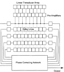
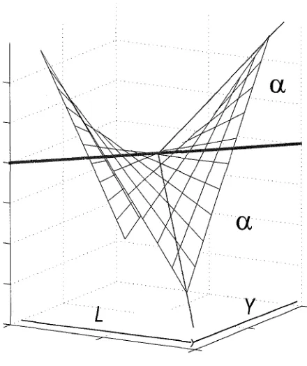
The basic concept of intrinsic beamforming finds its root on two independent lines of thinking. One of them is the synthesis m ethod and the other is based on the ray theory. The synthesis method is shown graphically in Figure 1.1.
S ' l T l i X )
In this method a number of basic ---- -— patterns which have been displaced using delay lines x
are superimposed in space. The centers of the superimposed beam patterns are displaced in space b y a n a m o u n t w h ic h in c r e a s e s lin e a r ly w i t h f r e q u e n c y in s u c h a w a y t h a t t h e a r r a y r e s p o n s e w id e n s
Linear Transducer Array
Pre-Amplifiers
Delay Lines
Phase Correcting Network
Output
we proceed from one end of the surface to the other, then the resulting surface in three dimensions would be a hyperbolic paraboloid. A constant beamwidth broadband beamformer can be achieved through this technique. An additional feature is th a t the geometry is symmetric along the axis of twist, as well as along the axis a t a right angle. The bandw idth ratio over which the array will operate is a function of the number of strips in the array [19, 20]. It appears th a t this characteristic can be exploited successfully to realize a discretized hyperbolic paraboloid surface w ith a desired bandwidth.
. The same array can be developed by using the ray theory. If it is required to have a beamwidth of 2a, which is independent of frequency, we can consider a linear strip array having a length much greater then the wavelength. This array will have a very narrow beamwidth in the direction normal to the array. By placing a series of strip arrays so th a t the direction of the nominal array normal gradually varies from —a to +a, a beamwidth of 2a could be achieved. If the angle of the twist is varied linearly as the surface proceeds along the axis of rotation, the resulting surface would be a linear twist.
Comparing the linear twist to the hyperbolic paraboloid, it has been shown th a t for the linear twist, the angle of deflection of a straight line on the surface is directly proportional to the distance traveled along the twist axis [19]. For the hyperbolic paraboloid, it is the tangent of the angle of deflection which increases linearly w ith distance travelled along the axis of twist. For angles less than 10° the tangent and its angle in radians are approximately equal. Therefore, for small angular twists, the two surfaces are identical and the complete beamshape could be calculated using the m athem atics for either geometry. The hyperbolic paraboloid is chosen as it is a doubly ruled quadratic surface and can be constructed entirely out of straight lines.
1.1.2
R esearch G oals
Sensor Subsystem
M E M S / Nano
Drive By
Head-Up Displ Acoustic Alar IAVSS
Safety S
Driver
Input
V
+ '
External Disturbance
Figure 1.2: Block Diagram of the Integrated Active Vehicle Safety System (IAVSS)
1.2
Target A pp lications
The developed sensor microarray could be used for high frequency ultrasonic imaging applications or as an enabling sensor system for the integrated active vehicle safety system (IAVSS) as proposed in [7]. The IAVSS system includes a MEMS sensor subsystem, a controller, Drive-by-Wire subsys tems, Vehicle network subsystem (TTCAN or FlexRay), and a Driver interface subsystem (head-up display/ acoustic alarm) as shown in Figure 1.2
External Disturbance
Driver Input Error
IAVSS Safety Shell
Figure 1.3: Safety Shell
The system is fundamentally different approach from other safety systems where the components work individually w ithout any central processor taking care of vehicle safety [7]. The system has the potential to enable safe autonomous driving in the future in almost any driving scenario. One m ajor challenge to implement IAVSS is the time delay associated w ith the implementation of the varied and complex algorithms as mentioned in National Highway Traffic Safety A dm inistration (NHTSA) Report to process sensor data, th reat level estim ation and decision making [21]. The challenge could be better addressed by minimizing the use of complex algorithms for signal processing. The current need for these expensive algorithms indicates an area in need of improvement through the elimination of the time delay associated w ith conventional ultrasonic beamformers. In order for the system to obtain maximum information for decision making, frequency independent broadband beamforming is necessary. The implementation of a beamforming engine is a processor intensive operation. In order to minimize the am ount of processing required, the sensing element should be able to provide this functionality intrinsically.
1.3
H istorical C ontext
submarines. This work was pioneered in the First World War due to the effectiveness of German submarines a t disrupting Atlantic trade [22]. Professor Paul Langevin used the piezoelectric effect to create the world’s first underwater ultrasonic transducer, a quartz crystal transducer operating at 50 kHz. Unfortunately, development of the transducer was not completed until after the First World War. It is interesting to note th a t the initial application for this device was depth metering.
During the Second World War, ultrasonic transducers were improved by the discovery of Ammo nium dihydride phosphate (ADP). ADP crystals proved to be far more suitable th a n the Rochelle salt piezoelectric crystals th a t had been used to this point. During this period, ultrasonic systems had m atured to be effective at finding submarines, as well as being m iniaturized enough to be mounted on torpedoes like the ’mine m ark 24’ [22], These torpedoes could be launched from a subm arine or airplane, and were capable of tracking a target as far away as 200 yards. Ultrasound detection and tracking proved to be a critical technology for defence against submarine based warfare. O ther applications stemming from research during World W ar II included moving target indicator radar, where static reflections were cancelled only showing moving targets. These systems were imple mented using ultrasonic delay lines to store previous scan data. 1924 saw R. W. Wood and A. L. Loomis examining the effects of high-intensity ultrasound. They were able to show m any striking ef fects produced by high intensity ultrasound, however they remained laboratory dem onstrations [22]. The second practical application of ultrasound technology was for defect detection in m aterials, an application th a t remains common today. This technology was developed independently during the Second World W ar in both America and Britain. During this period the first medical diagnostic applications were also developed; it was discovered th a t ultrasound could be used to detect cancer
[2 2].
During the 1940’s and 1950’s medical applications for ultrasound underwent slow development, but during the 1960’s it began to see increased clinical use, burgeoning and becoming a m ainstream diagnostic and therapeutic treatm ent during the 1970’s. Several paradigms of ultrasonic imaging are possible. A-Mode, ultrasound uses a simple time based display and allows for position measurement and dimensioning of the observed structures. B-Scan instrum ents couple an A-mode unit to a beam- scanning apparatus and an intensity m odulated display to produce a 2-D cross sectional image of the area under inspection. This is the most common form of diagnostic ultrasound today. Finally M- Mode ultrasound uses a standard A-Mode instrum ent w ith a modified display. This allows positional monitoring of moving structures such as artery walls and heart valves [23].
ensure removal of adhered contaminants. This technique is used in a wide range of applications; from cleaning jewellery to de-griming automotive parts to cleaning surgical implements. Ultrasonic waves can be used to detect voids in a m aterial [24]. This ability allows for non-destructive testing for m aterial or weld defects. Ultrasound is also able to detect changes in density. This allows the accurate measurement of coating thicknesses. Each layer can be characterized for thickness independently after all layers are deposited. This is used for quality control for automotive paint. It can also be frequently used to detect if a body panel has been repainted, as the thickness profiles will be notably different. The original application for ultrasound was ranging, and ultrasonic range sensing continues to see development. Ultrasonic range sensing allows accurate non-contact distance measurements. This sensing can be used in some applications where other non-contact sensing mechanisms such as laser cannot be used. For example level measurement in reservoirs of molten metal used for casting. Ultrasound continues to find new applications in industry, and the availability of MEMS ultrasonic sensing promises to ensure new applications continue to be found.
1.4
O verview o f M E M S Fabrication Techniques
MEMS fabrication began in the early 1960’s. The first commercial sensor fabricated by w hat is now considered MEMS techniques was produced by Honeywell in 1962 [25]. Micromachining techniques have been developing rapidly in recent years, and the variety of geometries th a t can be m anufactured continues to grow; as does the number of m aterials available. The m ajor techniques needed to fabri cate the developed discretized hyperbolic paraboloid acoustic sensor microarrays and the techniques needed for assembly of the IAVSS sensor microarray are outlined in the following sections.
1.4.1 Spin C o a tin g
Spin coating is a technique used to apply both tem porary materials such as photoresist, and perm a nent structural materials. Spinners are found in all microfabrication labs. The spinning process can be used to deposit viscous m aterials over wafers w ithout extreme topologies. Due to poor adhesion between photoresist and metals, PSG and polysilicon, wafers are typically ’prim ed’ w ith Hexamethyl disalazane (HMDS) before the application of a photoresist. A primed wafer features a hydrophobic surface, which ensures th a t surface moisture on the wafer will not interfere w ith photoresist adhesion.
is primed, resist is applied to the center of the wafer a t approximately 300 RPM (Figure 1.4.A). The spinner then rapidly accelerates to its final spin speed. This evenly spreads the resist across the wafer surface (Figure 1.4.B). Finally th e spinner m aintains the final spin speed for a short interval of time, typically around 1 minute (Figure 1.4.C) to allow the solvent in the resist to begin evaporating.
The main param eters for determining the thickness of the deposited film is viscosity, solvent evaporation rate and spin speed. A laboratory spinner is typically capable of speeds up to 10 000 RPM , w ith an accuracy of ±1 RPM. This level of control is necessary as a 50 RPM variation from the set point can result in as much as a 10% thickness variation. Typical resist thicknesses are in the range of 1/im, although this technique can be used to apply films w ith thicknesses between 0.1/rin and 500/rm. At a /xm thickness, spin application can obtain a film thickness uniformity of ±5nm across the wafer. Spin speed can be used to vary the film thickness over 1 decade (ie. from 1/xm to 10/xm); beyond this limit, a new resist formulation must be used [26, 27].
1.4.2
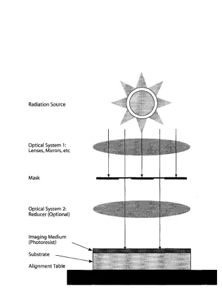
O p tical L ith ograp h y
Optical lithography is, in its essence, photography and consists of 4 m ajor steps: • Photosensitive film (photoresist) application
• Alignment of mask and wafer • Exposure of photoresist • Development of patterns
W afer
P h o to re s is t
V a c u u m C h u c k
A. Apply Photoresist
B. Rapid A c c e le ra tio n S p r e a d s Resist
C. Final Spin - 5 0 0 0 RPM
R adiation Source
O ptical System 1: Lenses, M irrors, e tc
Mask
O ptical System 2: R educer (O ptional)
Im aging M edium (P hotoresist)
S u b stra te
A lig n m en t Table
1.4.3
S p u tter in g
Sputtering is a commercially im portant technique for thin film deposition. This technique is used to apply films to computer disks, liquid crystal displays, compact discs and hard-drives for computers. It is also used to apply hard coatings to cutting tools, gears, and automotive parts [27]. Sputtering is a type of physical vapor deposition and as such m aterial is transferred directly from a source m aterial target to the wafer. During sputtering, the source m aterial target is charged to a high negative potential. It is then bombarded w ith positively charged ions from argon plasma. The target m aterial is ejected from the source mainly by momentum transfer from neutral atoms. Ejected surface atoms are deposited onto a substrate (the wafer) placed on the anode. In order to maximize the yield of the process, ion energies in the range of 500-3000 Volts are used. Due to the large ion energies present, the deposited m aterial is able to penetrate 1 or 2 atomic layers into the substrate, producing extremely strong adhesion. In order to sustain a DC plasma a relatively high pressure of 1 x 10⁻² Torr or greater is needed. At 10"1 Torr, the mean-free p ath of the sputtered ions is approximately 1mm. Because of the multiple collisions of the atom between release and arrival, the atoms arrive at random incidence angles. This leads to excellent step coverage compared to other physical vapor deposition techniques.
A relatively recent variation called ion beam sputtering provides both excellent adhesion and a high purity deposition. The operating pressure for this technique is approximately 1 x 10~4 Torr. In this layout, an ion beam as shown in Figure 1.6 w ith an energy in the hundreds to thousands of electron volts (eV) is directed a t the sputtering target. B oth reactive and inert gases can be used for ion beam sources. The substrate is suitably located as to be isolated from the plasm a generation source, this perm its independent control over the substrate tem perature, gas pressure and type of particle bom bardm ent of the growing film. It is also possible to control the energy and target current density independently. Limitations of this technique include a deposition rate th a t is lower th an traditional sputtering techniques and a relatively small deposition area.
p Ion Beam Substrate
Target
Figure 1.6: Ion Beam Sputtering
1.4.4
D e ep R ea ctiv e Ion E tch in g
Reactive ion etching (RIE) of silicon is a well-established tool for IC fabrication and has been indispensable since the early 1980’s. Deep Reactive Ion Etching (DRIE) is a specialized inductively- coupled-plasma reactive-ion-etch (ICP-RIE). DRIE overcomes several of the lim itations of traditional RIE by improving the etch rate, selectivity against photoresist and Si0 2 , and the maximum aspect
ratio. One of the common DRIE techniques is the Bosch DRIE. The Bosch process DRIE involves alternating between two stages. In the first stage, a thin fluorocarbon polymer film is deposited. This film acts as a protective layer for the sidewalls during the etch stage. The polymer is constructed of C F2 molecules deposited from a C4F8 gas source. The second stage involves a highly directional
anisotropic etch. In this stage SF* ions generated from SFg gas acts as an enchant. Since the particles impinge primarily perpendicularly to the wafer, the protective C F2 layer is quickly removed
along the bottom of the area to be etched, while it remains intact along the sidewalls.
The etch rate selectivity for a DRIE process is excellent. Etch selectivity between silicon and SiC> 2 is 1000:1 and between silicon and photoresist is 250:1. This makes possible the ability to
1.5
Packaging Techniques
1.5.1
A d h esiv e B o n d in g
Adhesive bonding of a die to a package or another die may be accomplished by depositing a film of epoxy therm oset, acrylic therm oplastic or silicone resins between the layers [30]. Although the therm al and electrical conductivity of this technique are inferior to other m ethods of mounting, by loading the adhesive m aterial with silver particles the electrical and therm al conductivities of the bond can be controlled over a wide range. Adhesive bonding is a low-cost technique th a t lends itself easily to autom ation. Additional cost savings can be obtained since metal plating on bonding surfaces is unnecessary. Due to the plastics used, a low curing tem perature is necessary; unfortunately these plastics also need tim e to outgas, and are also subject to voids. Due to the elastic properties of the bonding m aterial, the stress in the die is reduced. The m aterial can also be removed to allow rework of the device if necessary. Due to the nature of the bonding m aterials used, these devices are not suitable for use in harsh environments, and the bonding m aterial may require special low- tem perature storage of less th an -4 0 °C and mixing before use. Adhesive bonding is used for the IAVSS array design due to the ease of integrating a large number of dies into a single package [30].
1.5.2
W ireb o n d in g
Ta b l e 1 .1 : Co m m o n Wi r e b o n d i n g Pr o c e s s e s
Bonding Process Technique Temp (°C) Wire Pad Speed (W ires/Sec)
Ball Thermo-Sonic 100-150 Au Al, Au 10
Wedge Thermo-Sonic 100-150 Au, A1 Al, Au 4
Wedge Ultrasonic 25 A1 Al, Au 4
wires. The aluminum wire can be processed a t room tem perature w ithout the need for precious metals, greatly reducing the cost. An overview of the bonding techniques is given in Table 1.1 [26].
1.6
Fabrication M eth od ologies
MEMS fabrication techniques are m any and varied. Very tight integration of sense electronics and mechanical components is possible. However, the non-recurring engineering cost associated with a highly integrated design is significant. For designs with millions of units per year created, these solutions offer the lowest cost per unit, making them desirable. For small production runs, prototyping and proof of concept designs, the large investment of tim e and money needed to create a working device is prohibitive. For these applications other techniques can be used. A system- in-package (SIP) approach places multiple dies w ithin a single package including sense electronics while removing the complexity introduced by on die MEMS-CMOS integration. For low-volume production of multi-die designs, hand assembly is still used commercially. Two techniques are shown below th a t detail how array assembly may be accomplished for a large scale production and for low-volume design.
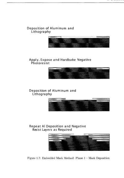
1.6.1 E m b ed d ed M ask M eth o d s for Large S cale T iered S tru ctu res
aluminum to deposit the masks for each elevation before any etching of the structure occurs. The variation in height between each elevation is a lim itation of the reactive ion etch (RIE) equipment in use. The Al-DMP process involves the following steps to create the masks:
1. Deposit 200 nm of Al and pattern
2. Pre-bake a t 200°C and deposit negative photoresist 3. Develop and hardbake
4. Deposit 200 nm of Al and p attern
Steps 2-4 of the deposition process are repeated as necessary to build the to tal number of masks required for the process. This process is shown graphically in Figure 1.7.
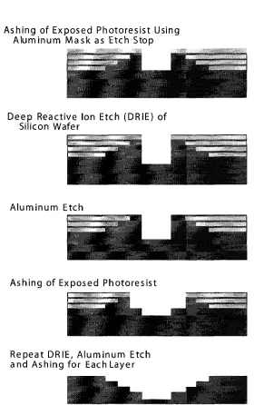
Once all the masks required are in place, a second processing phase transfers the p attern to the wafer. The etch process takes the following steps:
1. Ashing of exposed resist using Al mask 2. Deep ICP-RIE etch of exposed wafer 3. Al etch to remove mask layer 4. Ashing of exposed resist
Steps 2-4 of the etch process are repeated as necessary to etch all layers. This process is shown graphically in Figure 1.8. This process can be enhanced by placing a single layer of Si02 under the bottom Al layer. This Si02 layer provides protection for the structure against damage from Al pinholes when etching deep structures.
D e position o f A lu m in u m and
L ith o g ra p h y
zSBSEmmM
A p p ly, Expose and Hardbake Negative
Photoresist
De position o f A lu m in u m and
L ith o g ra p h y
Repeat Al Deposition and Negative
Resist Layers as Required
Ashing o f Exposed Ph otoresist Using
A lum inu m M ask as Etch Stop
Deep Reactive Ion Etch (DRIE) of
Silicon Wafer
A lu m in u m Etch
Ashing o f Exposed Ph otoresist
Repeat DRIE, A lu m in u m Etch
and Ashing fo r Each Layer
1.6.2
H and A ssem b ly for Low V olu m e, Low C o m p le x ity S tru ctu res
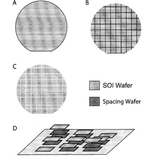
Hand assembly of the array from individual sensing surfaces provides a m ethod for m anufacturing low volumes of relatively simple arrays. In this m ethod, all sensors are m anufactured on a standard SOI wafer (Figure 1.9.A). By using an appropriate SOI wafer, the fabrication requires only a single mask. Optical lithography is used to transfer the etch mask to the wafer. A Bosch DRIE etch is performed to selectively expose the sacrificial Si02- The wafer is then submerged in BOE to release the diaphragms (Figure 1.9.B). After diaphragm release, the wafer is diced into individual sensing surfaces (Figure 1.9.C). These sensing surfaces are assembled manually by using techniques well- established in system-in-package fabrication (Figure 1.9.D). ‘Dummy’ wafers can be used to provide fixed height offsets and therefore very accurately control the out-of-plane tolerances. Mechanical tolerances in the out-of-plane axis can be controlled within 5/nn. Conductive epoxies are used to ensure ground plane connectivity during assembly. By using conductive epoxies, fabrication is vastly simplified as there is no longer a need to create metalized ground pads on the top of the wafer while avoiding the necessity of to wirebond to the bottom of the wafer.
B
\
/
C
pH
SOI Wafer
U
sPacin9 Wafer
D
1.7
P h ysical A p p lication R equirem ents
In 2005 the NHTSA m andated the use of advanced airbags in all new m otor vehicles sold in the USA. Critical to an advanced airbag system, are sensors and processing electronics to allow for autom atic and tailored airbag deployment based on seat occupancy. These systems must be able to determine the contents of a seat between Adult passengers, cargo, child safety seats and em pty seats. This information would allow the airbag to be autom atically disabled if the seat was empty, occupied by a rear facing child safety seat or the passenger was seated too close to the airbag for safe deployment. The criteria for designing these systems also apply to an external collision avoidance system:
• The selected frequency and pressure should not affect humans or animals likely to be in prox imity to a vehicle equipped w ith the system.
• N atural and artificial sound sources encountered while driving should not interfere w ith system operation.
• Vehicle crash sounds should not interfere w ith sensor operation.
• Ultrasound frequencies should be chosen to minimize signal attenuation in the media and maximize reflection from the target to allow a large signal to noise ratio (SNR) enabling accurate classification.
Hearing range d ata for many species was evaluated as well as human exposure limits. Cats and mice have some of the highest known hearing frequencies at 91 kHz and 100 kHz respectively. Con sequently frequencies over 100 kHz are desirable for these applications. Ultrasonic energy guidelines are defined separately for air-coupled and contact ultrasound. For air-coupled ultrasound, the two most plausible mechanisms for non-auditory effects are heating and cavitation. It has been reported th a t cavitation requires sound pressure levels (SPL) above 190 dB. Harmful effects will occur in humans for sound levels above 155 dB SPL. Current C anadian guidelines for continuous exposure to ultrasonic energy are listed in Table 1.2. The Canadian guidelines specify th a t for occupational exposure, the level must never exceed 137 dB under any circumstances [33].
Ta b l e 1 .2 : Ma x i m u m Ul t r a s o u n d Ex p o s u r e Le v e l s b y Fr e q u e n c y Frequency (kHz) SPL (dB)
16 75
20 75
25 110
31.5 110
40 110
50 110
frequencies, the peak acoustic pressure can exceed 110 dB SPL, adding support for the use of a frequency above 100 kHz for this sensor [34].
An additional requirement for the proof of concept design is manufacturability. The design must be easily fabricated using well established manufacturing techniques. In order to ensure the design can be fabricated economically and within tim e allowances, the proof of concept design will be subject to strict fabrication constraints. Performance of the sensor will be optimized w ithin these constraints.
1.8
Specific R esearch O bjectives
1. The development and exploration of the theoretical model for a non-planar MEMS based ultrasonic sensor microarray through the expansion of the theory developed by [19]. This includes investigating the key param eters and performance of the newly expanded model. 2. Using investigation d ata from the new model, create a generalized array design flow to allow
rapid development of arrays based on this topology. As far as it practical, this design flow will not be based on any specific fabrication technology.
3. Design a MEMS based ultrasonic sensor inicroarray for use as an enabling component of IAVSS system. The design will use the generalized array design flow to generate the geometry. A fabrication technology will be chosen and a detailed design of the sensing elements and array will be carried out.
5. Concurrent development of a fabrication process and m aterial selection w ith the sensor ana lytical design. The developed fabrication process is to use only standard MEMS fabrication techniques and materials to ensure manufacturability. The verified design process will be sim ulated to verify correct geometry and to guard against fabrication process incompatibilities.
1.9
P rin ciple R esu lts
The principle results of the research work presented in this thesis are summarized as follows: 1. A closed form generalized model for the array factor of a MEMS-based discretized hyperbolic
paraboloid geometry ultrasonic sensor m icroarray has been developed by extending the theory of macroscale continuous aperture hyperbolic paraboloid geometry transducer as presented in [19]. The new model has been verified against the original model for beamforming capabil ity and frequency response w ith excellent agreement. Additionally the new model supports placement of all elements parallel to the x-y plane for compatibility w ith MEMS fabrication techniques
2. The developed sensor m icroarray can intrinsically provide a broadband, constant-beam width, beamforming capability w ithout any microelectronics based signal processing as necessary for conventional planar beamforming sensor arrays. This enable to sensor m icroarray to be used in real-time applications where split-second decisions are necessary, for example in autom otive collision avoidance systems.
3. A generalized array design methodology has been developed based on the newly developed model. This provides an easy method to determine the array physical design specifications, such as: array side length and height, number of elevations (tiers), number and spacing of sensing surfaces based on the desired array response, sensing scheme selection, design and behaviour simulation of sensors and verification.
5. MEMS-based capacitive type ultrasonic sensor have been chosen to constitute the array el ements (sensing surfaces). Extensive analytical and FEA analysis has been performed to characterize and verify the behaviour of MEMS based capacitive type acoustical sensors. The analytical and 3-D coupled domain FEA results are in close agreement th a t verifies the design. 6. A silicon-on-insulator (SOI) based-fabrication process table has been developed in consulta tion with the A lberta nanofab facility and simulated using IntelliSuite to fabricate the array geometry developed for the IAVSS application. Array assembly and packaging information was determined and verified in conjunction with the CMC Microsystems.
1.10
O rganization o f T h esis
C hapter 2 deals w ith introducing the fundamentals of array based beamforming. From this foun dation the extension into using shaped arrays to provide beamforming functionality is introduced. Existing work on hyperboloid paraboloid shaped arrays is presented. The existing theory is then expanded upon to include discrete arrays. A closed form model of the array factor for the discrete hyperbolic paraboloid shaped array is presented.
In C hapter 3 the beamforming theory developed previously is applied in the creation of a sys tem atic method for hyperboloid paraboloidal MEMS compatible array design. The step by step procedure is given, as well as a numerical example. Equations based on extensive simulation d ata are presented to provide guidelines during array design. The procedure contained in this chap ter is fabrication technology and transduction domain independent. The specific design procedure required for using the generated array geometry as a MEMS acoustic array are detailed next.
C hapter 4 introduces MEMS based acoustical sensors. The m ajor transduction m ethods are reviewed. A lumped element model is used to allow the rapid determ ination of the design param eters for MEMS based acoustic sensors. The lumped element results are then verified against finite element analysis. The results show excellent consistency between the two methods.
C hapter 5 details fabrication related m aterial. The array fabrication table is overviewed. Each m ajor fabrication step is shown including simulation results. This process cumulates in the completed array.
N o n -P la n a r B e a m fo rm in g
In contrast to planar sensor array geometries, a non-planar array refers to a one or two dimensional array where the sensor elements are distributed at different elevations along the vertical axis. The objective of constructing a non-planar array geometry is to obtain a better array response over the desired frequency range as compared to planar geometries. In this chapter the theory of a continuous aperture hyperbolic paraboloid geometry acoustical transducer is reviewed. Based 0 1 1
the review, a m athem atical model for the array response of a discretized hyperbolic paraboloid geometry non-planar array th a t can be fabricated using state-of-the-art microfabrication techniques has been developed.
2.1
T heory o f H yp erb olic P araboloid G eom etry A cou stical
Transducer
The overall beam p attern of an array of sensors depends on five key param eters as listed below [35]: 1. The geometric configuration of the array elements (shape of the array)
2. Inter-element spacing 3. Element sensitivity
5. The beam p attern of the individual elements
The array factor of a one-dimensional uniform array (array elements feature identical sensitivity, directional response and inter-element spacing) can be expressed as:
where N is the number of elements in the array, u> is the frequency in radians, c is the speed of sound in the medium, d is the inter-element spacing and 9 is the angle of incidence.
By decoupling the array behaviour from the sensing element behaviour, the array and the sensing elements can be designed independently. This separation reduces the complexity level of the design. It also facilitates the creation of a general, technology independent methodology for hyperbolic paraboloid shaped array design.
A hyperbolic paraboloid surface as shown in Figure 2.1 satisfies the requirements for providing an intrinsic broadband constant beamwidth beamforming operation in 2 dimensions. A hyper bolic paraboloid-shaped continuous aperture transducer uses the transport delay associated w ith the curved nature of the sensing surface to m aintain a constant beamwidth over a wide operating frequency range. No microelectronics-based signal processing is necessary for the beamforming op eration. The beamwidth depends on the out-of-the plane twist of the hyperbolic paraboloid-shaped surface and is independently specified in each axis by the out-of-plane angle measured in degrees from the center of the array present at the array extremities [19, 20].
In the C artesian coordinate system, a square footprint hyperbolic paraboloid surface can be expressed as [20]:
W here x, y and z are the Cartesian coordinates, L is th e sidelength in wavelengths in the x and
measured in degrees from the center of the surface as shown in Figure 2.1.
The far-field directional response, or array factor, of a continuous aperture hyperbolic paraboloid shaped acoustical sensor of side length L in a given direction (9, <j>) as referenced from the array normal is expressed as (2.3) [20]:
(2.1)
(2.2)
y directions and a is the am ount of out-of-plane twist in the z direction at the surface extrem ity
j27rt I x ta n 6 + y ta n </> +
dydx (2.3)
L _ Y
M ain lo b e - 3 dB C ross Sectio n S h a p e by F req u en cy
3 lam b d a
— 5 lam b d a
— * 8 lam b d a
■ • * * 15 lam b d a
<D a>
cn
a) Q Z
a .
-10
-1 0 •5 0 5 10 15
T h e ta D e g re e s
Figure 2.2: Beamforming w ith the Continuous Aperture Sensor
where Y is the array sidelength in the y direction, L is the array sidelength in x direction, and a is the out-of-the plane angle at the array extremities in b o th x and y directions, respectively. The param eter t in (2.3) is defined as:
ta n 2 6 + ta n 2 0 + 1
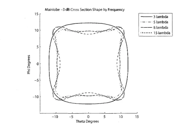
Equation (2.3) assumes th a t the out-of-plane angle a is small and the sensor sidelengths L and Y are expressed in units of wavelengths of the desired acoustic frequency. It has been shown th a t for a large L w ith a small out-of-plane angle a , the directional response of the sensor has a reasonably constant value of — [20]. It has also been determined th a t a < 10° results in a reasonably
2 aL
constant beamwidth of 2a whereas for a > 10° (2.3) cannot be used to determine the beam shape accurately due to m athem atical assumptions made during its derivation. Cross-sectional views of the mainbeam a t -3dB are presented in Figure 2.2. This clearly shows the efficacy of the intrinsic broadband beamforming in the continuous aperture sensor.
above this, the beamwidth remains stable.
The intrinsic beamforming capability of this geometry is highly desirable for use in a m icroarray to minimize system power consumption and cost, while taking advantage of the scaling benefits offered by microfabrication. Due to the curved nature of the Hyperbolic Paraboloid surface, it is incompatible w ith the current state-of-the-art microfabrication techniques as they are based on planar operations.
Following synthesis theory commonly used in antenna design, it is possible to emulate the be haviour of a large continuous aperture sensor through the use of an array of smaller sensors [35]. The double integral expressing the array response in (2.3) can be expressed as the sum of an infinite number of discrete points separated by infinitesimal intervals using the spatial sampling technique. Each discretized value would represent a level or sensing surface in a 3-D space. This array of sensors located at different elevations (non-planar), resembling a discretized hyperbolic paraboloid surface, could be realized using the conventional planar microfabrication techniques.
The fundam ental theorem of Calculus states th a t the double integral in (2.3) can be discretized by using the Riemann summation [36]. After performing spatial sampling using the Riemann sum mation, the infinite summation can be reduced to a finite one of an arb itrary number of levels. Due to the loss of sensing elements after reduction, it is expected th a t there may be some performance degradation of the array response. A conceptual geometry of a discretized hyperbolic paraboloid surface is shown in Figure 2.3. However, care m ust be taken to ensure th a t the geometric approxima tion remains suitably accurate to allow operation over the desired frequency range. This lim itation is explored in depth in C hapter 3. Counter to the desire for an accurate representation of the ge ometry are the demands of manufacturability. Too many elevation levels may make the fabrication process complex, as each of the elevations may hold one or more sensing surfaces. The process used to generate the discrete geometry is shown graphically in Figure 2.4.
From the different variations of the Riemann summation, derivations based on the center-based Riemann summation are used due to their accuracy for non-monotonic functions, and the ability to calculate error bounds [36]. The center-based Riemann summation in one dimension can be expressed as [36]:
Jf ^dx = ^ t ‘f {a+(i+l ) ^ r ) ^ r
( 2 - 5 )a i—1
Figure 2.3: Seven Elevation Discrete Hyperbolic Paraboloid
Finite Sum m ation Hyperbolic Paraboloid C o n tin u o u s H yperbolic
P arab o lo id
Infinite Sum m ation Hyperbolic Paraboloid
o
J
f { x ) d xwhere M2 is the maximum value of \ f (a;)| and A mici is the value of f ( x) at the m idpoint of the interval a-b.
Applying (2.5) to (2.3) along the x axis yields:
M -1 |
f
( ^ ) t a n d +y t & n i p
+ " " ' I
''l .
=
J
'
V
' t *
(2-7)
m = 0 y
— T
The transform ation is then applied a second time along the y axis to obtain the discretized array response as:
( ’ 1 , 1 2alx )(y )
m-i j v- i j 2 7 r t I (a; ) t a n 0 + ( y ) t a n 0 H
---f(d, <f>)
= ----
lim limV"' V '
eV
) (2.8)v M N M —>oo N —>oc ^ ^ y ’
m= 0 n= 0
where:
Equation (2.8) is the array response from a discretized hyperbolic paraboloid surface where the param eters M and N represent the number of sensing surfaces in the x and y directions respectively. Finally, (2.8) can be reduced to a finite summation as expressed in (2.10) where M and N are finite integers.
M - X N - i j 2 n t ((x ) ta n 0 + (y )tan</>+ ^ ^
' m - s E E - v l
'
< 2 - 1 0 >m— 0 n = 0
Equation (2.10) represents the array factor for a discretized hyperbolic paraboloid geometry sensor array. The minimum sidelength S (in meters) of a square footprint hyperbolic paraboloid geometry array can be determined using the following relation:
S m i n = ( 2 . 1 1 )
J lo w e r
where c is the speed of sound in the media and f i OWe r is the lower bound of the operating
5 L am bda F re q u en c y M ain lo b e S h a p e C o m p ariso n
3x3 T ran sd u cers
5x5 T ran sd u cers
9x9 T ran sd u cers
C o n tin u o u s A p e ra tu re
oj <u Oi <u o c - 5 .c CL
- 1 0
- 1 5
- 2 0
10 20
- 1 0 0
- 2 0
T h e ta (in D egrees)
Figure 2.5: Main Beam -3dB Cross-Sections of Continuous and Discrete Arrays
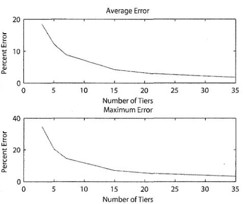
Values for K can range between 3 and 10 (see section 3.1). The array response as expressed in (2.10) has been verified by comparing results from the integral model as expressed in (2.3). The results converge exceedingly well even for low values of M and N. The results converge even for M = N = 3 when the array sidelengths correspond to 5A where A is the wavelength of the lower bound of the operating frequency. The difference between the array responses from (2.3) and (2.10) for a 3 sensing surface per axis implementation averages less then 18% in the passband. Although this seems like a large error, investigation shows th a t the prim ary source of this error is a small shift of the main beam. This can be seen in the -3dB cut-off as shown in Figure 2.5. W ithin the passband region, the responses remain significantly identical. This error can be reduced significantly as shown in Figure 2.6, by increasing the number of tiers. From Figure 2.6, it appears th a t the average beamshape error can be reduced to < 5% w ith only a m oderate number of tiers.
The 3-D beam p attern of a discretized square footprint hyperbolic paraboloid surface is shown in Figure 2.7 for a sidelength of 5A and 15A where A is the wavelength of the operating frequency lower bound. Figure 2.7 clearly establishes th a t it is possible to construct a frequency-independent broadband beamforming sensor m icroarray w ith discrete array elements by exploiting the surface topology.
A verage Error
20
10
0
25 30 35
0 5 10 15 20
N u m b er o f Tiers M axim um Error 40
20
0
25 30 35
0 5 10 15 20
N u m b er o f Tiers
Figure 2.6: Worst Case Passband Approximation Error
A rray Factor: 5 L am b d a S id e le n g th Array Factor: 15 L a m b d a S id e le n g th
Phi C T \ /
In d e g r e e s 2 d ^ - 2 0 Phi o \ In d e g r e e s T h e ta
In d e g r e e s \ / T h e ta
20 -20 In d e g r e e s
Mainlobe -3db Cross Section Shape by Frequency
---3 la m b d a --- 15 lam b d a 15 • — 5 la m b d a 15r 21 lam b d a
-10 -5 0 5 10 15 -10 -5 0 5 10 15
Theta Degrees Theta Degrees
Figure 2.8: Cross-Sectional Changes in Beamshape Over Change in Lam bda
A r r a y D e sig n
In this chapter, the design methodology for an acoustic sensor array based on the discretized hy perbolic paraboloid geometry is presented. The methodology is based 0 1 1 the m athem atical model
developed in the previous chapter. The presented generalized methodology is fabrication technology independent and can be tailored to accommodate specific design requirements and the fabrication processes available in a standard foundry within certain limitations. Once the desired operating frequency range, beamwidth and acceptable beamwidth variation within the operating frequency range are specified, the methodology enables the determ ination of the geometric specifications for the array. This occurs in a straightforward mariner by following a set of m athem atical relations developed from an exploration of the m athem atical model from C hapter 2.
3.1
D eterm in ation o f A rray Sidelen gth
The array sidelength can be determined from:
Kc
S „ n n = --- (3.1) J lo w e r
T a b l e 3 .1 : B e a m w i d t h C o n t r o l P a r a m e t e r K V a l u e s
K (unitless) Beamwidth Variation)0)
3 7
5 5
8 2
10 1
■e
range of 1 — 10° variations for all the frequencies in a frequency range of = 40. This range of frequency appears to be sufficient for most applications. For example, for a value of K = 10, the maximum beamwidth variation for all the frequencies in the range is less th an 1° whereas for K = 3, the maximum variation increases to 7°. Following (3.1), for a fixed f i o w e r , lowering K reduces the array sidelength a t the expense of a wider beamwidth variation. Table 3.1 lists the determ ined beamwidth variations expected for different K values for a frequency range where Jppper' < 40.
3.2
D eterm in in g th e N um ber o f Sensing Surfaces
Following (2.10), the constant beamwidth property over the operating frequency range of the dis cretized hyperbolic paraboloid geometry array is a direct function of the number of the sensing surfaces. Typically, the Nyquist criteria for spatial sampling provides a m ethod to determ ine the inter-element spacing, and by extension, the number of sensing surfaces present in the array. This criteria specifies th a t the main lobe power is maximized for the frequency where the inter-element spacing is equal to A/2 where lam bda is the wavelength of the operating frequency. However, for a frequency range, satisfying the Nyquist criteria isn’t possible for all frequencies. Thus, applying the Nyquist criteria to determine the spacing between the sensing surfaces in the discretized hyperbolic paraboloid geometry array will predict an erroneous result, even if the wavelength associated w ith the center frequency in the desired frequency band is used to determine the spacing between the sensing surfaces.