ISSN (Print) : 2347 - 6710
International Journal of Innovative Research in Science, Engineering and Technology
Volume 3, Special Issue 3, March 2014
2014
I
nternational
C
onference on
I
nnovations in
E
ngineering and
T
echnology (ICIET’14)
On 21st&22nd March Organized byK.L.N. College of Engineering, Madurai, Tamil Nadu, India
ABSTRACT— There are two proposed converters in this paper, one of which is inverting while the other is non-inverting.. Both converters work on the principle of resonance and the active elements operate under soft-switching conditions. The topology is similar to that of SEPIC converter, but the operation is different. In fact, inductors and Capacitor create coupling networks. The circuit has been simulated using MATLAB Simu-link. Simulation results are verified.
KEYWORDS— Resonant converter, soft-switching,
step-down/upconverter, zero current switching (ZCS)
I. INTRODUCTION
Soft-switching techniques are developed to reduce switching losses and electromagnetic interference (EMI). At soft-switching condition, switching frequency can be increased to enhance the converter power density. This conditionis commonly attained by zero voltage switching (ZVS) and zero current switching (ZCS)[1]. An insulated gate bipolar transistor (IGBT) is a proper switch for power applications. ZCS technique is compatible with the buck-boost type converters include the basic pulse width modulation (PWM) buck-boost and Cuk converters, which provide negative voltage gain, and, single ended primary inductor converter (SEPIC) and Zeta converters which provide positive voltage gain. These converters are widely employed as power supplies and PFC regulators. In Cuk, SEPIC, and Zeta converters, the coupling capacitor is the main energy storage element and thus its voltage should be almost constant. A significant disadvantage is the requirement of a large capacitor with a high ripple-current carrying capability[1]. Various methods have been presented in the literature to provide soft-switching condition for the SEPIC converter[2][3]. Almost all of these methods preserve the overall operation
switching condition by adding auxiliary elements. The number of added elements is between 2 for quasi-resonant type in complex cells[4][5]. However, the number of elements of a converter is one of the most important considerations, since it greatly affects on the converter cost and volume[6].
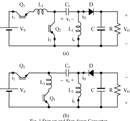
Fig. 1.Step up and Step down Converter
In this paper, two new resonant step-down/up dc–dc converters are presented where both haveexactly the same operation except the sign of voltage gain Fig. 1(a) and (b). All switches are turned on and off at ZCS and the diode operates at ZCS or ZVS. In view of step down/up voltage gain with positive output voltage polarity and the general topology of the proposed circuit as shown in Fig. 1(a), it is very similar to the SEPIC converter with only one extra switch at input. The coupling capacitor Cr which still provides magnetic isolation, is now a resonant capacitor and hence its capacity becomes much less than that of the conventional
Design and Implementation of New
Resonant Step Down/Up Converters
S.Rathnaprabha
#1, K.R.Vairamani
*2#1
Department of Instrumentation & Control Engineering, Saranathan college of engineering, Tiruchirapalli, India
Copyright to IJIRSET www.ijirset.com 2
M.R. Thansekhar and N. Balaji (Eds.): ICIET’14
SEPIC converter. Consequently, the operation of the proposed converters is completely different than the conventional SEPIC converter. In other words, in the proposed converters, Cr and inductors constitute resonance networks. The transistors Q1 and Q2 , which in fact construct a half-bridge structure, are unidirectional switches and thus energy does not return to source. Moreover, the inductor L1 eliminates the spiky current flowing through the on switch and the output capacitance of the off switch. The converters can operate at DCM and CCM where soft-switching condition is always attained independent of load and operating voltages. In the proposed topologies, soft-switching condition is provided by adding only one extra element, and current stresses and size of the passive components are considerably reduced. All these merits are obtained only at the cost of relatively higher voltage stress of one of the switches. However, in comparison to current stress and energy circulation, voltage stress does not produce extra conduction losses. Thus, the proposed converters are suitable for high current applications but not suitable for high voltage purposes. In comparison with the conventional SEPIC converter, the input current is discontinuous. Considering the major advantages created by this topology, an LC filter can be added at the input to make the source current continuous if deemed necessary.
II. ANALYSIS OF CONVERTER
Both proposed converters have four operating conditions; two states at discontinuous conduction mode (DCM) and two states at continuous conduction mode (CCM). These conditions are viewed for the current of L2which is
defined as resonance current, ir.In the following
discussions, the converter of Fig. 1(a) is considered. To simplify the analysis, it is assumed that the converter is in steady state, all elements are ideal, and output capacitor C
is large enough such that the output voltage is constant during one switching cycle. Following definitions are made:
L= L1 + L2 (1) α=L2/Lr, α≤ 1 (2) ωr=1/√(LrCr)
fr=1/Tr=ωr/2π(3)
Zr=√Lr/Cr (4) r=𝑅/𝑍r (5)
A =|VO| / VS .(6)
In the converter of Fig. 1(a), assume that the resonance voltage isVr =VO , and all semiconductor devices are off.
By turning Q1 on at t = t1 , the voltage across L2 is as (7).
Thus D does not turn on if V L2 (t+ 1 )< VO, or α < A/(1 +
A)
V L2 (t1+ ) = (L2/L1 + L2 ) x (VS + VO)(7)
For the DCM Operation with α < A/(1 + A) the corresponding modal analysis is as follows.
A.Mode I (t1 − t2):
At t1 , Q1 is turned on at ZCS and Cr is charged through a
resonance with L1 and L2. At t2, ir reaches zero and Q1 is
turned off at ZCS. At this time Vr has reached 2VS + VO
Fig. 2. Mode I (t1-t2)
Vr(t) /VS= 1− (1 + A) cos(ωr(t − t1 )) (8)
ir(t) = (VS+ VO/Zr )sin(ωr(t − t1 )) (9)
t2−t1=Tr/2.(10)
B.Mode II (t2− t3):
At t2, Q2is turned on at ZCS and the polarity of Vrstarts
reversing until it reaches −VO at t3
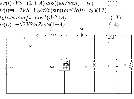
Vr(t) /VS= (2 + A) cos((ωr/√α)t1 − t2 ) (11)
ir(t)=(−2VS+VO/αZr)sin((ωr/√α)t1−t2 )(12)
t3-t2=√α/ωr[π–cos-1(A/2+A) (13) ir(t3)=−√2VS/αZrx√(1+A) (14)
Fig 3. Mode II (t2-t3) C.Mode III (t3− t4):
At t3 , the diode D becomes forward biased at ZVS, hence
Vr stays constant at−VO and iris diverted to the diode
since C is much larger than Cr . The magnitude of
irdecreases linearly until at t4it reaches zero. At this time
D is turned off at ZCS. Any time during this mode Q2can
be turned off at ZVZCS. The entire energy absorbed by Cr in Mode I is now pumped to the output
ir(t)=ir(t3)+VO/L2x(t2−t3) (15)
t4−t3=(2√α/ωr)(√(1+A)/A) (16) D.Mode IV (t4 − t5):
In this mode, all switches are off and the load is supplied by the output capacitor. Duration of this interval is determined by the controller, so that proper voltage regulation is attained (dead time control). According to the equivalent circuits of each operating mode, all stray inductors and the switches parasitic inductances are absorbed by L1and L2. Since the diode is turned on at
other words, when Q2is turned on, C and Cr are set in
parallel with D.
Fig 4. Mode IV (t4-t5)
These features are common characteristics in the all-remaining states as discussed in the following paragraphs. At steady state, the converter voltage gain A can be calculated by satisfying energy conservation principle in one switching cycle as (17) where fS= T S −1is
the switching frequency. By substituting (9) in (17), and defining S as (18), A is obtained as (19)
∫TSVSi1dt=∫TSvo2/Rdt (17) S=2RCrfS=(r/π)(fS/fr)(18)
S =(A2/1 + A)
A=(S+√(S2+4S))/2 (19)
In the absence of dead time (Mode IV), the converter operates at its maximum power handling capability where the switching frequency is also at maximum. By substituting TS = t4− t1in (18) and applying (10), (13), and
(16), maximum attainable voltage gain Amis obtained.
This equation is required for the converter design
III.SIMULATION
A. Buck Mode Converter:
The Simulation circuit for buck mode converter is shown in Fig 5.The input DC waveform is given as 15V which is shown in the Fig 6.
Fig. 5. Simulation circuit for Buck Mode Converter
The Gate Source voltage and Drain source voltage across switch 1 of the Buck mode converter is shown in Fig 7and Fig 8 respectively.
Time(ms)
0.0113 0.0113 0.0113 0.0113 0.0113 0.0113 Time(ms)
Fig.7.Gate Voltage across Switch 1
Time(ms)
Fig.8.Drain Source Voltage across switch1
Similarly, the Gate voltage and Drain Source voltage of Buck mode converter across switch 2 is shown in Fig.9 and Fig.10 respectively.
0.0168 0.0168 0.0168 0.0168 0.0168 0.0168 0.0168 0.0168
Time(ms)
Fig.9Gate Voltage across switch 2
ag
e
(V
)
V
o
lt
ag
e
V
d
s (V
)
V
o
lt
ag
e
V
g
(V
)
V
o
lt
ag
e
V
d
s(
V
)
C
ap
ac
it
o
r
v
o
lt
ag
e
(V
)
G
at
e
V
o
lt
ag
e
V
g
(V
Copyright to IJIRSET www.ijirset.com 4
M.R. Thansekhar and N. Balaji (Eds.): ICIET’14
Time(ms)
Fig 10.Drain Source Voltage across Switch 2
The voltage and Current flowing through the Capacitor Cr
, are shown in Fig 11 and Fig.12 respectively.
0.0169 0.0169 . 0.0169 0.0169 0.0169 0.0169 0.017 0.017
Time(ms)
Fig 11.Voltage across Capacitor Cr
Time (ms)
Fig 12.Current acrossCapactior Cr
The current flowing through the Diode in series with resonant capacitor Cr is shown in Fig.13
.
Time(ms)
Fig 13.Current across diode
The output voltage of the Buck mode converter is shown in the Fig.14.The output voltage is usually obtained in the range of 5V-6V for the given input voltage 15V. Thus the input output relation is nearly Vo= 3Vs
Time(ms)
Fig.14. DC output Voltage
B.Boost mode converter:
The Simulation circuit for buck mode converter is shown in Fig 15.The input DC waveform is given as 30V which is shown in the Fig 16.
Fig 15. Simulation Circuit for Boost mode converter
Time(ms)
Fig 16. DC input Voltage
The Gate Source voltage and Drain source voltage across switch 2 of the Buck mode converter is shown in Fig 17 and Fig 18 respectively.
0.2196 0.2196 0.2196 0.2196 0.2196 0.2196 0.2196 .
Time(ms)
Fig.17. Gate Voltage across Switch 2
Time(ms)
Fig.18. Drain Source Voltage across Switch 2
The voltage and Current flowing through the Capacitor Cr , are shown in Fig 19 and Fig.20 respectively.
C
ap
ac
it
o
r
C
u
rr
en
t(
A
)
D
io
d
e
C
u
rr
en
t(
A
)
V
o
lt
ag
e(
V
)
V
o
lt
ag
e
(V
)
V
o
lt
ag
e
V
g
(
V
)
V
o
lt
ag
e
V
d
s (V
5.01 5.02 5.03 5.04 5.05 5.065.07 5.08 5.09
Time(ms)
Fig.19. Voltage across Capacitor Cr
Time(ms)
Fig.20. Current across Capacitor Cr
The current flowing through the Diode which is connected in series with the resonant capacitor Cr is shown in Fig.21
Time(ms)
Fig.21. Current across Diode
The output voltage of the Buck mode converter is shown in the Fig.14.The output voltage is usually obtained in the range of 29V-30V for the given input voltage 15V. Thus the input output relation is nearly Vs= 2Vo
Time (ms)
Fig.22. DC output Voltage
IV.DESIGN VALUES:
These values are calculated based on the formulae mention above for both stepup/stepdown conduction: 1. Vo=6v,vin=15, αmin=0.30
2. r=0.68,R=75 3. Zr=119 ohm 4 .ωr= 78kHZ
5. L2=350µH,.L1=42µH,L=392µH 6 .C1=49.5nF, C2=500µH
V.CONCLUSION
Two new resonant step-down/up converters were presented where all active elements operate under soft-switching condition independent of load and operating voltages. In the proposed converters, inductors and coupling capacitor create resonant networks. Thereby, not only soft-switching condition is achieved,but also the passive components size is small. The converters can operate in DCM and CCM.
REFERENCES
[1] N. Mohan, T. M. Undeland, and W. P. Robbins, Power Electronics: Converters, Applications, and Design, 3rd ed. New York: Wiley, 2002. [2] C.-L. Shen, Y.-E.Wu, and M.-H. Chen, “A modified SEPIC converter with soft-switching feature for power factor correction,” in
Proc. IEEEInt. Conf. Ind. Technol., 2008. ICIT 2008, Apr., pp. 1–8. [3] E. Adib and H. Farzanehfard, “Family of soft-switching PWM converters with current sharing in switches,” IEEE Trans. Power.Electron., vol. 24, no. 4, pp. 979–985, Apr. 2009.
[4] C.-M. Wang, “A new family of zero-current-switching (ZCS) PWM converters,”IEEE Trans. Ind. Electron., vol. 52, no. 4, pp. 1117–1125, Aug. 2005.
[5] H.-S. Choi and B. H. Cho, “Novel zero-current-switching (ZCS) PWM switch cell minimizing additional conduction loss,” IEEE Trans. Ind.Electron., vol. 49, no. 1, pp. 165–172, Feb. 2002.
[6]MasoudJabbari and HoseinFarzanehfard, “New Resonant Step down/Up converters”,”IEEE Trans Power Electronics, vol25,no.1,Jan 2010
C
ap
ac
it
o
r
V
o
lt
ag
e
(V
)
C
ap
ac
it
o
r
C
u
rr
en
t
(
A
)
D
io
d
e
C
u
rr
en
t
(
A
)
V
o
lt
ag
e(
V