University of Windsor University of Windsor
Scholarship at UWindsor
Scholarship at UWindsor
Electronic Theses and Dissertations Theses, Dissertations, and Major Papers
1-1-2019
Hardware Implementation of Bit-Parallel Finite Field Multipliers
Hardware Implementation of Bit-Parallel Finite Field Multipliers
Based on Overlap-free Algorithm on FPGA
Based on Overlap-free Algorithm on FPGA
Meitong Pan
University of Windsor
Follow this and additional works at: https://scholar.uwindsor.ca/etd
Recommended Citation Recommended Citation
Pan, Meitong, "Hardware Implementation of Bit-Parallel Finite Field Multipliers Based on Overlap-free Algorithm on FPGA" (2019). Electronic Theses and Dissertations. 8175.
https://scholar.uwindsor.ca/etd/8175
This online database contains the full-text of PhD dissertations and Masters’ theses of University of Windsor students from 1954 forward. These documents are made available for personal study and research purposes only, in accordance with the Canadian Copyright Act and the Creative Commons license—CC BY-NC-ND (Attribution, Non-Commercial, No Derivative Works). Under this license, works must always be attributed to the copyright holder (original author), cannot be used for any commercial purposes, and may not be altered. Any other use would require the permission of the copyright holder. Students may inquire about withdrawing their dissertation and/or thesis from this database. For additional inquiries, please contact the repository administrator via email
Bit-Parallel Finite Field
Multipliers Based on Overlap-free
Algorithm on FPGA
By
Meitong Pan
A Thesis
Submitted to the Faculty of Graduate Studies
through the Department of Electrical and Computer Engineering
in Partial Fulfilment of the Requirements for
the Degree of Master of Applied Science
at the University of Windsor
Windsor, Ontario, Canada
2019
c
Hardware Implementation of Bit-Parallel
Finite Field Multipliers Based on Overlap-free
Algorithm on FPGA
By
Meitong Pan
APPROVED BY:
S. Cheng
Department of Civil & Environmental Engineering
B. Balasingam
Department of Electrical & Computer Engineering
H. Wu, Co-Advisor
Department of Electrical & Computer Engineering
M. Mirhassani, Advisor
Department of Electrical & Computer Engineering
I hereby certify that I am the sole author of this thesis and that no part of this
thesis has been published or submitted for publication.
I certify that, to the best of my knowledge, my thesis does not infringe upon
anyone’s copyright nor violate any proprietary rights and that any ideas,
tech-niques, quotations, or any other material from the work of other people included
in my thesis, published or otherwise, are fully acknowledged in accordance with
the standard referencing practices. Furthermore, to the extent that I have
in-cluded copyrighted material that surpasses the bounds of fair dealing within the
meaning of the Canada Copyright Act, I certify that I have obtained a written
permission from the copyright owner(s) to include such material(s) in my thesis
and have included copies of such copyright clearances to my appendix.
I declare that this is a true copy of my thesis, including any final revisions, as
approved by my thesis committee and the Graduate Studies office, and that this
thesis has not been submitted for a higher degree to any other University or
Institution.
Abstract
Cryptography can be divided into two fundamentally different classes:
symmetric-key and public-symmetric-key. Compared with symmetric-symmetric-key cryptography, where the
com-plexity of the security system relies on a single key between receiver and sender,
public-key cryptographic system using two separate but mathematically related
keys. Finite field multiplication is a key operation used in all cryptographic
sys-tems relied on finite field arithmetic as it not only is computationally complex but
also one of the most frequently used finite field operations.
Karatsuba algorithm and its generalization are most often used to construct
mul-tiplication architectures with significantly improved in these decades. However,
one of its optimized architecture called Overlap-free Karatsuba algorithm has been
mention by fewer people and even its implementation on FPGA has not been
men-tioned by anyone. After completion of a detailed study of this specific algorithm,
this thesis has proposed implementation of modified Overlap-free Karatsuba
algo-rithm on Xilinx Spartan-605. Applied this algoalgo-rithm and its specific architecture,
reduced gates or shorten critical path will be achieved for the given value of n.
Optimized multiplication architecture, generated from proposed modified
Overlap-free Karatsuba algorithm and applied on FPGA board,over NIST recommended
fields (n = 128), are presented and analysed in detail. Compared with existing
works with sub-quadratic space and time complexities, the proposed modified
al-gorithm is highly recommended module and have improved on both space and
time complexities. At last, generalization of proposed modified algorithm is
suit-able for much larger size of finite fields, and improvements of FPGA itself have
been discussed.
my grandparents
my parents
my fianc´
e
for their unconditional love
and
support
Acknowledgments
I wish to express my sincere gratitude to my supervisor Dr.Mitra Mirhassani and
my co-supervisor Dr. Huapeng Wu, for their patience, motivation and immense
knowledge throughout my graduate study.
I would like to thank my family members, my mum, dad and my fianc´e, for their
constant support and continuous encouragement during the time of completing
my further study.
I would like to thank my committee members, Dr. Huapeng Wu, Dr. Bala
Bal-asingam and Dr. Shaohong Cheng.
I would also like to thank my colleagues at Uwindsor’s Faculty of Electrical and
Computer Engineering, especially Andria Ballo,for their help and support.
Declaration of Originality iii
Abstract iv
Dedication v
Acknowledgments vi
List of Figures ix
List of Abbreviations x
1 Introduction 1
1.1 Motivation . . . 1
1.2 Objective . . . 3
1.3 Organization of Thesis . . . 5
2 Preliminary 6 2.1 Mathematics Fundamental . . . 6
2.2 Finite Field . . . 8
2.3 Arithmetic Operation in Finite Field GF(2n) . . . . 9
2.3.1 Arithmetic operation in complex number field . . . 10
2.3.2 Arithmetic operation in Finite FieldGF(2n) . . . 10
2.4 Multiplication Architectures . . . 11
2.4.1 Bit-parallel multiplication . . . 12
2.4.2 Bit-serial multiplication . . . 12
3 An Overview of Bit-Parallel Multiplication for GF(2n) and Com-parison 14 3.1 Karatsuba Algorithm . . . 14
Table of Content viii
3.2 Overlap-free Karatsuba-Ofman Algorithm . . . 16
3.3 Reconstructed Karatsuba Algorithm . . . 19
3.4 Improved Reconstruction by Bernstein . . . 21
3.5 Comparison . . . 21
4 Proposed Hardware Implementation of Modified Overlap-free Karatsuba Multiplication Algorithm for GF(2n) 26 4.1 Fundamental Technology Background . . . 27
4.1.1 FPGA and their internal architecture . . . 27
4.1.2 Verilog HDL and ISE Design Suite . . . 29
4.2 Hardware implementation of Modified Overlap-free Karatsuba al-gorithm for GF(2n) on FPGA . . . 31
4.2.1 Fundamental Multiplication Modules for GF(24) . . . 32
4.2.2 Implementation of proposed modified algorithm for GF(2n) on FPGA . . . 35
4.3 Complexity Comparison . . . 39
4.3.1 Synthesis results . . . 39
4.3.2 Comparison . . . 40
5 Conclusion 44 5.1 Summary of Contribution . . . 44
5.2 Future Work . . . 45
Bibliography 47
Appendix A 51
Appendix B 54
3.1 Ranges of x’s exponents of equation (3.1) . . . 17
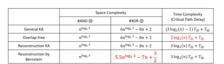
3.2 Comparison time and space complexities of four different multipli-cation algorithms . . . 22
3.3 Horizon direction comparison . . . 23
3.4 Comparison in the number of XOR gates . . . 23
3.5 Comparison in time complexity . . . 24
4.1 Internal architecture of a typical FPGA . . . 27
4.2 Basic simulation arrangement . . . 30
4.3 Project Navigator Interface [24] . . . 31
4.4 Multiplier Architecture by applying Overlap-free KA . . . 34
4.5 RTL Schematic . . . 37
4.6 2, 4, 5 and 6-input LUTs . . . 38
4.7 ISim simulation without input module . . . 38
4.8 ISm simulation with proposed input module . . . 39
4.9 Simulation result of proposed modified module for GF(24) . . . 40
4.10 Simulation result of proposed modified module for GF(28) . . . 40
4.11 Simulation result of proposed modified module for GF(216) . . . 40
4.12 Comparison of device utilization and combinational path delay of proposed modified multipliers and other multipliers for GF(24) . . . 41
List of Abbreviations
DES Data Encryption Standard
AES Advanced Encryption Standard
ECC Elliptic Curve Cryptography
KOA Karatsuba-Ofman’s algorithm
VLSI Very-Large-Scale Integration
CPF Component Polynomial Formation
NIST National Institute of Standards and Technology
FPGA Field-Programmable Gate Array
CLB Configurable Logic Blocks
LUT Look-up Table
FF Flip-Flop
MUX Mutiplexer
IOB Input / Output Blocks
HDL Hardware Description Language
RTL Register Transfer Level
ISE Integrated Synthesis Environment
KA Karatsuba Algorithm
ETP Even-Term Polynomial
RKA Recursive Karatsuba Algorithm
MKM Modified Karatsuba Multiplier
Introduction
With the rapid development of computer network technology, the application of
the Internet has become more extensive. The openness of the Internet brings
unprecedented amount of information and and the freedom of the Internet has
also created the possibility of private information and data destroyed or invaded.
The security of network information has become increasingly important and has
been used in various fields of society. In order to protect the data being
transmit-ted over the high risk Internet, cryptographic services have been widely used in
communication, government, military and many other fields.
1.1
Motivation
Cryptography can be divided into two fundamentally different categories:
sym-metric keys and public key ,which also known as asymsym-metric key. In symsym-metric
key encryption, both sides of the communication, sender and receiver, use the
same key for both encryption and decryption process. Data Encryption Standard
(DES), RC5 and Advanced Encryption Standard (AES) can be called the most
famous symmetric key arithmetic. The security of this mechanism determines
Introduction 2
the symmetric key, which only known for senders and receivers. However, it is
difficult for the two parties to exchange keys without compromising the security
of the keys themselves, which in return will hazard data confidentiality and data
authentication. The second question is assumed that symmetric cryptography is
called a key management problem. Supposing that a communication medium is
shared between n users, and each pair of users needs a different key to establish
their own secure communication. So n(n−1)/2 different keys will be provided, even in medium-sized networks, it is hard to manage.
Public key cryptography is a solution to the problem of key distribution. Instead
of using a single key, the public key encryption system uses two separate but
mathematically related keys: a public key and a private key. The public key is
not confidential and can be freely distributed in the user’s network and used for
encryption purposes. On the other hand, the private key cannot be shared by
both parties, but is held by only one party and is used during the decryption
process only. The pair of public keys and their corresponding private keys must
be used together and they have a mutual relationship so that the key pair can be
used together to obtain the same result as using a symmetric key twice. It should
also be noted that public key cryptography has an advantage over symmetric key
cryptography because it provides additional security services such as key exchange,
digital signatures, authentication, and message integrity verification.
So far, based on the concept of public key cryptography, three different types
of cryptosystems have been proposed, RSA [1], ELGamal [2], and Elliptic Curve
Cryptography (ECC) [3, 4]. The security of each of these cryptosystems depends
on the a difficult mathematical problem, which called the one-way function. ECC
is much more security for the following reasons:
• The ratio of key sizes of ECC is much more higher than the other two public key schemes, which means that the higher security is required, the more
efficient ECC becomes.
• The key length of ECC are twice as long as those of symmetric algorithms for the same level of security, which illustrates the higher comutational
com-plexity of the public key schemes.
In addition, in such a fast developing digital society, the speed of computing
and network transmission continues to increase, and public key cryptography has
played an increasingly important role. As more and more business activities begin
to penetrate into the Internet,and the potential threat posed by quantum
com-puters, this situation will expand to reliable security services,which cover people’s
social lives. However, the intensive computing required in public key
cryptosys-tems is a major problem faced by the promotion of such syscryptosys-tems. Therefore,
in recent years, extensive algorithms and effective implementation of public key
cryptography have been extensively researched.
1.2
Objective
Two common used classed of finite fields in cyptography are prime fields of degree
one GF(p) and binary extension fields of degree greater than one GF(2n). The
latter is a subclass of a more generalized group of finite fields known as finite
prime extension fields GF(pn), where the parameter p is equal to two and the
extension degree is greater than one. Binary fields are more attractive for high
speed cryptosystem applications. Because the basic field operations addition and
multiplication in the underlying field F2 can be readily realized by a bit-wise XOR
Introduction 4
Different architectures for finite field multipliers can generally be divided into
bit-serial, bit-parallel and digit-level architectures. Given a binary extension field of
degree n, bit-serial multipliers need n clock cycles to finish a full multiplication
operation. Although they need the maximun number of clock cycles for computing
the product coordinates, the provide the optimal area utilization and power
con-sumption. On the other hand, bit-parallel multipliers utilize the highest level of
parallelism, multiplication operation is performed fast and only need one clock
cy-cle. Digit-level architecture, finally, fill the gap between bit-serial and bit-parallel
design styles to keep a balance between space and delay complexities.
Since the extension of the Karatsuba algorithm (a ”divide and conquer” technique
for efficient integer multiplication) to finite field multiplication with quadratic
space complexity, many improvements have been made to this method over the
past few years. Specifically, these improvements can be summarized into two
sub-areas: one attempts to improve the Karatsuba architecture through an optimized
re-factoring process, and another attempt focuses on summarizing the Karatsuba
formula by reducing the number of sub-multiplications, which will be introduced
in Chapter 3 in detail.
To satisfy both speed and high-precision computation requirements, reconfigurable
hardware is increasingly being considered. In field programmable gate arrays
(FPGA), a large amount of flexible hardware resources are available for
paral-leling algorithms, with the further advantage of flexibility in the data path.
Fur-ther more, implementing every polynomial algorithm with a dedicated custom
circuit would obviously incur high development and engineering costs. While the
cost of FPGA development is much more lower, and this remains true even when
amortized for moderate manufacturing volumes. Although many designs with KA
polynomial evaluation have been implemented in FPGA, recent articles have not
focus on Overlap-free KA algorithm. In this thesis, this method will be thoroughly
1.3
Organization of Thesis
• Chapter 2 In this chapter, mathematics fundamental of abstract algebra are first introduced. Binary finite extension fields has been illustrated as a
special class of finite field. In the last of this chapter, arithmetic operations
inGF(2n) and architecture of multipliers have been discussed in detail with
their different types.
• Chapter 3 In this chapter contains two parts, including four different kinds of multiplication algorithms and their comparison based on NIST recommended
GF(2n) fields. We briefly introduce original Karatsuba, Overlap-free
Karat-suba, Reconstruction Karatsuba and Improved Reconstruction by Bernstein
multiplication algorithms. We also arrange their recursive function
describ-ing each method’s space and time complexity. Finally, we analyse the result
of this four algorithms applied in different field and we also achieve the main
algorithm which can efficiently apply into theGF(2128).
• Chapter 4 In this chapter, we introduce the fundamental technology infor-mation, including FPGA, Verilog HDL and ISE software. Then we analyse
the code corresponding to algorithm mentioned in chapter 3 clearly. At last
of this chapter, we apply our proposed solution to make a comparison with
published articles and achieve a considerable result.
• Chapter 5 In this chapter, it is a summary of our proposed contribution and future works on how to speed up FPGA its own reading and writing speed
Chapter 2
Preliminary
In this chapter, mathematics fundamental of abstract algebra including group,
rings and field are first introduced. Binary finite extension fields has been
illus-trated as a special class of finite field in this thesis. In the last of this chapter,
arithmetic operations in GF(2n) and architecture of multipliers have been
dis-cussed in detail with their different types.
2.1
Mathematics Fundamental
In this section, three briefly definitions about group, rings and fields will be
illus-trated.
Definition 1: A group is a set G together with a binary operation (?) on G, such
that the following three properties [5]:
• (?)is associative, that is, for any a,b,c∈ G
a ?(b ? c) = (a ? b)? c
• There is an identity (or unity) element in G such that for all a∈G
a ? e=e ? a=a
• For each a∈G, there exists an inverse element a−1 ∈G such that
a ? a−1 =a−1? a=e
• There is an identity (or unity) element e in G such that for all a∈ G
a ? e=e ? a=a
• If the group also satisfies for all a,b∈ G
a ? b=b ? a
then the group is called abelian (or commutative).
Definition 2: A ring is a set R, together with two binary operations denoted by
(+) and (·), such that [5]:
• R is an abelian group with respect to (+)
• (·) is associative, for all a,b,c∈ R
(a·b)·c=a·(b·c)
• The distribute laws hold
Preliminary 8
Definition 3: A field, is a set F, together with two binary operations denoted by
(+) and (·), such that [5]:
• F, is a ring in tern of (·) and (+) operation
• For any elements a,b∈ F, (·) is commutative
a·b=b·a
• Nonzero elements ofF respect to (·)operation form an abelian group
2.2
Finite Field
Finite field,is also called Galois field, is a set of finite number of elements, where
addition and multiplication are defined.
• The finite field is an addictive group under the addition operation.
• All the non-zero elements in a finite field form a multiplicative group under multiplication operation.
• When we say the order of a field element, it means that the order of the element in the multiplicative group.
It is commonly denoted finite field as GF(p) or Fp, where p is the number of
elements in this field. The characteristicx of a finite field GF(p) is defiend as the
least positive integer x and ax= 0 for any element a∈ GF(p). There are two different kinds of finite field as below [5]:
(+) refers to mod-p addition.
• Binary extended finite field, GF(pn) is a set of polynomials of degree up to n −1 with coefficients according to GF(p). In GF(p), the variety of those polynomials is a root of irreducible polynomial f(x) = Pn
i=0fixi, for
fi∈GF(p). It is noted thatp is a prime number and n is a positive integer, which is greater than 1. InGF(pn), the binary operator(·) refers to mod-f(x) and mod-p multiplication and (+) refers to mod-p addition.
The irreducible polynomial in finite field can not be factorized into a factor, which
degree between 1 and n−1 in the same field, just like a prime number. In this thesis, the irreducible polynomial is fixed over the basic fieldGF(2128) and will be
discussed in detail in the following sections.
2.3
Arithmetic Operation in Finite Field
GF
(2
n)
Binary extension field, denoted as GF(2n), is a special class of finite extension
fields with element 2. The arithmetic in GF(2n) is very suitable for hardware
implementation. This is mostly because the ground field operations, addition and
multiplication in GF(2), can be directly implemented with the AND and XOR
logic gate, respectively. In fact, the class of binary extension finite fields GF(2n)
has roughly the most popular applications, which is the important reason. Before
we discuss the finite field arithmetic, we can talk about the complex numbers and
Preliminary 10
2.3.1
Arithmetic operation in complex number field
The complex number field C, is denoted as
C={a+bi|a, b∈R, i=
√
−1}={a+bi|a, b∈R, i2+ 1 = 0},
where the set of real numbers is referred to R. LetA=a0+a1i,B=b0+b1i, and
a0, a1, b0, b1 ∈R, then addition and multiplication operations are as follow:
A+B = (a0+b0) + (a1+b1)i
A×B = (a0+a1i)×(b0+b1i)mod(i2+ 1)
= (a0b0−a1b1) + (a1b0+a0b1)i
Because the equation i2+ 1 = 0 does not have a root in real number field, so it is
called the irreducible polynomial in real number field.
The procedure of the complex number in field C and its arithmetic in the real
number field R can be summarized as below:
1. Find a quadratic equation i2+ 1 = 0 that has no root in R, which we also
called irreducible polynomial in real number field R.
2. Use the root of equationi2+ 1 = 0 be i and coin the expressiona+bi, where
a,b ∈R. And get the representation of the complex field numbers C.
3. Then get arithmetic operation in C.
2.3.2
Arithmetic operation in Finite Field
GF
(2
n)
Similar to the case of complex number C and its arithmetic, we can easily derive
1. Elements in this fields can be generated with an irreducible polynomial f(x)
of degreen. If x is the root off(x), a polynomial base can be represented as
{1, x, x2, ..., xn−1}
2. Find an irreducible degree-n polynomial f(x) over GF (2n).
3. Use x as the root ofF(x) = 0. ThenGF(2n) = {a
n−1xn−1+an−2xn−2+. . .+
a0|ai ∈GF(2),f(x) = 0}
4. Arithmetic operations inGF(2n). ForA,B ∈GF(2n), andA=Pn−1
i=0 aix
i,B =
Pn−1
i=0 bixi, then we get
A+B = (
n−1
X
i=0
(a1+bi)xi)mod2
A×B = (
n−1
X
i=0
aixi× n−1
X
i=0
bixi)mod2modf(x)
Note that the product of the multiplication operation must be modular
re-duced to no higher than n−1.
2.4
Multiplication Architectures
Time and space complexities are applied to measure the efficiency of GF(2n)
multipliers. InGF(2), polynomial addition can be implemented by a 2-input XOR
gate and multiplication can be used by a 2-input AND gate. According to this
rule, the space complexity can be represented by the total number of AND gates
and XOR gates, and the time complexity can be measured by the delays occur in
one AND gate and XOR gate. So we use S⊕ and S⊗ to denote the number of XOR and AND gates, respectively. We also useTAand TX to represent the delay
Preliminary 12
In this section, we illustrate two structures of polynomial multiplication inGF(2n),
the bit-parallel multiplication and bit-serial multiplication, which usually give a
lower time and space complexity, respectively.
2.4.1
Bit-parallel multiplication
Bit-parallel multipliers are recommended to apply with a requirement of large
performances because it has a larger output and generate result within one clock
cycle.
The classical method to calculate polynomial multipliers is a typical parallel
struc-ture. In this method, all inputs are entered and calculated in parallel. Although
the classic method is a fast structure for GF(2n) multipliers, its application is
limited for its large space complexity. While recently, this method combine with
other methods such as non-recursive KA [6], Chinese reminder theorem [7], and
Mastrovito matrix [8]. And then the new combination multiplication a highly
proposed in the literature to optimize the construct quadratic space complexity
multipliers, because it gives a same asymptotic time complexity with a obvious
decrease in space gate cost.
2.4.2
Bit-serial multiplication
Compare with the feature to bit-parallel, bit-serial multiplication has a lower space
cost, which makes it competitive in application in constrained resources. Based
on the input and output sequences, bit-parallel multiplication can be divided into
four types, as follows [9]:
• BL-SISO: bit-level serial input and serial output
• BL-PISO: bit-level parallel input and serial output
• BL-PIPO: bit-level parallel input and parallel output
In this thesis, we focus on the hardware implementation of bit-parallel binary
Chapter 3
An Overview of Bit-Parallel
Multiplication for
GF
(2
n
)
and
Comparison
In this chapter contains two parts, including four different kinds of
multiplica-tion algorithms and their comparison based on NIST recommended GF(2n) fields.
First, we briefly introduce original Karatsuba, Overlap-free Karatsuba,
Recon-struction Karatsuba and Improved ReconRecon-struction by Bernstein multiplication
al-gorithms. We also arrange their recursive function describing each method’s space
and time complexity. After that, we analyse the result of this four algorithms
ap-plied in different field and we also achieve the main algorithm which can efficiently
apply into the GF(2128).
3.1
Karatsuba Algorithm
In early 1960, the first sub-quadratic integer multiplication algorithm was invented
by A.A.Karatsuba for fast multiplication of multi-place numbers [10]. After that,
Karatsuba-Ofman’s algorithm (KOA), published in 1962 [11], was a new integer
multiplication method which broke the quadratic complexity barrier in positional
number systems. Due to its simplicity, the current improved works mainly focus
on using more efficient polynomial multiplication algorithms or structures based
on Karatsuba formulas.
Let A = Pn−1
i=0 aix
i and B = Pn−1
i=0 bix
i be two GF(2n) elements. To explain the
KOA easily, we will assume that n= 2m= 2k(k >1) in the following [12].
First, the previous KOA implementations split polynomialsAandBinto the ”most
significant half” and the ”least significant half” as follows:
A=
n−1
X
i=0
aixi =xm m−1
X
i=0
am+ixi+ m−1
X
i=0
a1xi =xmAH +AL
B=
n−1
X
i=0
bixi =xm m−1
X
i=0
bm+ixi+ m−1
X
i=0
b1xi =xmBH +BL
where AH =
Pm−1
i=0 am+ixi, AL=
Pm−1
i=0 aixi,BH and BL are defined similarly.
Then the product AB is computed recursively using
AB =AHBHx2m+{[(AH +AL)(BH +BL)]−[AHBH +ALBL]}xm+ALBL(3.1)
we note that in GF(2) ”-” is the same as ”+”, where means that a 2-input XOR
gate is needed. For VLSI implementation of (3.1), the expression in the two square
brackets are computed confluently, and one XOR gate delay 1Txis required. As we
mentioned, ”-” operation is also performed at a cost of 1Tx. Therefore, two XOR
gate delays 2Tx are needed to calculate the three part productsAHBH,ALBL and
(AH +AL)(BH +BL).
In order to calculate exact complexities of the above binary polynomial KOA, we
introduce some symbols [13]. Let S and T represent for ”Space” and ”Delay”,
An Overview of Bit-Parallel Multiplication for GF(2n) and Comparison 16
XOR gates, T⊗(n) and T⊕(n) to denote the delays produced by AND and XOR
gates, respectively.
As we mentioned above, the XOR gate delayT⊕(n) =T⊕(n2) + 3. It is easy to get
that 2TX is required to compute the product of two polynomials of degree 1. Thus,
we can establish the recurrence relation of the XOR gate delay, and similarly, we
can obtain the recurrence relations of S⊗(n), S⊕(n) and T⊗(n). These recurrence
relations illustrate the space and time complexities of the KOA [14].
S⊗(2) = 3
S⊗(n) = 3S⊗(n2)
T⊗(2) = 1
T⊗(n) =T⊗(n2)
S⊕(2) = 4
S⊕(n) = 3S⊕(n2) + 4n−4
T⊕(2) = 2
T⊕(n) =T⊕(n2) + 3
After solving the above recurrence relations using the formula derived in the new
method [13], we obtain the following complexity results for the binary polynomial
KOA [17], [14].
S⊕(n) = 6nlog23
S⊗(n) =nlog23
T⊕(n) = 3 log2n−1
T⊗(n) = 1
(3.2)
3.2
Overlap-free Karatsuba-Ofman Algorithm
In 2010, H.Fan have proposed a new method to implement the polynomial KOA
for hardware multipliers [12]. It estimates overlaps in the previous designs so the
to the theoretical significance, this new method is also suitable for practical VLSI
applications such as designs of hybrid GF(2n) multipliers.
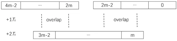
From the equation (3.1), we can get that the partial polynomials AHBHx2m,
{[(AH +AL)(BH +BL)]−[AHBH +ALBL]}xm and ALBL are XORed by adding coefficients of common exponents ofx together. The VLSI module used to perform
this XOR operation is called overlap module [14]. In order to explain overlaps of
common exponents ofx clearly, we present the following table, which shows ranges
of x’s exponents in these three polynomials. From the figure, it is easy to know
Figure 3.1: Ranges ofx’s exponents of equation (3.1)
that overlaps occur only whenn>4 or m>2, and there is no overlap whenn= 2
orm = 1.
Because of the overlaps, one more XOR gate delay is needed in the overlap module
to compute the summation of the three polynomialsAHBHx2m,{[(AH+AL)(BH+
BL)]−[AHBH +ALBL]}xm and ALBL. According to this, a total of 3 XOR gates delays are required in (3.1) besides the cost of the recursive computation of the
three partial products.
Therefore, a new method focus on overlaps has been proposed. Instead of splitting
two input operands int the ”most significant half” and the ”least significant half”,
An Overview of Bit-Parallel Multiplication for GF(2n) and Comparison 18
can rewrite A and B as follows [12]:
A=
n−1
X
i=0
aixi = m−1
X
i=0
a2ix2i + m−1
X
i=0
a2i+1x2i+1 =
m−1
X
i=0
a2ix2i+x m−1
X
i=0
a2o+1x2i
B=
n−1
X
i=0
bixi = m−1
X
i=0
b2ix2i+ m−1
X
i=0
b2i+1x2i+1 =
m−1
X
i=0
b2ix2i+x m−1
X
i=0
b2o+1x2i
Now let y=x2, then operandsA and B can be rewritten as
A=Ae(y) +xAo(y)
B=Be(y) +xBo(y),
where Ae(y) = P m−1
i=0 a2iy
i, A
o(y) = P m−1
i=0 a2i+1y
i, and B
e(y) and Bo(y) are
de-fined similarly. BecauseAe(y),Ao(y),Be(y) andBo(y) are polynomials in degree of
y, which is less thanm, multiplication operations among them may also be
com-puted recursively. Then we can get the product of A, B as the KOA-like formula
as follows
AB= (Ae(y) +xAo(y))(Be(y) +xBo(y))
={Ae(y)Be(y) +x2Ao(y)Bo(y)}+x{Ae(y)Bo(y) +Ao(y)Be(y)} ={Ae(y)Be(y) +yAo(y)Bo(y)}+
x{(Ae(y) +Ao(y))(Be(y) +Bo(y))−(Ae(y)Be(y) +Ao(y)Bo(y))} (3.3)
Obviously, function (3.3) also includes three partial products and in hardware
im-plementation multiplying a polynomial by x or y = x2 is equivalent to shifting
its coefficients left and no extra gate is required. It is clearly to check that the
expansion of Ae(y)Be(y) +yAo(y)Bo(y) contains with even exponents x, and the
expansion ofx{(Ae(y) +Ao(y))(Be(y) +Bo(y))−(Ae(y)Be(y) +Ao(y)Bo(y)) con-tains with odd exponents x. Therefore, no overlap exists when computing their
Consequently, the recurrence relations describing the time and space complexities
can be cited as follows:
S⊗(2) = 3
S⊗(n) = 3S⊗(n2)
T⊗(2) = 1
T⊗(n) =T⊗(n2)
S⊕(2) = 4
S⊕(n) = 3S⊕(n2) + 4n−4
T⊕(2) = 2
T⊕(n) =T⊕(n2) + 2
Then we can get the solutions as below:
S⊕(n) = 6nlog23−8n+ 2
S⊗(n) =nlog23
T⊕(n) = 2 log2n
T⊗(n) = 1
(3.4)
Compared with formula (3.2), the overlap-free method reduces the XOR gate delay
T⊕(n) from 3 log2n−1 to 2 log2n, which nearly equal to 33% forn= 2t (t >1).
3.3
Reconstructed Karatsuba Algorithm
In 2009, Bernstein [15], Zhou and Michalik [16] has optimize the reconstruction
part of the Karatsuba formula by factorizing some constant common terms.
Bern-stein also applied this optimization to the reconstruction of Karatsuba formula
and then to two recursion of Karatsuba resulting in 5.46nlog2(n) +S
⊕ instead of
6nlog2(n)+S⊕ for the original Karatsuba formula and a delay of 2.5 log
2(n)T⊕+T⊗.
Let consider two degreen−1 polynomialsA(x) =Pn−1
i=0 aixiandB(x) =
Pn−1
i=0 bixi
An Overview of Bit-Parallel Multiplication for GF(2n) and Comparison 20
expressing the product C=A×B in terms of three multiplications of polynomial of half size. The detailed computations are given below:
• Component polynomial formation(CPF). The CPF consists of splittingAin
two halves
A(x) = n 2−1
X
i=0
aixi
| {z } AL
+xn2 n 2−1
X
i=0
ai+n2xi
| {z } AH
and then generate three polynomials of half sizeA00 =AL,A
0
1 =AL+AH and
A02 =AH. The same asB =BL+BHx n
2, we generateB
0
0 =BL,B
0
1 =BL+BH
and B02 =BH.
• Recursive products. We perform the pairwise products of the CPF ofA and
B
C00 =A00B00 =ALBL
C01 =A01B01 = (AL+AH)(BL+BH) (3.5)
C02 =A02B02 =AHBH
• Reconstruction. We reconstruct C=A×B as
C=C00(1 +xn2 +C
0
1x
n
2 +C
0
2x
n
2(1 +x
n 2)
=C00+ (C00 +C10 +C02)xn2 +C
0
2xn (3.6)
The three half size products C00, C01 and C02 of (3.5) are computed by applying the same method recursively. If the recursive computations are performed in
parallel we get a parallel multiplier with a sub-quadratic space complexity and a
gates , the total delay shows as below:
S⊗= 6nlog2(3)−8n+ 2
S⊕=nlog2(3)
T= 3 log2(n)T⊕+T⊗
(3.7)
3.4
Improved Reconstruction by Bernstein
Recently an optimized version of the Karatsuba formula, which we mentioned on
previous section, have been proposed. Bernstein have reduced the complexity of
the reconstruction step as follows [18]
Step 1. R0 =P0+x
n
2P1 (Cost = n
2 −1 bit additions)
Step 2. R1 =R0(1 +x
n
2) (Cost =n−1 bit additions) Step 3. C=R1+P2x
n
2 (Cost =n−1 bit additions)
(3.8)
This method reduces the number of bit additions of one recursion of the Karatsuba
formulaS⊕ = 7n/2−3+3S⊕(n/2), which gives for a full recursionS⊕ = 5.5nlog2n− 7n+3/2. But this method converses a delay ofT= 3 log2nD⊕+T⊗. In this result,
we call the reconstruction formula (3.8) as improved reconstruction by Bernstein.
3.5
Comparison
From the previous sections, we have summarized four different kinds of bit-parallel
multiplication algorithms,including original KOA, overlap-free KOA,
reconstruc-tion Karatsuba and improved reconstrucreconstruc-tion by Bernstein. Therefore, we collect
all these four algorithms results and briefly make a comparison, including space
complexity (the number of AND gates and XOR gates)and time complexity. It
An Overview of Bit-Parallel Multiplication for GF(2n) and Comparison 22
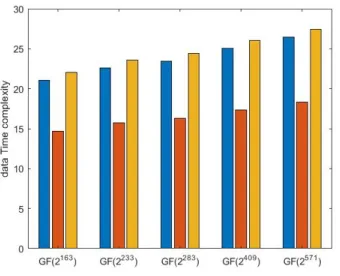
Figure 3.2: Comparison time and space complexities of four different
multi-plication algorithms
set several examples of these four architectures later on NIST(National Institute
of Standard and Technology) recommended fields. The corresponding time and
space complexities and their comparison are given as well. Each kind of algorithm
is applied to build efficient polynomial multiplication over NIST recommended
fields GF(2163), GF(2233), GF(2283) and GF(2409). Some detailed number of the
time and space complexities will also be presented.
First, according to figure 3.2, we analyse the data in horizon direction, which means
that we compare three concepts among four multiplication algorithms, including
#AND (the number of AND gates), #XOR (the number of XOR gates) and time
complexity.
where we use blue, orange and yellow column to represent #AND, #XOR and
time complexity, respectively.
From figure 3.3 we can achieve some disciplines:
• All the methods have approximately same number of AND gates
• Using the Improved Reconstruction by Bernstein algorithm can achieve low-est number of XOR gates
Figure 3.3: Horizon direction comparison
Because of the number of AND gates, we only make the vertical comparison two
concepts among these four algorithms, including #XOR and time complexity.
where red and blue column represent the Improved Reconstruction by Bernstein
Figure 3.4: Comparison in the number of XOR gates
An Overview of Bit-Parallel Multiplication for GF(2n) and Comparison 24
From figure 3.4 we can obtain that
• Improved Reconstruction by Bernstein multiplication algorithm only reduce slight number of XOR gates. The gap between Improved Reconstruction by
Bernstein multiplication algorithm and others may obvious with n
increas-ing.
Figure 3.5: Comparison in time complexity
where blue, red and yellow column represent the original KOA, Overlap-free
Karat-suba and Reconstruction KaratKarat-suba (or Improved Reconstruction by Bernstein),
respectively.
From figure 3.5 we can read that
• The apparent gap between Overlap-free Karatsuba and other three algo-rithms always exists no matter how the value ofn changing.
Above these figures and analyses, we can settle that we will just focus on the
Overlap-free Karatsuba algorithm and its hardware implement in the following
chapters in this thesis. Although the Improved Reconstruction by Bernstein
gates, this result is the consequence of the huge value of m. For the limit of
the input and output number in the FPGA (Field- Programmable Gate Array)
board, which will be mentioned in the next chapter, we will design the hardware
implementation when n = 128. And in this case, the Improved Reconstruction
by Bernstein algorithm does not have a better layout in the comparison of the
number of XOR gates. Therefore, we only do the research on Overlap-free
Karat-suba multiplication algorithm as the following chapter. We will also compare the
proposed hardware implementation with other methods or other published data
Chapter 4
Proposed Hardware
Implementation of Modified
Overlap-free Karatsuba
Multiplication Algorithm for
GF
(2
n
)
In this chapter, we first introduce the fundamental technology information,
includ-ing FPGA and its internal architecture, Verilog HDL and ISE software in detail.
Then we illustrate the meaning of each code correspond to its function in
algo-rithm. Finally, we compare the proposed module implementation with published
article in GF(24), GF(28) and GF(216) and then achieve a considerable result.
4.1
Fundamental Technology Background
In this section, we briefly introduce the fundamental technology that we need
throughout hardware implementation. First, we present what is FPGA and its
internal architecture. In order to program it, we explain the reason why we choose
Verilog as HDL and ISE as the simulator.
4.1.1
FPGA and their internal architecture
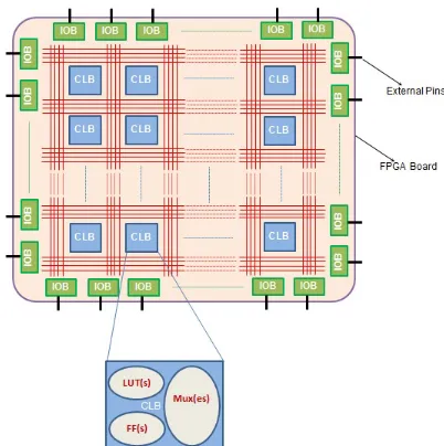
Field Programmable Gate Array (FPGAs) are semiconductor devices that are
based around a matrix of configurable logic blocks (CLBs) connected via
pro-grammable interconnects [19]. Typical internal structure of FPGA (figure 4.1)
comprises of three major elements:
Figure 4.1: Internal architecture of a typical FPGA
• Configurable logic blocks (CLBs), shown as blue boxes in figure 4.1, are the resources of FPGA meant to implement logic functions. Each CLB is
comprised of a set of slices which are further decomposable into a definite
Proposed Hardware Implementation of Modified
Overlap-free Karatsuba Multiplication Algorithm for GF(2n) 28
• Input/Output Blocks (IOBs) available at FPGA’s periphery facilitate ex-ternal connections. These programmable blocks carry signals ’to’ or ’from’
FPGA chip. Figure 4.1 shows IOBs as a set of rectangular boxes enclosed
within the FPGA boundary.
• Switch Matrix, shown as red-coloured lines in figure 4.1, is an interconnecting wire-like arrangement within FPGA. These offer connectivity for the CLBs
or provide dedicated low impedance, minimum delay path such as global
clock line [20].
In general, FPGAs are more flexible than ASICs as they are able to programmed
easily to desired functions or applications, with the emphasis on the ease of
re-programmability. This is the feature that makes such devices suitable for building
processing units for polynomials which are likely to have to adapt to parameter
changes from time to time. The fundamental building block of a FPGA is its logic
cells. Despite the different hardware used to realize the logic cell functions and
different input widths provided by various FPGA vendors, they can be mapped
to certain logic functions with the help of the synthesis and mapping tools.
Xilinx Spartan-605 FPGA cells contain a 6-input LUTs improving performance
and minimize power in a certain degree. Each CLB in Spartan-605 FPGA
con-sists of two slices, arranged side-by-side as part of two vertical columns. There are
three types of CLB slices in the Spartan-605 architecture: SLICEM, SLICEL and
SLICEX. Each slice contains four LUTs, eight FFs, and miscellaneous logic. The
LUTs are for general-purpose combinatorial and sequential logic support.
Syn-thesis tools take advantage of these highly efficient logic, arithmetic and memory
4.1.2
Verilog HDL and ISE Design Suite
FPGAs are much more than just a bunch of gates. Although it is possible to build
logic circuits of any complexity simply by arranging and connecting logic gates, it
is just not practical and efficient. So we need a way to express the logic in some
easy to use format that can be converted to an array of gates eventually. And
HDL will be focused throughout this thesis. A Hardware Description Language
(HDL) is a software programming language used to model the intended operation
of a piece of hardware. There are two aspects to the description of hardware
that an HDL facilities; the abstract behaviour modelling and hardware structure
modelling.
• Abstract behaviour modelling. A hardware description language is
declar-ative in order to facilitate the abstract description of hardware behaviour
for specification purposes. This behaviour is not prejudiced by structural or
design aspects of the hardware intent.
• Hardware structure modelling. Hardware structure is capable of being
mod-elled in a hardware description language irrespective of the design’s
be-haviour.
The behaviour of hardware may be modelled and represented at various levels of
abstraction during the design process. Higher level models describe the
opera-tion of hardware abstractly, while lower level models include more detail, such as
inferred hardware structure.
Verilog, standardized as IEEE 1364, is a HDL, which can be used to describe
digital circuits in a textual manner [23]. It is most commonly used in the design
and verification of digital circuits at the register transfer level (RTL) of abstraction.
It is also used in the verification of analog circuits and mixed-signal circuits, as
well as in the design of genetic circuits. Verilog gained a strong foothold among
Proposed Hardware Implementation of Modified
Overlap-free Karatsuba Multiplication Algorithm for GF(2n) 30
• The behavioural constructs of Verilog could describe both hardware and test stimulus.
• The Verilog simulator is fast, especially at the gate level.
• The Verilog simulator is an ”interpreter”, which interpretive software ex-ecutes source code directly instead of pre-compiling the source code into
intermediate ”object” code.
According to these features, we choose Verilog as HDL in this thesis to write the
code and program the FPGA board.
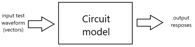
Simulation is the fundamental and essential part of the design process for any
electronic based product; not just FPGA devices. For FPGA devices, simulation
is the process of verifying the function characteristics of models at any level or
behaviour, that is, from high levels of abstraction down to low levels. The basic
arrangement for simulation is shown in Figure 4.2.
Figure 4.2: Basic simulation arrangement
In this thesis, we choose Xilinx ISE software as the simulator to finish the FPGA
board hardware simulation. The Xilinx ISE (Integrated Synthesis Environment)
produced by Xilinx for synthesis and analysis of HDL design. The ISE software
controls all aspects of the design flow [24]
• perform timing snaysis
• examine RTL diagrams
• simulate a design’s reaction to different stimuli
• configure the target device with the programmer
Through the Project Navigator interface (shown in figure 4.3), you can access all
Figure 4.3: Project Navigator Interface [24]
of the design entry and design implementation tools. You can also access the files
and documents associated with your project.
4.2
Hardware implementation of Modified
Overlap-free Karatsuba algorithm for
GF
(2
n)
on FPGA
In this section, we first present the complexity analysis by applying 1-step
Overlap-free KA (Karatsuba) for even-term polynomials (ETP). Then we apply the
Proposed Hardware Implementation of Modified
Overlap-free Karatsuba Multiplication Algorithm for GF(2n) 32
4.2.1
Fundamental Multiplication Modules for
GF
(2
4)
We now convey an example to compare the proposed modified method with the
original KOA. We assume n= 4 and then let
A=a3x3+a2x2+a1x+a0 =AHx2+AL
B=b3x3+b2x2 +b1x+b0 =BHx2+BL
where AH = a3x+a2, AL = a1x+a0, BH =b3x+b2 and BL = b1x+b0 are the
polynomials of degree 1 in x. Then the original KOA computes the product AB
using
AB=AHBHx4+{[(AH +AL)(BH +BL)] + [AHBH +ALBL]}x2+ALBL (4.1)
there are three products of polynomials of degree 1 in (4.1), and they can be
computed recursively using the KOA at a cost of 2Tx.
To show the role of the overlap in 4.1, we group the three products in 4.1 and
write them as polynomials of degree 2 in x as follows:
d2x2 +d1x+d0 = AH +BH
e2x2 +e1x+e0 = [(AH +AL)(BH +BL)] + [AHBH +ALBL]
f2x2+f1x+f0 = ALBL
Then we have
AB = (d2x2+d1x+d0)x4+ (e2x2+e1x+e0)x2+ (f2x2+f1x+f0)
= d2x6+d1x5+ (d0+e2)x4 +e1x3 + (e0+f2)x2 +f1x+f0 (4.2)
Obviously, one XOR gate delay 1Txis required to compute the overlap summations
the curly bracket of (4.1), the total number of XOR gate delays of the original
KOA is 2 + 1 + 2 = 5.
Let y= x2, the proposed method in Chapter 2 function computes AB as follows
[13]
AB= (Ae(y) +xAo(y))(Be(y) +xBo(y))
={Ae(y)Be(y) +x2Ao(y)Bo(y)}+x{Ae(y)Bo(y) +Ao(y)Be(y)} ={Ae(y)Be(y) +yAo(y)Bo(y)}+
x{(Ae(y) +Ao(y))(Be(y) +Bo(y))−(Ae(y)Be(y) +Ao(y)Bo(y))} (4.3)
where Ae(y) =a2y+a0,Ao(y) =a3y+a1, Be(y) =b2y+b0 and Bo(y) =b2y+b1
are polynomials of degree 1 in y, where we will do modified into the architecture.
Then we define four polynomials of degree 2 iny as belows:
p2y2+p1y+p0 = Ae(y)Be(y)
q2y2+q1y+q0 = Ao(y)Bo(y)
r2y2+r1y+r0 = (Ae(y) +Ao(y))(Be(y) +Bo(y))
s2y2+s1y+s0 = Ae(y)Be(y) +Ao(y)Bo(y)
We need 1Tx to perform ”+” operations in the last two equations. We also need
2Tx to compute the three products of polynomials of degree 1 in yin the above
four equations. Then we have the product AB can be shown as follows:
AB={(p2y2+p1y+p0) +y(q2y2+q1y+q0)}+
x{(r2y2+r1y+r0) + (s2y2+s1y+s0)}
=q2x6+ (p2+q1)x4+ (p1+q0)x2+p0+
(r2+s2)x5+ (r1+s1)x3+ (r0+s0)x
Proposed Hardware Implementation of Modified
Overlap-free Karatsuba Multiplication Algorithm for GF(2n) 34
Evidently, one XOR gate delay is needed to obtain the summations in the five
brackets. Therefore the total number of XOR gate delay is 4, and 1Tx has been
saved compared to the original KOA.
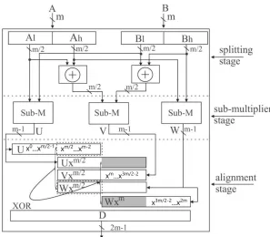
Figure 4.4 shows the multiplier architecture by applying one step Overlap-free KA
algorithm as above example, ifm=nis even. The multiplier includes three stages:
the splitting stage, the sub-multiplier stage and the alignment stage, where three
sub-multiplier operate in parallel.
Figure 4.4: Multiplier Architecture by applying Overlap-free KA
In this architecture [16], we can efficiently define which part’s function. The
split-ting stage requires m XOR gates to generate the inputs for the middle multiplier,
which compute the product of Ae(y) +Ao(y) and Be(y) +Bo(y). The alignment
stage merges the output of sub-multipliers according to their degrees. Both in
and Dm...3m
2 −2 [25]
Dm
2...m−2 = [U m
2...m−2+W0... m
2−2] +U0... m
2−2+V0... m
2−2
Dm...3m
2 −2 = [U
m
2...m−2+W0... m
2−2] +W
m
2...m−2+V m
2...m−2
(4.5)
Using this architecture and proposed modified Overlap-free Karatsuba algorithm,
we can implement it on the typical FPGA board and analyse its features.
4.2.2
Implementation of proposed modified algorithm
for
GF
(2
n)
on FPGA
In this part, we will combine the proposed modified Overlap-free KA algorithm
with the Multiplier architecture, and use Verilog HDL to complete the
implementa-tion of proposed modified Overlap-free KA algorithm for GF(2n), where n= 128,
on Xilin Spartan-605 board.
In order to make easier understand, we first make the module when n = 2 as an
example. The detail Verilog HDL code has been shown in table 4.1.
Table 4.1: Verilog HDLn= 2 module
1 m o d u l e m u l _ 2 _ m o d u l e ( 2 i n p u t [ 1 : 0 ] A , 3 i n p u t [ 1 : 0 ] B , 4 o u t p u t [ 3 : 0 ] m u l _ 2 5 );
6 a s s i g n m u l _ 2 [ 0 ] = A [ 0 ] & B [ 0 ] ; 7 a s s i g n m u l _ 2 [ 2 ] = A [ 1 ] & B [ 1 ] ; 8 a s s i g n m u l _ 2 [ 3 : 0 ] =
9 { A [ 1 ] & B [1] ,
10 ( A [ 0 ] ^ A [ 1 ] ) & ( B [ 0 ] ^ B [ 1 ] ) ^ m u l _ 2 [ 0 ] ^ m u l _ 2 [2] , A [ 0 ] & B [ 0 ] } ; 11 e n d m o d u l e
Because of the value of n, in Chapter 3 we have mentioned, no overlap will occur
at this time. To analyse the table 4.1 more clearly, we show some typical steps
Proposed Hardware Implementation of Modified
Overlap-free Karatsuba Multiplication Algorithm for GF(2n) 36
a s s i g n m u l _ 2 [ 0 ] = A [ 0 ] & B [0]
equal to function ALBL
a s s i g n m u l _ 2 [ 2 ] = A [ 1 ] & B [1]
equal to function AHBH
a s s i g n A [ 0 ] ^ A [ 1 ] ) & ( B [ 0 ] ^ B [ 1 ] ) ^ m u l _ 2 [ 0 ] ^ m u l _ 2 [2]
equal to function [(AH +AL)(BH +BL)] + [AHBH +ALBL]
Then we extend the value ofn from 2 to 4, which Verilog HDL shows in table 4.2.
Since value 4 is exact double size of 2, we use nested and transferred statement to
finish the module. For this value, overlap occurs during the alignment stage and
then we apply the proposed algorithm in this part, which also shows in the table
4.2, the specific code as below:
a s s i g n d7 = d2 ^ d1 ^ d0 ;
a s s i g n m u l _ 4 [ 7 : 0 ] = { d2 [3:2] ,( d2 [ 1 : 0 ] ^ d7 [3:2]) ,
( d0 [ 3 : 2 ] ^ d7 [1:0]) , d0 [ 1 : 0 ] }
therefore, we can extend the value of n until 128. The detail Verilog HDL code
has been shown in Appendix in the end of this thesis.
Table 4.2: Verilog HDLn= 4 module
1 m o d u l e m u l _ 4 _ m o d u l e ( 2 i n p u t [ 3 : 0 ] A ,
3 i n p u t [ 3 : 0 ] B , 4 o u t p u t [ 7 : 0 ] m u l _ 4 5 );
6 w i r e [ 3 : 0 ] d0 , d1 , d2 , d7 ;
7 m u l _ 2 _ m o d u l e u0 (( A [ 1 : 0 ] ) , ( B [ 1 : 0 ] ) , ( d0 ));
8 m u l _ 2 _ m o d u l e u1 (( A [ 1 : 0 ] ^ A [ 3 : 2 ] ) , ( B [ 1 : 0 ] ^ B [ 3 : 2 ] ) , ( d1 )); 9 m u l _ 2 _ m o d u l e u2 (( A [ 3 : 2 ] ) , ( B [ 3 : 2 ] ) , ( d2 ));
10 a s s i g n d7 = d2 ^ d1 ^ d0 ;
11 a s s i g n m u l _ 4 [ 7 : 0 ] = { d2 [3:2] ,( d2 [ 1 : 0 ] ^ d7 [3:2]) , 12 ( d0 [ 3 : 2 ] ^ d7 [1:0]) , d0 [ 1 : 0 ] } ;
13 e n d m o d u l e
Following the nested and transferred statement, we finally get the module of n=
the simulation of all the huge module. From the simulator, we first implement
this module in to the typical board, Xilinx Spartan-605. And then complete
implement design part, including translate, map and place & route. After that,
we also generate programming file and from the simulation part, we achieve the
RTL schematic in figure 4.5.
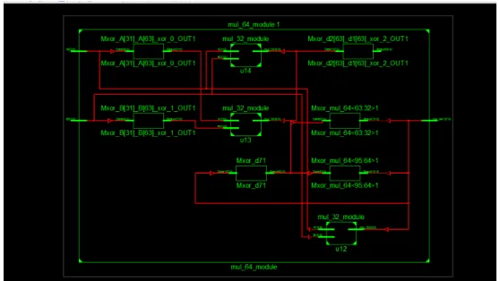
Figure 4.5: RTL Schematic
In figure 4.5, we can directly know that our module exactly follows multiplier
architecture, in figure 4.4. There are several CLBs shown in the RTL scheme,
including the input, output and the name of the block, which also illustrates the
steps.
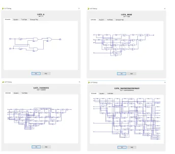
In each CLB, when we check in it, it shows the kinds of LUTs, FFs and MUX. And
we summarise the exact kinds of LUTs, in figure 4.6 which occurs in the whole
module.
Internally, LUTs comprises of 1-bit memory cells and a set of multiplexers. One
value among these SRAM bits will be available at the LUT’s output depending
on the value(s) fed to the control line(s) of the multiplexers. For these features,
LUTs is an important cell in CLB. If we can design the LUT’s structure, we may
optimize the speed of input and output, which reflects on chips is the speed of
Proposed Hardware Implementation of Modified
Overlap-free Karatsuba Multiplication Algorithm for GF(2n) 38
Figure 4.6: 2, 4, 5 and 6-input LUTs
We can also get ISm simulation in the simulator, shown in figure 4.7 and 4.8
without and with input respectively. We can control the value of each input,
directly achieve the output value, analyse the time delay and get wave changes if
we design the clockwise.
Figure 4.7: ISim simulation without input module
In the next section, we will discuss the time delay and the comparison value of
Figure 4.8: ISm simulation with proposed input module
4.3
Complexity Comparison
In this section, we first present the simulation results of proposed modified module
in Verilog code and ISE system. Then compare it with other published multipliers,
for GF(24),GF(28) and GF(216) field, referencing specific paper.
4.3.1
Synthesis results
First, we take the simulation results of proposed modified module using
overlap-free Karatsuba multiplication algorithm forGF(24) as an example, which has been
shown in following codes and figures.
The proposed modified module has been coded in Verilog in Appendix B. From the
code, the first two inputs have been settled 001, 001 respectively and the system
needs to wait 100ns for global reset to finish. Then the value of B, which is one of
inputs, has changed from 001 to 111 every 1ns. And using the simulation system
we can achieve the following figure.
The figure shows the binary equivalent of multiplication of two 4-bit numbers to
give the product. Ports A and B are the input ports that accept the numbers
to be multiplied. The port mul 4 is the output port, where the product of the
two aforesaid numbers are obtained. For example, the product of 0001 and 0001
(binary equivalents), specified at the ports A and B respectively, is obtained at
Proposed Hardware Implementation of Modified
Overlap-free Karatsuba Multiplication Algorithm for GF(2n) 40
Figure 4.9: Simulation result of proposed modified module for GF(24)
fieldGF(28) andGF(216) are obtained, shown as figure 4.10 and 4.11 respectively.
Figure 4.10: Simulation result of proposed modified module for GF(28)
Figure 4.11: Simulation result of proposed modified module for GF(216)
4.3.2
Comparison
According to the simulation results, we reference the paper called FPGA Based
Modified Karatsuba Multiplier [32] because it has valuable kinds of finite field
multipliers. We have studied the performance of each multiplier over GF(24),
are implemented on Spartan-605 device. These multipliers are compared based on
number of slices, 4-input LUTs, bonded I/O blocks and maximum combinational
path delay.
Figure 4.12: Comparison of device utilization and combinational path delay
of proposed modified multipliers and other multipliers for GF(24)
Table in figure 4.12 shows the result of device utilization and combinational path
delay of various types of GF(24) multipliers. The number of slices and
combina-tional path delay for proposed modified multiplier are 6 out of 6822 and 10.101 ns
respectively. Whereas, the minimum number of slices and combinational path
de-lay for Modified Karatsuba multiplier are 6 out of 6822 and 13.057 ns respectively.
Although they have the same number of slices, the combinational path delay for
proposed modified multiplier is 23.4% lower than the one for Modified Karatsuba,
which is the minimum combinational path delay among the other multipliers.
In order to make the comparison clearer, we only implement the polynomial
mul-tiplication part, which will be research further in Chapter 5. So we compare
Karatsuba, Modified Karatsuba and proposed modified Overlap-free algorithm
multiplication, in the following comparison for GF(28) and GF(216).
Tables 4.3 and 4.4 illustrate the result of device utilization and combinational path
delay of three types multipliers for GF(28) and GF(216) respectively. The
Proposed Hardware Implementation of Modified
Overlap-free Karatsuba Multiplication Algorithm for GF(2n) 42
Table 4.3: Comparison of device utilization and combinational
path delay forGF(28)
Different No. of slices No.of 4-input No.of boned Max
GF (out of 6822) LUTs IOBs combinational
Multipliers (out of 27288) (out of 296) path delay(ns)
Karatusba[31] 66 115 24 20.028
Modified 36 62 24 17.035
Karatsuba[32]
Proposed modified 60 74 24 13.425
Overlap-free
Table 4.4: Comparison of device utilization and combinational
path delay forGF(216)
Different No. of slices No.of 4-input No.of boned Max
GF (out of 6822) LUTs IOBs combinational
Multipliers (out of 27288) (out of 296) path delay(ns)
Karatusba[31] 252 395 52 27.012
Modified 130 230 52 24.413
Karatsuba[32]
Proposed modified 248 254 52 18.277
Overlap-free
ns and 18.277 ns respectively. For GF(28), the combinational path delay for
pro-posed modified Overlap-free multiplier is 32.97% lower than that for Karatsuba
multiplier and 21.19% lower than the one for Modified Karatsuba multiplier. For
GF(216), the combinational path delay for proposed modified Overlap-free
multi-plier is 32.34% and 25.13% lower than that for Karatsuba multiplier and Modified
Karatsuba multiplier respectively. Although the number of slices occupied of
pro-posed modified Overlap-free multiplier is not obviously less than the other two
methods, the max combinational path delay of proposed modified Overlap-free
multiplier has a significant reduction among these three methods.
In conclusion, proposed modified multiplier module has less hardware space
com-plexity and time comcom-plexity than other finite field multipliers. And this result
multiplication has lower time delay comparing with other kinds of finite field
Chapter 5
Conclusion
In this chapter, we summarize the main contribution in this thesis and propose
the future work in related implementation.
5.1
Summary of Contribution
Bit-parallel multiplication applied with modified Overlap-free Karatsuba
algo-rithm has been investigated in this thesis when n is presented for NIST
recom-mended fields. Our main contribution is summarized as follows:
• Compared Overlap-free Karatsuba algorithm with other existing popular algorithm, such as Karatsuba algorithm, reconstruction Karatsuba algorithm
and improved reconstruction by Bernstein, and achieve the advantage of
proposed algorithm in the max combinational path delay.
• Implement the proposed modified Overlap-free Karatsuba algorithm multi-plication on FPGA board, simulate in the ISE Xilinx system and achieve
the synthesis result in NIST recommended field n= 128.
• Compared proposed modified Overlap-free Karatsuba algorithm multipli-cation with especially published multiplimultipli-cations (Karatsuba and Modified
Karatsuba multiplications),forGF(24),GF(28) andGF(216). The results of
the comparison have confirmed that proposed modified Overlap-free
Karat-suba algorithm multiplication provides a obvious reduction on the max
com-binational path delay.
5.2
Future Work
Proposed modified Overlap-free Karatsuba algorithm multiplication effects the
most research efforts on parallel finite field multiplications. In this thesis, it talks
about multiplication part of a bit-parallel polynomial basis multiplier without
the reduction modulo of the irreducible polynomial. So the potential work will
discusses implementation of the irreducible polynomial.
There are two steps to implement a bit-parallel polynomial basis multiplier in
GF(2n): polynomial multiplication and reduction modulo [33]. In this thesis, we
finish the first step, and define that proposed modified Overlap-free Karatsuba
algorithm polynomial multiplication is the best in critical path among the other
methods. In the optimization work, to make this result more persuasive, we will
choose a irreducible polynomial to reduce modulo in the result of A(x) and B(x) productionD(x). The most significantm−1 terms ofD(x) are iteratively reduced to polynomials with degree less than m by using the irreducible polynomial F(x)
[25]. The reduction operation usually costs a small number of gates compared
with KOMs because F(x) typically has low weight as recommended by the NIST
in [34] and the SECG in [35]. So adding the reduction modulo, will not effect the
Bibliography 46
Table 5.1: Complexity for modular reduction operations[25]
m 113 128 163 193 233 283 # XOR 232 527 665 398 537 1159
Table 5.1 shows the number of XOR gates for the finite field with the irreducible
given in equation 5.1.
GF(2113) :F(x)
113 =x113+x9+ 1
GF(2128) :F(x)
128 =x128+x8+x7+x2 +x+ 1
GF(2163) :F(x)
163 =x163+x7+x6+x3 + 1
GF(2193) :F(x)
193 =x193+x15+ 1
GF(2233) :F(x)
233 =x233+x74+ 1
GF(2283) :F(x)
283 =x283+x12+x7+x5+ 1
(5.1)
F(x)128 is adopted for GHASH function in the AES-GCM standard [36], and other
polynomials are recommended for elliptic curve crypto-systems by NIST
FIPS-186-2 standard [34] or the SECG domain parameters in [35].
In conclusion, the future work implementation of proposed modified Overlap-free
Karatsuba algorithm multiplication for GF(2n), where n = 128, can be
concur-rently applied polynomial multiplication and reduction modulo with the function

![Figure 4.3: Project Navigator Interface [24]](https://thumb-us.123doks.com/thumbv2/123dok_us/1498848.1183527/42.596.199.432.282.458/figure-project-navigator-interface.webp)