Reducing the Area of A Chip Using QCA with
X-Bit × 32-Bit SRAM
Inba Manimegalai.J, P.Priya Dharsini
PG Student, Department of ECE, Rajas Engineering College, Raja Nagar, Vadakkangulam, Tamil Nadu, India
Assistant Professor, Department of ECE, V.V College of Engineering, Tisayanvillai, Tamil Nadu, India
ABSTRACT: Application of quantum-dot cellular automata (QCA) technology as an alternative to CMOS technology on the nano scale has a promising future; QCA is an interesting technology for building memory. The proposed design and simulation of a new memory cell structure based on QCA with a minimum delay, area, and complexity is presented to implement a static random access memory (SRAM). My project presents the design and simulation of a 16-bit × 32-bit SRAM with a new structure in QCA. Since QCA is a pipeline, this SRAM has a high operating speed. The 16-32-bit × 32-bit SRAM has a new structure with a 32-bit width designed and implemented in QCA. It has the ability of a conventional logic SRAM that can provide read/write operations frequently with minimum delay. The 16-bit × 32-bit SRAM is generalized and an n × 16-bit × 32-bit SRAM is implemented in QCA. Novel 16-bit decoders and multiplexers (MUXs) in QCA are presented that have been designed with a minimum number of majority gates and cells. The new SRAM, decoders, and MUXs are designed, implemented, and simulated in QCA using a signal distribution network to avoid the coplanar problem of crossing wires. The QCA-based SRAM cell was compared with the SRAM cell based on CMOS. Results show that the proposed SRAM is more efficient in terms of area, complexity, clock frequency, latency, throughput, and power consumption.
I. INTRODUCTION
1.1 Landauer Clocking for Magnetic Cellular Automata (MCA) Arrays
Magnetic cellular automata (MCA) is a variant of quantum dot- cellular automata (QCA) where neighboring single-domain nano magnets also termed as magnetic cell process and propagate information logic 1 or logic 0 through mutual interaction. The attractive nature of this framework is that not only room temperature operations are feasible but also interaction between neighbors is central to information processing as opposed to creating interference. In this work, we explore spatially moving Landauer clocking scheme for MCA arrays length of 8, 16, and 32 cells and show the role and effectiveness of the clock in propagating logic signal from input to output without magnetic frustration. Simulation performed in object oriented micro magnetic framework suggests that the clocking field is sensitive to scaling, shape, and aspect ratio.
1.2 Area-Delay Efficient Binary Adders in QCA
As transistors decrease in size more and more of them can be accommodated in a single die, thus increasing chip computational capabilities. However, transistors cannot get much smaller than their current size. The quantum-dot cellular automata (QCA) approach represents one of the possible solutions in overcoming this physical limit, even though the design of logic modules in QCA is not always straightforward.Quantum-dot cellular automata (QCA) are an attractive emerging technology suitable for the development of ultra-dense low-power high-performance digital circuits. For this reason, in the last few years, the design of efficient logic circuits in QCA has received a great deal of attention. Special efforts are directed to arithmetic circuits, with the main interest focused on the binary addition that is the basic operation of any digital system.
1.3 Thermal Switching Error versus Delay Tradeoffs in Clocked QCA Circuits:
circuit.This clocking scheme, however, induces latency or delay in the transmission of information from input to output. The interplay of computing error behavior with delay or latency of computation induced by the clocking scheme.Computing errors in QCA circuits can arise due to the failure of the clocking scheme to switch portions of the circuit to the ground state with change in input. Some of these non-ground states will result in output errors and some will not the larger the size of each clocking zone, i.e., the greater the number of cells in each zone, the more the probability of computing errors.
1.4 An NCL-HDL Snake-Clock-Based Magnetic QCA Architecture
The International Technology Roadmap of semiconductors suggests that quantum-dot cellular automata (QCA) technology might be a possible CMOS substitute. In particular, magnetic quantum-dot cellular automata have recently drawn the attention of the researchers. Previous experimental works have demonstrated that MQCA are feasible, and can be fabricated with existing technological processes. They are also attractive due to their compactness and an extremely small power dissipation. Unlike in previous contributions, where architectural blocks are often presented without or only slightly considering their relations with technology, here we conceived, implemented, and described a complex MQCA computational block maintaining a clear link with technology.This link is achieved at different levels. At an architectural level, we propose the use of delay insensitive null convention logic .It is implemented for MQCA in order to solve the “layout=timing” problem in the specific case of MQCA. thus, describe an architectural block at system level using a hardware description language.This NCL-HDL idea is adapted to a new structure, which have called “snake clock,” proposed as a feasible solution for the problem of clock delivery, essential for MQCA operations.
1.5 A Scalable Signal Distribution Network for Quantum-Dot Cellular Automata
A signal distribution network (SDN) for quantum-dot cellular automata (QCA) devices. This network allows the distribution of a set of N inputs to an arbitrary number of combinational functions, overcoming the challenges associated with wire crossings that have faced QCA systems for many years. As an additional benefit, the proposed SDN requires only four distinct clock signals, regardless of the number of inputs or outputs, and those clock signals each repeat a very simple pattern. Furthermore, this network is highly scalable, completing the distribution of N inputs to an arbitrary number of distributed signals and an arbitrary number of outputs in 4N – 2 clock cycles.
1.5 Quantum Dot Cellular Automata Check Node Implementation for LDPC Decoders
The quantum dot Cellular Automata (QCA) is an emerging nanotechnology that has gained significant research interest in recent years. Extremely small feature sizes, ultra low power consumption, and high clock frequency make QCA a potentially attractive solution for implementing computing architectures at the nanoscale. To be considered as a suitable CMOS substitute, the QCA technology must be able to implement complex real-time applications with affordable complexity. Low density parity check (LDPC) decoding is one of such applications.The core of LDPC decoding lies in the check node (CN) processing element which executes actual decoding algorithm and contributes toward overall performance and complexity of the LDPC decoder.
1.6 The Robust QCA Adder Designs Using Composable QCA Building Blocks
Quantum-dot cellular automata (QCA) is attracting a lot of attention due to its extremely small feature size and ultralow power consumption. Up to now, several adder designs using QCA technology have been proposed. However, it was found that not all of the designs function properly. This paper analyzes the reasons of the failures and proposes adders that exploit proper clocking schemes.Scaling of CMOS devices is being aggressively pursued by shrinking transistor dimensions, reducing power supply voltages, and increasing operating frequencies. Such aggressive scaling adversely results in a series of non ideal behaviors such as high leakage current and high power density levels.
1.7 A Serial Memory by Quantum-Dot Cellular Automata (QCA)
memory.The QCA paradigm of memory-in-motion is accomplished using a novel arrangement in the storage loop and timing/clocking; a three- zone memory tile is proposed by which information is moved across a concatenation of tiles by utilizing a two-level clocking mechanism. Clocking zones are shared between memory cells and the length of the QCA line of a clocking zone is independent of the word size. An extensive comparison of the proposed architecture and previous QCA serial memories is pursued in terms of latency, timing, clocking requirements, and hardware complexity.
II. PROPOSED SYSTEM
The proposed design and simulation of a new memory cell structure based on QCA with a minimum delay, area, and complexity is presented to implement a static random access memory (SRAM). This system presents the design and simulation of a 16-bit × 32-bit SRAM with a new structure in QCA. Since QCA is a pipeline, this SRAM has a high operating speed. The 16-bit × 32-bit SRAM has a new structure with a 32-bit width designed and implemented in QCA.
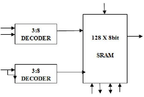
2.1 BLOCK DIAGRAM
Figure 2.1 QCA Architecture
2.2 DECODER
It will convert binary information from n input signals to as many as 2^n unique output signals. Data is transmitted by using Data input the range is 32bit. When the SRAM enables the Read/Write operation is performed.
2.3 SRAM:
RAM is normally associated with volatile types of memory where stored information is lost if power is removed. In SRAM, a bit of data is stored using the state of transistor memory cell. This form of RAM is more expensive to produce, but is generally faster and requires less power than DRAM and, in modern computers, is often used as cache memory for the CPU.
2.4 QCA
merger of elements of both (1) the study of cellular automata in conventional computer science and (2) the study of quantum information processing. In particular, the following are features of models of quantum cellular automata:The computation is considered to come about by parallel operation of multiple computing devices, or cells. The cells are usually taken to be identical, finite-dimensional quantum systems e.g. each cell is a qubit.Each cell has a neighbourhood of other cells. Altogether these form a network of cells, which is usually taken to be regular e.g. the cells are arranged as a lattice with or without periodic boundary conditions.
The evolution of all of the cells has a number of physics-like symmetries. Locality is one: the next state of a cell depends only on its current state and that of its neighbours. Homogeneity is another: the evolution acts the same everywhere, and is independent of time.The state space of the cells, and the operations performed on them, should be motivated by principles of quantum mechanics.
Another feature that is often considered important for a model of quantum cellular automata is that it should be universal for quantum computation i.e. that it can efficiently simulate quantum Turing machines, some arbitrary quantum circuit or simply all other quantum cellular automata.Models which have been proposed recently impose further conditions, e.g. that quantum cellular automata should be reversible and/or locally unitary, and have an easily determined global transition function from the rule for updating individual cells. Recent results show that these properties can be derived axiomatically, from the symmetries of the global evolution. A proposal for implementing classical cellular automata by systems designed with quantum dots has been proposed under the name "quantum cellular automata" by Doug Tougaw and Craig Lent, as a replacement for classical computation using CMOS technology. In order to better differentiate between this proposal and models of cellular automata which perform quantum computation, many authors working on this subject now refer to this as a quantum dot cellular automaton.
2.4.1Standby
If the word line is not asserted, the access transistors M5 and M6 disconnect the cell from the bit lines. The two cross-coupled inverters formed by M1 – M4 will continue to reinforce each other as long as they are connected to the supply.
2.4.2 Reading
In theory, reading process requires only asserting the word line WL and reading the SRAM cell state by a single access transistor and bit line, e.g. M6, BL. Nevertheless bit lines are relatively long with large parasitic capacitance.Therefore to speed-up reading, more complex process is used in practice: The read cycle is started by pre charging by an external module not shown in the figures both bit lines BL and BL, i.e. driving the bit lines to a threshold voltage midrange voltage between logical 1 and 0.Then asserting the word line WL, enabling both the access transistors M5 and M6 which causes that the bit line BL voltage either slightly drops bottom NMOS transistor M3 is ON and top PMOS transistor M4 is off or raises top PMOS transistor M4 is on.It should be noted that if BL voltage rises, the BL voltage drops, and vice versa. Then the BL lines will have a small voltage difference between them while reaching a sense amplifier, which will sense which line has the higher voltage thus determining whether there was 1 stored or 0. The higher the sensitivity of the sense amplifier, the faster the speed of the read operation.
2.4.2 Writing
The start of a write cycle begins by applying the value to be written to the bit lines. If we wish to write a 0, we would apply a 0 to the bit lines, i.e. Setting BL to 1 and BL to 0. This is similar to applying a reset pulse to an SR latch, which causes the flip flop to change state.This is easily obtained as PMOS transistors are much weaker than NMOS when same sized. Consequently when one transistor pair e.g. M3 and M4 is only slightly overriden by the write process, the opposite transistors pair M1 and M2 gate voltage is also changed. This causes that M1 and M2 transistors can be easier over ridden, and so on. Thus, cross-coupled inverters magnify the writing process.
III. CONCLUSION
32 bit. When the SRAM enables the Read/Write operation is performed. If Read operation is performing data is stored in Register. If the Write operation is performing data is get from Register.
REFERENCES
[1] Amlani I., A. O. Orlov, G. Toth, G. H. Bernstein, C. S. Lent, and G. L. Snider, “Digital logic gate using quantum-dot cellular automata,” Science, vol. 284, no. 5412, pp. 289–291, 1999.
[2] Awais M., M. Vacca, M. Graziano, M. R. Roch, and G. Masera, “Quantum dot cellular automata check node implementation for LDPC decoders,” IEEE Trans. Nanotechnol., vol. 12, no. 3, pp. 368–377, May 2013.
[3] Blair E. P., E. Yost, and C. S. Lent, “Power dissipation in clocking wires for clocked molecular quantum-dot cellular automata,” J. Comput. Electron., vol. 9, no. 1, pp. 49–55.
[4] Bhanja S. and S. Sarkar, “Thermal switching error versus delay tradeoffs in clocked QCA circuits,” IEEE Trans. Very Large Scale Integr. (VLSI) Syst., vol. 16, no. 5, pp. 528–541, May 2008
[5] Dehkordi M. A., A. S. Shamsabadi, B. S. Ghahfarokhi, and A. Vafaei, “Novel RAM cell designs based on inherent capabilities of quantum-dot cellular automata,” Microelectron. J., vol. 42, no. 5, pp. 701–708, 2011.
[6] Frost S. E., A. F. Rodrigues, A. W. Janiszewski, R. T. Rausch, and P. M. Kogge, “Memory in motion: A study of storage structures in QCA,” in Proc. 1st Workshop Non-Silicon Comput., 2002, pp. 1–8.
[7] Graziano M., M. Vacca, A. Chiolerio, and M. Zamboni, “An NCL-HDL snake-clock-based magnetic QCA architecture,” IEEE Trans. Nanotechnol., vol. 10, no. 5, pp. 1141–1149, Sep. 2011