ABSTRACT
TUCKER, ERIC ZACHARY. Issues in Patterning Self-Assembled Monolayers by Molecular Replacement: Comparison of Adventitious and Directed Replacement of One Molecule in a SAM with another. (Under the direction of Christopher B. Gorman).
Issues in Patterning Self-Assembled Monolayers by Molecular Replacement: Comparison of Adventitious and Directed Replacement of One Molecule in a SAM with another
by
Eric Zachary Tucker
A dissertation submitted to the Graduate Faculty of North Carolina State University
in partial fulfillment of the requirements for the degree of
Doctor of Philosophy
Chemistry
Raleigh, North Carolina 2011
APPROVED BY:
_______________________________ ______________________________
Dr. Christopher B. Gorman Dr. Edmond Bowden
Chair of the Advisory Committee
DEDICATION
BIOGRAPHY
ACKNOWLEDGMENTS
TABLE OF CONTENTS
LIST OF TABLES ... viii
LIST OF FIGURES ... ix
Chapter 1 - INTRODUCTION ... 1
1.1 Miniaturization of Electronics ... 1
1.2 Scannning Probe Microscopy ... 4
1.3 Alkanethiol Self-assembled Monolayers on Gold ... 9
1.4 Scanning Probe Lithography ... 16
1.5 References ... 31
Chapter 2 - EFFECT OF DEFECTS ON REPLACEMENT LITHOGRAPHY ... 34
2.1 Introduction: Types of Defects in Alkanethiol SAMs on Gold ... 34
2.2 Reducing Defects in SAMs by Vapor Deposition ... 37
2.2.1 Literature Precedent ... 37
2.2.2 Results and Discussion ... 39
2.3 Reducing Defects in SAMs by Thermal Annealing in Air ... 41
2.3.1 Literature Precedent ... 41
2.3.2 Results and Discussion ... 43
2.4 Reducing Defects in SAMs by Lower Adsorbent Concentration ... 46
2.4.1 Literature Precedent ... 46
2.4.2 Results and Discussion ... 46
2.5 Reducing Defects in SAMs Via an Alternate Vapor Deposition Procedure ... 51
2.6 Conclusions ... 54
2.7 Experimental Section ... 55
2.8 References ... 58
Chapter 3 - GaAs AS A SUBSTRATE FOR REPLACEMENT LITHOGRAPHY ... 60
3.1 Introduction: Alkanethiol SAMs on GaAs ... 60
3.2 GaAs Surfaces Etched with HCl ... 60
3.2.1 Literature Precedent ... 60
3.2.2 Results and Discussion ... 63
3.3 Lithography on GaAs etched with NH4OH ... 68
3.3.2 Results and Discussion ... 70
3.4 Conclusions ... 74
3.5 Experimental Section ... 76
3.6 References ... 77
Chapter 4 – ADVENTITIOUS REPLACEMENT OF ONE MOLECULE IN A SAM ON GOLD FOR ANOTHER FOLLOWED BY STM ... 78
4.1 Introduction: Terminal Alkynes SAM on Gold ... 78
4.2 Adventitious Replacement into Alkyne and thiol SAMs on Gold ... 79
4.2.1 Literature Precedent ... 79
4.2.2 Results and Discussion ... 80
4.3 Conclusions ... 95
4.4 Experimental Section ... 96
4.5 References ... 100
Chapter 5 - REPLACEMENT LITHOGRAPHY USING TERMINAL ALKYNES ... 102
5.1 Introduction: Employing other Types of SAMs and Substrates Towards Replacement Lithography ... 102
5.2 Comparison of Percent Replacement between Inks of Different Binding Groups into a Thiol SAM ... 103
5.3 Difficulties with Directed Replacement into an Alkyne SAM ... 106
5.4 Comparison of Height Contrast between Inks of Different Binding Groups in a Thiol SAM ... 107
5.4.1 Literature Precedent ... 107
5.4.2 Results and Discussion ... 108
5.5 Conclusion ... 110
5.6 Experimental Section ... 111
LIST OF TABLES
Table 4.1. Rate Constants, A1, and A2 Values Obtained from Fitting Each Individual Trial for
the Replacement of a C10≡ SAM with FcC11SAc with a Modified First Order Langmuir Equationa ... 88 Table 4.2. Rate constants, A1, and A2 Obtained from Fitting the Replacement of C10≡ SAM
LIST OF FIGURES
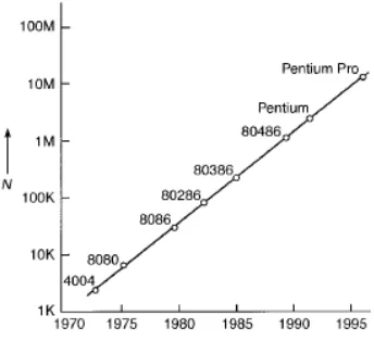
Figure 1.1. Original graph depicting Moore’s law, forecasting the advancement of
Figure 1.12. STM images area shown of an octadecanethiol SAM on gold. (a) Initial 400 x 400 nm image. (b) Image of the same area after scanning a 100 x 100 nm box four times. The patterned area is visible in the center of the image. Scanning conditions were held constant at a bias of 300 mV, a set point of 0.1 nA, and a scan rate of 1.34 Hz.42 ... 22 Figure 1.13. STM images (300 x 300 nm) of octadecanethiol SAMs after patterning a
roughly 50 x 50 nm feature. (a) Image after scanning a 50 x 50 nm area at lower biases and 75% relative humidity (RH), which shows no discernable difference in the topography. (b) Image after scanning a 50 x 50 nm area at 3 V and 6.6% RH. (c) Image after scanning a 50 x 50 nm area at 3 V and 75% RH, showing a depression of 0.29 nm in depth. All images were captured with a grey scale of 2 nm, a bias of 0.3 V and a set point current of 150 pA.43 ... 23 Figure 1.14. STM images (1 µm and 1 µm) of alkanethiols on gold illustrating patterns of the letters “NCSU” in which (A) dodecanethiol replaced a decanethiolate SAM (Vwrite=+3.8 V; Vread=+1 V; I=6.0 pA; ca. 60% RH) and (B) decanethiol replaced dodecanethiolate
(Vwrite=+3.6 V; Vread=+1.0 V; I=8.0 pA; ca. 60% RH).39 ... 24 Figure 1.15. STM images of FcC11S-SAM mesoscale chemical gradients fabricated in a dodecanethiol SAM by systematically varying replacement bias (A), or lithographic scan rate (B), while maintaining all other STM parameters constant. Replacement condition limits are annotated in images. The averaged section analysis is shown to the right of each gradient structure. All images were captured after the gradients were formed with a z-scale of 5 nm, bias of 1 V, set point current of 8-10 pA, and scan rate of 1 Hz.38 ... 27 Figure 1.16. Series of STM images of a range of different alkanethiol SAMs on gold where replacement lithography was attempted at incrementally higher biases. The designation – SCn denotes the chain length of the initial SAM. A series of lines of 100 nm in length were written with the biases indicated above and relative humidity held constant at 55%±2%. Imaging conditions: z-scale=3 nm; Bias=1.5 V; set point current=10 pA; and scan rate=1.0 Hz.41 ... 28 Figure 2.1. STM image (400 x 400 nm) of a decanethiol vapor deposited SAM on the
Figure 2.5. STM image of an annealed dodecanethiol SAM on gold showing mesoscale lines. SAM was fabricated by heating a gold substrate in a 1 mM solution of the alkanethiol in ethanol. Then, this sample was annealed in an oil bath at 110°C for four hours. Image was captured at a bias of 1 V, set point of 10 pA, and a scan size of 250 x 250 nm. The more narrow, parallel lines in the image running diagonally are artifacts from the STM and are not real surface features. ... 44 Figure 2.6. Diagram illustrating a convincing explanation regarding the appearance of stripes when annealing alkanethiol SAMs on gold. ... 45 Figure 2.7. STM image of a dodecanethiol SAM made by immersing a gold bead in neat dodecanethiol (a) heated for 1 h at temperatures exceeding 100°C and (b) maintained at room temperature for 24 h. ... 48 Figure 2.8. STM images of dodecanethiol SAMs fabricated by refluxing gold bead
substrates in (a) 1 mM and (b) 0.01 mM concentrations of the adsorbent in ethanol. After formation of both dodecanethiol SAMs, sample were immersed in a 1 mM solution of dodecanethiol in ethanol at room temperature. Images were captured at a bias of 1 V, a set point of 10 pA, and a z-range of 3 nm. ... 49 Figure 2.9. STM image of lines composed of FcC11SAc written into a dodecanethiol SAM made from 0.01 mM solutions of the adsorbent in ethanol. The image was captured at a bias of 1.5 V and 10 pA. ... 49 Figure 2.10. Graph of percent replacement versus bias used to make the replacement
lithography lines composed FcC11SAc. Percent replacement is shown at biases 2.6 V to 3.3 V. ... 51 Figure 2.11. STM image of a decanethiol SAM on a gold bead made from vapor deposition at 100°C for 12 h in a PFA vial. ... 53 Figure 2.12. STM image (250 x 250 nm) of decanethiol SAM made from vapor deposition at 100°C for 18 days in a PFA vial ... 54 Figure 3.1. Proposed reaction for the etching of GaAs with HCl.1 ... 63 Figure 3.2. Consecutive STM images of the same scan area of a dodecanethiol SAM on GaAs (a) Initial scan of the area. (b) Image of this same area after the completion of the first scan. The z range is set at 10 nm where greater heights are shown as lighter areas and smaller heights are shown as darker areas of the image. Images were scanned with a bias of 1 V and set point current of 150 pA. ... 64 Figure 3.3. STM image of a dodecanethiol SAM on GaAs scanned under a scanning bias of -1 V and set point current of 30 pA with the sample area purged with nitrogen. ... 66 Figure 3.4. STM image of (a) bare GaAs that was etched with 80% concentrated HCl/EtOH for 1 min and (b) dodecanethiol SAMs on GaAs where etching was done under the same conditions as in (a) then the GaAs was immersed in 1 mM dodecanethiol in ethanol for 24 h to make the SAM. Scanning conditions of 20 pA and -1 V were used to capture these
images. ... 67 Figure 3.5. STM images of a dodecanethiol SAMs on GaAs (a) before and (b) after
than 20 h. Replacement lithography was attempted with FcC11SAc in dodecane as the replacing solution where 9 lines were written at incrementally higher biases ranging from 2.5 to 3.3 V... 71 Figure 3.6. STM images of (a) bare GaAs that was etched in NH4OH for 45 seconds and (b) a dodecanethiol SAM on GaAs made by first etching in NH4OH, then immersing the sample in a solution of a mixture of NH4OH and dodecanethiol in ethanol. The image was captured at a bias of -1 V and set point of 10 pA. ... 72 Figure 3.7. STM image of a dodecanethiol SAM on GaAs scanned at 10 pA and -1 V where the box pattern in the middle of the image was formed previously by scanning under the same conditions, except at a scan size of 500 x 500 nm (half the scan size). The sample was prepared using NH4OH to etch the GaAs and during deposition of the SAM. ... 74 Figure 4.1. A series of STM images comparing the process of adventitious replacement of FcC11SAc into a C10≡ SAM (top, panels A, C, and E) and a C12SH SAM (bottom, panels B, D, and F). Images were taken before FcC11SAc was added (A, B), 20 min (C, D), and 60 min after addition of FcC11SAc (E,F). ... 82 Figure 4.2. Schematic showing process used to quantify the amount of adventitious
replacement for each STM image collected: (A) raw image; (B) fit to a sum of two
Gaussians. ... 83 Figure 4.3. Comparison of adventitious replacement with 50 µM of FcC11SAc into C10≡
(black squares) and C12SH (red circles) SAMs. Error bars are 90% confidence intervals derived from multiple trials. ... 84 Figure 4.4. Comparison of adventitious replacement with 10 µM of FcC11SH into C10≡
(black squares) and C12SH (red circles) SAMs with error bars at each point representing 90% confidence intervals derived from multiple trials. ... 85 Figure 4.5. Graph showing time dependence of the average fractional surface coverage of FcC11SAc as it replaced into a C10≡ SAM by 5 µM (blue stars), 25 µM (orange triangles), 50 µM (black squares), and 100 µM (red circles) concentrations of the replacing molecule with error bars at each point representing 90% confidence intervals derived from multiple trials. The red lines are a best fit of a first-order Langmuir equation to the points. Note that the values in Table 4.1 are the average of fits of individual trials where these are fits of the average values of all the trials. ... 86 Figure 4.6. Graph showing the average adventitious replacement as fractional surface
Figure 5.2. A representative STM image showing a set of lines written with replacement lithography where Fc-C≡C-p-C6H4-C≡C (Ink 2) was replaced into a C12SH SAM. A set of
nine lines were written at increasing biases (from left to right). ... 105 Figure 5.3. Comparison of percent replacement in lines written by replacement lithography on a C12SH SAM at varying biases. Red points designate replacement with Ink 1
(thioacetate), and black points designate replacement with Ink 2 (terminal alkyne). Error bars indicate 90% confidence intervals from the average values obtained from multiple trials. ... 106 Figure 5.4. (A) STM image (55 x 55 nm) of a mixed SAM of dodecanethiol and
dodecaneselenol on gold prepared from a 4:1 solution of the selenol to the thiol. Inset is a 20 x 20 nm image. The blue circle highlights an area of dodecanethiolate, which is of a higher apparent height compared to the surrounding dodecaneselenol. All images were collected at -1 V and 1.0 pA tunneling current. (B) Scan profile drawn through an area composed of both molecules showing the difference in apparent height between these two SAM forming molecules.7 ... 108 Figure 5.5. A representative STM image of a set of lines written with replacement
lithography where Fc-C≡C-p-C6H4-C≡C (Ink 2) was replaced into a C12SH SAM. A set of seven lines were written at a bias of 3.2 V (from left to right). These lines were captured at a bias of 2 V, although other images were taken of these lines at other biases. ... 109 Figure 5.6. Graph showing height contrast versus bias used to capture lines composed of Ink 1 (red circles) and Ink 2 (black squares) made from replacement lithography. Error bars indicate 90% confidence intervals from the average values obtained from multiple trials. . 110 Figure 6.1. A series of STM images comparing the process of adventitious replacement of FcC11SH into a C12SH SAM (top, panels A, C, and E) and a C12NC SAM (bottom, panels B, D, and F) on Platinum. Images were taken before FcC11SH was added (A, B), 5 min (C, D), and 60 min after addition of FcC11SH (E,F). ... 119 Figure 6.2. Comparison of adventitious replacement with 0.5 µM of FcC11SH into C12NC (black squares) and C12SH (red circles) SAMs. Error bars are 90% confidence intervals derived from multiple trials. ... 121 Figure 6.3. Graph showing the average adventitious replacement as fractional surface
Chapter 1 - INTRODUCTION
1.1 Miniaturization of Electronics
As predicted by Gordon E. Moore in the mid 1960s there has been a continued demand to push electronic components to smaller dimensions to allow for increased functionality within a restricted amount of space.1 Moore predicted that the number of transitors in a circuit will double every 18 months. Figure 1.1 shows the original graph forecasting this trend. As shown in Figure 1.2, which is an updated version of this graph, this prediction has held true up until the present.2 Along with integrated circuits, there is a
demand to fabricate nanostructures for a variety of applications.
It is generally accepted that photolithography, the main tool responsible for allowing the trend shown in Figure 1.1 to hold true, will have to be replaced by another technique for patterning surfaces due to various limitations.2-5 In photolithography, complex patterns are made to form the intricate network of transistors necessary to form an integrated circuit.2,5 A crucial step in forming this network of transistors involves directing light through a mask, which is patterned beforehand, to allow for one to project a desired pattern onto a
Figure 1.1. Original graph depicting Moore’s law, forecasting the advancement of microprocessor
miniaturization.1
Figure 1.2. Graph showing how the advancement of microprocessor manufacturing has continued to
follow Moore’s law into the present from 1973. N=number of transitors/chip.2
surfaces can be defined as a method for creating patterns where one starts from a larger pattern and progressively decreases the dimensions of the pattern until features reach the desired size. Alternately, a “bottom-up” approach for patterning is a technique where one starts with small amounts of material and progressively adds more of the material in a controlled, confined manner. However, both “bottom-up” and “top-down” methods for patterning surfaces have been shown to have limitations.5 Many “bottom-up” approaches have yielded nanostructures with dimensions smaller than 10 nm with relative ease compared to most “top-down” approaches, which have pushed down to the nanometer length scale, but have become quite elaborate and expensive.2,5 So, it has been proposed that a “bottom-up” approach, using self-assembly, could be used as a means to organize molecules so they can function as a device.3 For instance, there has been extensive interest in using molecules with interesting electronic properties to act as various components in a nanoscale device,
especially in integrated circuits.3,4,7 However, despite the relative ease at which one can make nanometer scale structures through some “bottom-up” approaches, making elaborate patterns using these methods and incorporating these methods to build structures for various applications has proven to be difficult.5
nanodots of 4-8 nm in diameter onto the nanoelectrodes.8 It was suggested that this method could possibly be used to make silicon nanodot based transistors, providing more control could be established during silicon nanodot assembly. It is clear that the best approach for fabricating devices at the nanoscale will depend on the type of device desired and the function, so investigating new methods for patterning and controlling functionality across surfaces is highly desirable for the advancement of various technologies.2
1.2 Scannning Probe Microscopy
Scanning probe microscopy (SPM) is a group of techniques that allows for one to image and manipulate matter at the nanoscale.9,10 In general, when imaging the morphology of a surface using SPM, the interaction (ideally a non-destructive interaction) of a sharp probe with the surface is being measured. The probe is raster scanned across the surface while being in close proximity to it. The probe is close enough to where the interaction with the surface is on the order of a few nanometers or less.
Atomic force microscopy (AFM) is one type of SPM technique where the morphology of a surface is measured by monitoring the attractive and repulsive forces
between a probe and surface as the probe is being scanning across the surface.10,11 The probe being used in AFM is actually a sharp tip on the end of a cantilever. If the sharp tip is
is used to modulate this interaction and keep the tip within close proximity to the surface during scanning. This feedback system applies a voltage to drive a piezo that controls the z−axis movement of the tip (e.g. height of the tip) relative to the surface. Another set of piezos drives the raster scanning process across the surface and defines the area to be
scanned. The overall deflection of the tip and controlled raster scanning of the surface allows one to measure the morphology of the surface. This type of tip repulsion and attraction exist universally for all materials, so most types of samples can be imaged with AFM.10
Therefore, one can obtain very accurate height contrast data (the height difference between different points on a surface) regardless of the composition of the surface.11
Scanning tunneling microscopy (STM) is a related SPM technique where imaging is accomplished through monitoring the tunneling current between the tip and sample.10-13 First demonstrated by Binning and Rohrer in 1982, STM is very similar to AFM in that
topography is measured by raster scanning a tip over a surface while monitoring an
height is adjusted through the help of a feedback mechanism to keep this current constant. In height mode the tip absolute height remains constant and the change in tunneling current is recorded as the tip encounters height changes across the surface (Figure 1.3). This tunneling current change can be translated to a height change. In either mode it can be said that “what is converted into an image in STM is either the spatial variation of the tunneling current or the spatial variation of the tip height.”10
Figure 1.3. Diagram of STM operation (not drawn to scale). PX and PY are piezo elements that scan the
tip along the x- and y-axis. In constant current mode, VP is the voltage applied to PZ piezo element (peizo
that controls z-axis movement), which adjusts tip height while VT (tunneling voltage) and JT (tunneling
current are held constant.13
Imaging by STM is dependent on electronic tunneling, a quantum mechanical phenomenon, and a relatively simple quantum mechanical equation can be applied here.14 Classical theory describes electrons as finite particles where tunneling is forbidden, which fails to explain electronic tunneling in STM. However, in quantum theory, electrons behave
occur from the overlap of the wave functions of two mechanically and electronically separated electrodes upon the application of a bias (Figure 1.4). The equation below
(Equation 1.1) is a simplified quantum mechanical treatment describing electronic tunneling through a planar barrier.13 In this equation ψ is defined as the tunneling barrier height
(related to work function), S is the tunneling barrier width, JT is the tunneling current, and A=1.025A-1eV-1/2).
JTαe−Aψ1/ 2S;A=(4 / )2π h m1/ 21.1
Further analysis of Equation 1.1 shows that barrier height (ψ ) affects the tunneling
current, which implies that changes in barrier height (or type of material on the surface) can affect the tunneling current and cause inaccurate height contrast data.13 Barrier height is related to the work function of a material. If the composition of the surface is uniform, than the work function is uniform and accurate height contrast data can be collected. However, when the surface composition is not uniform, then the work function changes. Since
tunneling current is also exponentially dependent on barrier height (as well as barrier width), small changes in the work function should cause large changes in the tunneling current, which will make collecting accurate height contrast data difficult. Surface topography can still be collected, but one has to keep in mind that the apparent height contrast data will reflect both changes in physical height and work function.10 Since few surfaces are perfectly uniform in composition and structure, STM height data is more accurately described as apparent height contrast data.
Since being invented, SPM techniques, especially STM and AFM, have allowed one to manipulate and study the properties of a variety of surfaces at the nanoscale.9,10 Part of what makes various STM and AFM techniques capable of resolving and manipulating structures at the atomic scale is their high resolution. Both STM and AFM achieve these tasks through sharp probes that interact with the surface via some sort of mechanism. Since, in these techniques the mechanism varies, this allows for a variety of methods to induce local surface modification at nanometer length scales.9,10
1.3 Alkanethiol Self-assembled Monolayers on Gold
The formation and structure of alkanethiol SAMs on gold have been widely studied.2 However, there are many details about the binding and formation of these films that are still highly debated.7
Figure 1.5. One proposed reaction for alkanethiol adsorption onto gold. Various studies have suggested that evolution of hydrogen gas occurs in vacuum deposition of alkanethiol, but the fate of the hydrogen
during solution deposition is still highly debated.7,16-18
It has generally been accepted that alkanethiols bind to gold as alkanethiolates (RS-) where sulfur binds to the surface and the hydrogen is lost.17 The bond that forms between the gold and sulfur is strong enough to persist in ambient conditions, but evidence has been found that under conditions of elevated temperature the thiolates covert to disulfides and desorb from the surface.7 At some point during adsorption of thiols onto gold, the hydrogen is lost, but the mechanism for this process and fate of the hydrogen has not been
unambiguously determined.2,7 In one proposed mechanism, it was proposed that when the monolayer is vapor deposited in vacuum, the hydrogen is lost as H2 gas (Figure 1.5).7 Alternately, it has been suggested that when the monolayer is formed in solution in ambient conditions, oxygen assists in oxidative conversion of hydrogen to water.
In general, more is known about the final structure of alkanethiol SAMs. When fully formed on gold, these films adopt an ordered structure described by (√3 × √3)R30 unit cell.7,16-18 Each of the sulfur groups tend to bind to a three-fold hollow site, but some studies have suggested that binding can occur over a bridge site (in between two gold atoms).7 Figure 1.6 shows a representation of the (√3 × √3)R30 structure of alkanethiols on gold with the yellow circles indicating the sulfur binding position to the gold atoms (white circles) at the three-fold hollow site. These alkanethiol molecules tilt 30° from the surface normal to maximize van der Waals interactions between the alkyl chains (Figure 1.7).7,16,18,24
Figure 1.6. Illustration showing the arrangement of sulfur atoms in the alkanethiols adsorbed onto gold. The sulfur atoms (yellow circles) adsorb across a three-fold hollow site. The distance between each
neighboring sulfur atom (indicated by red lines connecting the six yellow circles) make up the (√3 ×
√3)R30 unit cell. There is a 30° difference in alignment of this unit cell and the order of the gold atoms.
However, it has been strongly suggested that alkanethiol SAMs on gold have more complicated ordering.7,24 For instance, recently it has been argued that alkanethiol SAMs on gold preferentially form a orthorhombic c(4 × 2) secondary superlattice structure, but the exact structure of this phase has been debated.7,16,18,24-26 It is suggested that the (√3 ×
√3)R30 unit cell can be used to describe the position of the sulfur groups, but the orientation of the alkanethiol chains are different.7,16,18,24-26 The c(4 × 2) phase can also be described as a 2√3a × 3a unit cell (where a equals the gold lattice constant). The differing chain
Figure 1.8. Diagram showing a proposed c(4 × 2) superlattice structure of an alkanethiol SAM on gold where wedges indicate the tilt direction of the chains and dark circles indicate the sulfur atoms. The
smaller dashes show the c(4 × 2) structure and the large dashes show the equivalent 2√3a × 3a unit cell
where a equals the gold lattice constant.7
however, it has been found that the type of solvent and many other conditions have an effect on the final structure.7 For example, when employing STM to probe the effect of the
underlying substrate flatness on structure of the resulting SAM, it was discovered that rough surfaces yield SAMs with multiple phases, but flatter surfaces tend to yield monolayers with only the c(4 × 2) phase.30 The effects of some of other variables on defects will be
elaborated on later in this document.
occurs near 70 °C. In general, however, alkanethiolate SAMs on gold have a relatively high degree of order and, with the caveats expressed above, are reasonably stable.
1.4 Scanning Probe Lithography
Various SPM techniques have been employed to create nanostructures on surfaces coated with SAMs.12,15,32 As mentioned previously, SPM techniques utilize probes that extend down to the nanometer scale, providing a means to measure topography and
manipulate the surface at this length scale. This type of lithography is called scanning probe lithography (SPL) and most often initiates the creation of patterns on surfaces via a
mechanical interaction, electrochemical reaction, or through high electric fields. In addition to SAMs being a useful way to change the functionality across a surface, these films are amenable to having their functionality changed locally through the use of SPL.15 Through the use of this type of lithography, patterns can be formed on surfaces where one can vary the tail group of the molecules being added or removed to locally control the functionality of the surface. The use of both self-assembly to make the monolayers and SPL to locally modify the film can be considered a combination of both bottom-up and top-down approaches for patterning surfaces.
diffusion of the ink onto the substrate. Initially, this group focused on illustrating DPN with octadecanethiol (C18SH) on gold (Figure 1.9).
Figure 1.9. (A) Lateral force microscopy (LFM) image of a 1 x 1 µm area square composed of
octadecanethiol (C18SH ) on gold written by DPN. (B) LFM image of a 3 µm long vertical line composed
of C18SH written by DPN, which is 30 nm in width. (C) LFM image of a line composed of C18SH written by DPN on gold, which is 100 nm in width. Darker areas in the LFM images above correspond to areas
of relatively lower friction.33
The versatility of DPN has been demonstrated by extending this SPL technique to other systems, such as different substrates.33,34 For example, DPN has been extended to use on oxidized GaAs and silicon with hexamethyldisilazane (HMDS) as the ink where patterns with 100 nm dimensions were made. The silazane end unit in the HMDS reacted
preferentially with the oxide surface forming trimethylsilyl group on the surface and
pattern the surface simultaneously. Employing one feedback loop to control the array of tips allowed this technique to remain relatively simple. Since one feedback system was used, the force applied by each cantilever varied significantly. However, similar line widths and quality lines were created despite the differences in force applied by the cantilevers.
STM offers an alternate SPL method for patterning surfaces that relies on different interactions with the surface to initiate patterning compared to SPL patterning techniques that rely on AFM.15,32,36-44 STM has often been applied to pattern alkanethiol SAMs on gold, but many other surfaces have been patterned as well with this technique.
Figure 1.10. STM images (100 x 100 nm) of an octadecanethiol SAM on gold. (a) Image taken at 1 V and 1 nA where no significant change occurs in the surface. (b) Image of the same area after scanning at 10 x 10 nm area at lower bias of 10 mV and higher tunneling current of 10 nA. The 10 x 10 nm area is within
the region outlined by the broken line, which shows the presence of pits.40
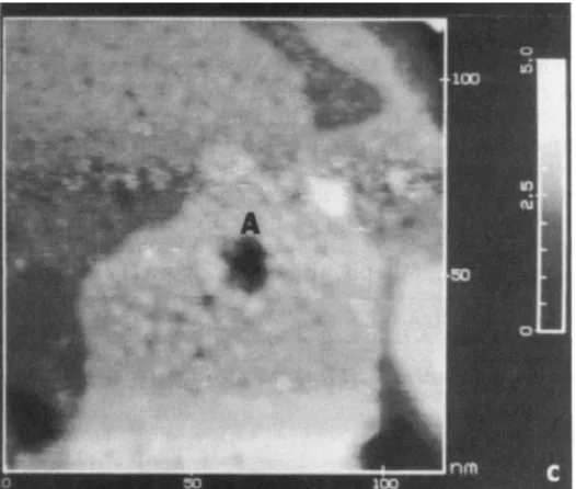
depressions were observed that were similar to ones made under mechanical desorption. Figure 1.11 shows a depression made while exposing a confined area to 3 V (labeled A). When elevating the bias, the STM current becomes less a tunneling current and more a field emission current. It was argued that his behavior allows for molecules to be ionized and ejected from the surface. Consequently, a field ionization mechanism was proposed, but it is difficult to rule out any other mechanism for desorption because no evidence was shown to support these claims.
Figure 1.11. STM image (120 x 120 nm) of a n-octadecanethiol SAMon gold after applying a 3 V bias and 1 nA pulse. The pulse caused the formation of a pit, which indicated as A. All images were capture at
V = 1 V and It (set point current) = 1 nA.40
First, depressions were formed in the C18SH SAM under conditions of relatively low bias and high current similar to what was employed by Kim and Bard above.42,43 Under these scanning conditions of 300 mV and 0.1 nA, depressions were formed in the surface with debris present along the outside of the patterned areas (Figure 1.12a and b).42 It was observed that additional scanning over the patterned area tended to remove the debris. Additional observations were made that supported a mechanical desorption mechanism. For instance, the apparent height contrast between the removed monolayer area and the
Figure 1.12. STM images area shown of an octadecanethiol SAM on gold. (a) Initial 400 x 400 nm image. (b) Image of the same area after scanning a 100 x 100 nm box four times. The patterned area is visible in the center of the image. Scanning conditions were held constant at a bias of 300 mV, a set point of 0.1 nA,
and a scan rate of 1.34 Hz.42
the tip away from the surface, it was concluded that an electrochemical mechanism, strongly influenced by the presence of water was responsible for the desorption behaviors observed.
Figure 1.13. STM images (300 x 300 nm) of octadecanethiol SAMs after patterning a roughly 50 x 50 nm feature. (a) Image after scanning a 50 x 50 nm area at lower biases and 75% relative humidity (RH), which shows no discernable difference in the topography. (b) Image after scanning a 50 x 50 nm area at 3 V and 6.6% RH. (c) Image after scanning a 50 x 50 nm area at 3 V and 75% RH, showing a depression of 0.29 nm in depth. All images were captured with a grey scale of 2 nm, a bias of 0.3 V and a set point
current of 150 pA.43
Figure 1.14. STM images (1 µm and 1 µm) of alkanethiols on gold illustrating patterns of the letters
“NCSU” in which (A) dodecanethiol replaced a decanethiolate SAM (Vwrite=+3.8 V; Vread=+1 V; I=6.0 pA;
ca. 60% RH) and (B) decanethiol replaced dodecanethiolate (Vwrite=+3.6 V; Vread=+1.0 V; I=8.0 pA; ca.
60% RH).39
compared to the background SAM. An area of lower apparent height results due to the decreased tunneling probability associated with this region of greater film thickness. In another case, a 3.6 V bias was used to remove regions of a dodecanethiol SAM, which allowed decanethiol ink molecules to fill these vacated areas. Figure 1.14b is a STM image showing this replacement where an ink of shorter chain length was replaced into a SAM composed of molecules with a longer chain length. The patterned regions appear as areas that are brighter and of higher apparent height because of the increased tunneling probability associated with this region of smaller thickness. When scanning these same lines in air (after removal of the ink solution), a reversal of the height contrast was observed where the
patterned area had a shorter apparent height compared to the background SAM. This observation helped confirm the contents of these patterned areas.
(FcC11SAc), which offered a means to construct nanopatterns with interesting electronic properties and limit unwanted spontaneous replacement.38,41 When employing FcC11SAc as the ink molecule, the replaced areas had an increased apparent height compared to the
background because of the greater conductivity of regions composed of this ink. This higher apparent height of the replaced regions provided better distinction between the background SAM and patterned areas. Also, it was shown that this ink molecule with a thioacetate head group could be used in replacement lithography in place of a alkanethiol and it displayed less spontaneous, unwanted replacement. It was speculated that some of the thioacetate could deprotect in situ to form a thiolate, which can then bind to gold, but a significant amount of
the ink molecule remained as the thioacetate and this limited the amount of adventitious replacement. A more recent study by Lee et al. showed that alkanethiocetates form SAMs on gold, but at a relatively slower rate compared to the corresponding alkanethiol.47 It was suggested, especially through X-ray photoelectron spectroscopy (XPS), that the binding species is still the thiolate, but that the thioacetate protecting group hindered the formation of this species.
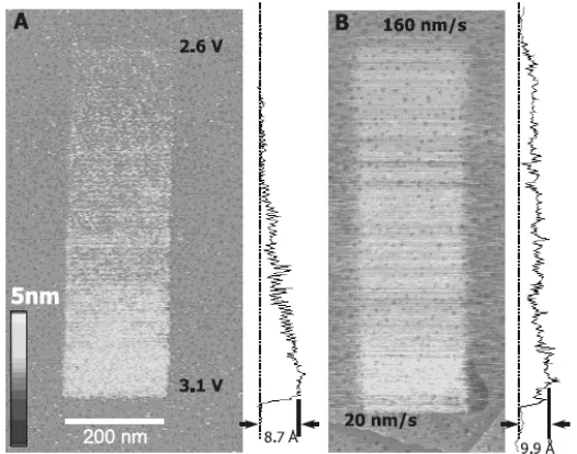
In one report, the effect of scanning parameters, such as scan rate and writing bias on the replacement during replacement lithography was explored qualitatively by making gradients with FcC11SAc as the ink.38 These gradients were made by incrementally decreasing or increasing these variables while scanning across a given area of a
was observed. It was shown that as lithographic scan rate was increased, the amount of replacement decreased (Figure 1.15). In contrast, if bias was incrementally increased, the amount of replacement increased.
Figure 1.15. STM images of FcC11S-SAM mesoscale chemical gradients fabricated in a dodecanethiol
SAM by systematically varying replacement bias (A), or lithographic scan rate (B), while maintaining all other STM parameters constant. Replacement condition limits are annotated in images. The averaged section analysis is shown to the right of each gradient structure. All images were captured after the gradients were formed with a z-scale of 5 nm, bias of 1 V, set point current of 8-10 pA, and scan rate of
1 Hz.38
In later reports, this same FcC11SAc ink was used to probe the effect of the SAM-substrate composition on the amount of replacement provided by replacement
Figure 1.16. Series of STM images of a range of different alkanethiol SAMs on gold where replacement lithography was attempted at incrementally higher biases. The designation –SCn denotes the chain length of the initial SAM. A series of lines of 100 nm in length were written with the biases indicated above and relative humidity held constant at 55%±2%. Imaging conditions: z-scale=3 nm; Bias=1.5 V;
set point current=10 pA; and scan rate=1.0 Hz.41
found to have less order by STM. As a consequence, the authors argued that SAMs with more order in their structure were less prone to being replaced.
In another report, Gorman et al. probed the effect of substrate on the amount of replacement.44 As before, a series of lines were written in a SAM at incrementally higher biases and the amount of replacement was compared between different assemblies. Here, the amount of replacement was compared between dodecanethiol SAMs on gold, palladium, and platinum. Replacement of these SAMs on gold occurred at lower biases then on palladium or platinum.
There are some limitations using replacement lithography to pattern surfaces. As a means to pattern surfaces, replacement lithography is like most “writing techniques” because each feature has to be written independently, so this process is serial and relatively slow. Despite efforts to make SPL techniques into a more parallel technique, it has been shown that it will be difficult for any of these techniques to rival the output of photolithography for making patterns. As a consequence, it is unlikely that replacement lithography will be suitable for applications where high throughput is necessary.
1.5 References
(1) Moore, G. E. Proc. IEEE1998, 86, 82-85.
(2) Xia, Y.; Whitesides, G. M. Angew. Chem.1998, 37, 550-575.
(3) Balzani, V. ChemPhysChem2003, 4, 49-59.
(4) Tour, J. M. J. Am. Chem. Soc.1998, 120, 8486-8493.
(5) Whitesides, G. M.; Love, J. C. Sci. Am.2001, 285, 38-48.
(6) Lehn, J.-M. Proc. Natl. Acad. Sci. U. S. A.2002, 99, 4763-4768.
(7) Love, J. C.; Estroff, L. A.; Kriebel, J. K.; Nuzzo, R. G.; Whitesides, G. M. Chem. Rev. (Washington, DC, U. S.)2005, 105, 1103-1169.
(8) Mizuta, H.; Oda, S. Microelectronics Journal2008, 39, 171-176.
(9) Bottomley, L. A. Anal. Chem.1998, 70, 425-476.
(10) Magonov, S.; Whangbo, M.-H. Surface Analysis with STM and AFM; VCH
Verlagsgesellschaft mbH and VCH Publishers, Inc: Weinheim (Federal Republic of Germany), 1996.
(11) Binnig, G.; Quate, C. F.; Gerber, C. Phys. Rev. Lett.1986, 56, 930-933.
(12) Baski, A. A. Advanced Semiconductor and Organic nano-techniques, Part 32002,
1-20.
(13) Binning, G.; Rohrer, H.; Gerber, C.; Weibel, E. Phys. Rev. Lett.1982, 49, 57-61.
(14) Wassel, D. Dissertation, North Carolina State University, 2004.
(19) Guo, Q.; Sun, X.; Palmer, R. E. Phys. Rev. B: Condens. Matter2005, 71, 1-5.
(20) Schreiber, F. Prog. Surf. Sci., 65, 151-257.
(21) Ulman, A. Chem. Rev. (Washington, DC, U. S.)1996, 96, 1533-1554.
(22) Vericat, C.; Vela, M. E.; Salvarezza, R. C. Phys. Chem. Chem. Phys.2005, 7,
3258-3268.
(23) Bain, C. D.; Whitesides, G. M.; Troughton, E. B.; Tao, Y.-T.; Evall, J.; Nuzzo, R. G.
J. Am. Chem. Soc.1989, 111, 321-335.
(24) Poirier, G. E.; Tarlov, M. J. Langmuir1994, 10, 2853-2856.
(25) Poirier, G. E. Langmuir1997, 13, 2019-2026.
(26) Touzov, I.; Gorman, C. B. J. Phys. Chem. B1997, 101, 5263-5276.
(27) Kautz, N. A.; Kandel, S. A. J. Am. Chem. Soc.2008, 130, 6908-6909.
(28) Porter, M. D.; Bright, T. B.; Allara, D. L.; Chidsey, C. E. D. J. Am. Chem. Soc.1987, 109, 3559-3568.
(29) Biebuyck, H. A.; Bain, C. D.; Whitesides, G. M. Langmuir1994, 10, 1825-1831.
(30) Godin, M.; Williams, P. J.; Tabard-Cossa, V.; Laroche, O.; Beaulieu, L. Y.; Lennox, R. B.; Grütter, P. Langmuir2004, 20, 7090-7096.
(31) Bumm, L. A.; Arnold, J. J.; Charles, L. F.; Dunbar, T. D.; Allara, D. L.; Weiss, P. S.
J. Am. Chem. Soc.1999, 121, 8017-8021.
(32) Garcia, R. R.; Martinez, R. V. R. V.; Martinez, J. J. Chem. Soc. Rev.2006, 35, 29-38.
(33) Piner, R. D.; Zhu, J.; Xu, F.; Hong, S. H.; Mirkin, C. A. Science1999, 283, 661-663.
(34) Ivanisevic, A.; Mirkin, C. A. J. Am. Chem. Soc.2001, 123, 7887 -7889.
(35) Hong, S. H.; Mirkin, C. A. Science2000, 288, 1808-1811.
(36) Abeln, G. C.; Hersam, M. C.; Thompson, D. S.; Hwang, S. T.; Choi, T.; Moore, J. S.; Lyding, J. W. J. Vac. Sci. Technol., B1998, 16, 3874-3878.
(38) Fuierer, R. R.; Carroll, R. L.; Feldheim, D. L.; Gorman, C. B. Adv. Mater. (Weinheim, Ger.)2002, 14, 154-157.
(39) Gorman, C. B.; Carroll, R. L.; He, Y. F.; Tian, F.; Fuierer, R. Langmuir2000, 16,
6312-6316.
(40) Kim, Y. T.; Bard, A. J. Langmuir1992, 8, 1096-1102.
(41) Lewis, M. S.; Gorman, C. B. J. Phys. Chem. B2004, 108, 8581-8583.
(42) Ross, C. B.; Sun, L.; Crooks, R. M. Langmuir1993, 9, 632-636.
(43) Schoer, J. K.; Zamborini, F. P.; Crooks, R. M. J. Phys. Chem.1996, 100,
11086-11091.
(44) Williams, J.; Gorman, C. B. Langmuir2007, 23, 3103-3105.
(45) Bucher, J. P.; Santesson, L.; Kern, K. Langmuir1994, 10, 979-983.
(46) McCarley, R. L.; Dunaway, D. J.; Willicut, R. J. Langmuir1993, 9, 2775-2777.
(47) Béthencourt, M. I.; Srisombat, L.-o.; Chinwangso, P.; Lee, T. R. Langmuir2009, 25,
Chapter 2 - EFFECT OF DEFECTS ON REPLACEMENT LITHOGRAPHY
2.1 Introduction: Types of Defects in Alkanethiol SAMs on Gold
As described earlier, alkanethiol molecules exposed to a gold surface spontaneously form SAMs with a high degree of order. Despite their high degree of order, many defects in these films exist that can affect their properties.1 One example where defects can be
important is when SAMs are employed as electrochemical blocking layers. Here, the presence of defective sites in the film can provide a pathway for species to come into close proximity with the surface where they can be oxidized or reduced.2
density and order. Domain boundaries typically link pits together, which are defects that are present as circular depressions in a SAM.
There has been a great deal of interest in pits, especially in defining the structure of these features, but a number of studies have concurred that these defects are due to
depressions in the underlying gold.6-10 It has been debated whether pits are defects caused by missing alkanethiol molecules (pin holes) or removed gold atoms, equal in depth to the height change of monoatomic steps. One group explored these defects in hexanethiol (C6SH) and docosanethiol (C22SH) SAMs with STM.7 These molecules have drastically different lengths, so SAMs composed of these molecules should have significantly different
thicknesses. If the pits in SAMs made from these two molecules are due to missing alkanethiol molecules, the depths of the pits should be significantly different and should correspond roughly to the known thickness of the SAMs. When imaging the C22SH SAM on gold, the authors identified regions that had measured depths of roughly 25 Å, which
these depths tended to correspond closely with the diameter of a gold atom.6-10 As with many other studies, Schӧnenberger et al used STM to confirm these results.10 In addition, these authors used STM to preferentially image either the gold or SAM lattice by changing the resistance (or bias) during scanning. When preferentially imaging the gold surface, depressions could be seen in the surface. More significantly, when imaging the SAM, the authors were able to resolve the SAM structure within the pits, which suggest that these depressions contain alkanethiol molecules and are not equivalent to pin hole defects. Others have been able to resolve the SAM structure within these pits and have confirmed this result.6 As a result, it has been generally accepted that the pits contain alkanethiol molecules and are depression in the gold, but this still raises questions about how this defect and others form.
The formation of defects in alkanethiol SAMs on gold are caused by both external and internal factors.1 Many of these defects seem to be influenced by conditions present during formation of these SAMs while other defects are present due to the complex intrinsic behavior of these molecules when adsorbed onto gold.
to affect pit density in particular. If pit density in alkanethiol SAMs can be reduced or completely removed, then, presumably, more ordered SAMs could be made.3
Since many processes are defect mediated, it became of interests to probe the effect of defect density and overall order on replacement lithography. STM allows one to
investigate defects and order in SAMs while also allowing one to perform replacement lithography. Experiments were performed where the defect density in dodecanethiol SAMs on gold was modulated by varying preparation conditions and the effect of the resulting structure on replacement lithography was explored.
2.2 Reducing Defects in SAMs by Vapor Deposition
2.2.1 Literature Precedent
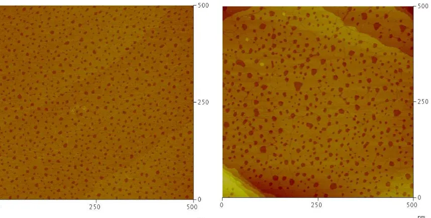
this SAM deposited on this same surface from solution yielded a significant number of pits. Also, if this vapor deposition procedure was applied to electrochemically polished gold or gold on the front side of mica, then high pit density was observed.
Figure 2.1. STM image (400 x 400 nm) of a decanethiol vapor deposited SAM on the backside of gold peeled from mica. Images were collected at a scan rate of 2.3 Hz, 1 V bias, and 1 pA tunneling current.
Inset in the bottom right shows a 10 x 10 nm molecular scale image of the SAM.11
Although the above method formed SAMs having less pits compared to SAMs on annealed gold, it should be noted that Figure 2.1 shows that there was a higher density of step edges than what is observed when other procedures are followed.11 For instance, when forming alkanethiol SAM on annealed gold beads, large terraces composed of alkanethiol void of any step edges can be observed.3,13-15 In contrast, Figure 2.1 shows a SAM surface with a much greater density of step edges.11 As was discussed earlier, these step edge defects are very similar to pits as they are both defects in the gold surface that disrupt the order of the alkanethiol SAM by causing a height change equal to the diameter of a gold atom.
Consequently, it was of interest to apply this vapor deposition method for forming high alkanethiol SAMs with less pit density to an annealed gold bead or gold on mica surface, which has less step edge density. Thus, the above method developed by Touzov and Gorman was applied to more flat gold surfaces to determine if both pit density and step edge density could simultaneously be reduced by vapor deposition.
2.2.2 Results and Discussion
The procedure developed by Touzov and Gorman was followed but annealed gold beads or annealed gold on mica were used as the substrate in place of gold stripped from mica.11 This was done by annealing either a gold bead or gold on mica (see experimental section). These samples were placed in a ca. 100 mL glass jar with a lid modified to contain a septum. Then, deposition was performed via the method reported by Touzov and
Gorman.11
Figure 2.2. STM image of decanethiol vapor deposited SAM on gold on mica. The image was captured at a scanning bias of 1 V and set point of 10 pA.
As mentioned above, in the report by Touzov and Gorman it was claimed that the type of substrate was an important factor in creating pit free decanethiol SAMs.11 It is possible that this method can only be successful for creating pit free alkanethiol SAMs on a gold surface peeled from mica. However, this substrate is undesirable as the number of step edge defects in the SAM will be relatively high (Figure 2.1). In addition, in order to compare the effect of structure on replacement lithography according to previously described
methods,3,13-15 one has to measure percent replacement of lines drawn in the SAM.
literature describes other conditions that can modulate pit density, this attempt to follow the Touzov preparation closely was abandoned and other procedures for creating lower defect density alkanethiol SAMs were explored.
2.3 Reducing Defects in SAMs by Thermal Annealing in Air
2.3.1 Literature Precedent
Heating an alkanethiol SAM in air has been found to be another way to modulate defect density, especially pit density. Several reports utilize this treatment to remove pits in alkanethiol SAMs and show evidence that this treatment does not initiate the formation of other defects.6,8,16
imaged the resulting surface with STM. At elevated temperatures, between 72-75°C,
merging of pits occurred. Figure 2.3 is a reported STM image of a hexanethiol SAM on gold where a decrease in the density of pits was observed following this treatment. As with the previous study, it was claimed that pit density could be significantly reduced without creating other defects, but no molecular resolution STM images were presented to support this claim.
Figure 2.3. STM images of hexanethiol SAM on gold formed by immersing gold in 1 mM of the thiol in ethanol for 7 min. The resulting SAM was then heated to 345 K and this image was captured at 300 K.
The image was scanned at a bias of 50 mV, scan size 400 x 400 nm, and set point of 1 nA.16
In a third report, Cavalleri et al. showed that annealing SAMs could result in
decreased pit density.16 These authors heated a decanethiol SAM on gold from 77°C to 97°C while scanning the surface with STM. It was claimed that molecular scale STM images (not shown in the report) of these annealed SAMs showed “well-ordered alkanethiolate
2.3.2 Results and Discussion
A set of experiments were conducted to determine the veracity of the claims above. Alkanethiol SAMs were annealed under various conditions similar to what these authors employed. First, dodecanethiol SAMs were made from 1 mM ethanolic solution (see
experimental section), then annealed in air without much temperature control. STM images of these surfaces showed near complete removal of the pits (Figure 4a). It was discovered, however, that upon imaging the surface with molecule resolution, that the removal of the pits occurred in tandem with the appearance of molecular scale stripes (Figure 4b). Additional experiments confirmed that removing pits through excessive annealing of these alkanethiol SAMs lead to the appearance of these features across all areas of the SAM.
avoided. Dodecanethiol SAMs were made from a 1 mM ethanolic solution (see experimental section), then annealed in air at controlled temperatures (below 110°C). When temperatures below 100°C were employed, no significant changes in pit density were observed. When heating these dodecanethiol SAMs at temperatures between 100-110°C, the number of pits was reduced (Figure 2.5). However, in these images very thick lines could be seen at much larger scales than the molecular scale stripes observed above. Also, these lines were found randomly across the surface. Despite efforts to avoid the appearance of these features by modulating the annealing temperature, these structures were consistently seen whenever temperatures high enough to reduce pit density were used.
Figure 2.6. Diagram illustrating a convincing explanation regarding the appearance of stripes when annealing alkanethiol SAMs on gold.
Ultimately, it was found that pits in a dodecanethiol SAM on gold could be
27°C to above 91°C.18 These authors observed by STM that these features had a depth roughly equal to the diameter of a gold atom. Thus, they concluded that these features must form due to a reconstruction of the underlying gold surface. Both these studies concur that these striped phases are unavoidable when annealing an alkanethiol SAMs on gold to remove pits.17,18 When experiments were done to probe whether pits could be removed without introducing any other defects, it was found either molecular or mesoscale stripes were formed. Since annealing alkanethiol SAMs on gold seems to introduce other defects despite removing pits, it became of interest to explore other methods for reducing pit density.
2.4 Reducing Defects in SAMs by Lower Adsorbent Concentration
2.4.1 Literature Precedent
Another parameter that has been claimed to have an effect on pit density is
concentration of the adsorbent.5,19 In general, preparation methods for forming alkanethiol SAMs on gold vary greatly through the literature. However, a typical alkanethiol SAM can be formed by immersing a gold substrate in a 1 mM solution of the adsorbent for 1 h under reflux.20 An alkanethiol SAM formed under these conditions yields an abundance of pit defects, which can be observed by STM. It was of interest to probe the effect of alkanethiol concentration used to form the SAM on pit density in the resulting SAM.
2.4.2 Results and Discussion
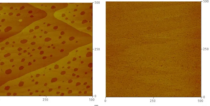
Figure 2.7. STM image of a dodecanethiol SAM made by immersing a gold bead in neat dodecanethiol (a) heated for 1 h at temperatures exceeding 100°C and (b) maintained at room temperature for 24 h.
Other experiments were done to probe the effect of concentration on the formation of a dodecanethiol SAM on gold. Contrary to some reports, it has been suggested that lower concentrations initiate less pit density and higher concentrations yield SAMs containing more pits.5 To probe the effect of lower concentrations, SAMs were fabricated by immersing annealed gold beads in solutions of dodecanethiol in ethanol at concentrations ranging from 1 µM to 100 µM under reflux for 1 h. Then, the sample was removed and put in a 1 mM solution of dodecanethiol in ethanol at room temperature for 15 min. These SAMs were briefly exposed to an elevated concentration of the adsorbent in order to ensure near
with less pit density compared to when 1 mM concentrations of the adsorbent were employed.
ethanol produced SAMs with significantly different pit densities. So, experiments were done where dodecanethiol SAMs were fabricated from both these concentrations according to the procedure outlined above. Before initiating replacement, relative humidity was set at 55% ± 2% and 4 µM of 11-ferrocenylundecanethioacetate (FcC11SAc) in dodecane was exposed to the substrate. Replacement lithography was performed on these SAMs by writing nine lines at biases from 2.5 V to 3.3 V (where the bias used to write each line was incrementally increased by 100 mV). After replacement lithography was done, STM images of these lines were captured at a scanning bias 1.5 V. Percent replacement was determined versus a
theoretical maximum according to procedure outlined in the experimental section. Figure 2.9 shows a STM image representative of what was observed when making a series of
replacement lithography lines composed of FcC11SAc in a dodecanethiol SAM made from a 0.01 mM solution of the adsorbent. Similar lines were observed in dodecanethiol SAMs made from a 1 mM solution of the adsorbent. Figure 2.10 shows a graph of percent
adsorbent yield SAMs with less pit density. Thus, it is concluded that an alkanethiol SAM on gold with lower pit density is more stable towards replacement lithography.
Figure 2.10. Graph of percent replacement versus bias used to make the replacement lithography lines
composed FcC11SAc. Percent replacement is shown at biases 2.6 V to 3.3 V.
2.5 Reducing Defects in SAMs Via an Alternate Vapor Deposition Procedure
Bumm et al. developed a method to deposit decanethiol SAMs on gold by vapor deposition.21 These researchers made these high quality SAMs by putting a gold substrate in a perfluoroalkoxy (PFA) inert vial with a few microliters of decanethiol, then sealing the sample in the vial and putting it in an oven set at 100°C for 12 h. It was claimed that the resulting SAMs were completely pit free.
Thus, experiments were done to explore what pit density could be created in decanethiol SAMs on gold beads and annealed gold on mica made following the above procedure. The above method was used to make decanethiol SAMs without pits, but it was hypothesized that similar results could be obtained later with SAMs composed of
Figure 2.11. STM image of a decanethiol SAM on a gold bead made from vapor deposition at 100°C for 12 h in a PFA vial.
Figure 2.12. STM image (250 x 250 nm) of decanethiol SAM made from vapor deposition at 100°C for 18 days in a PFA vial
2.6 Conclusions
decrease the pit density further or remove the pits completely by following a vapor
deposition method developed by Bumm et al. These experiments did yield slightly less pit densities in decanethiol SAMs on gold, but the pit density wasn’t significantly different compared to when 0.01 mM concentrations of alkanethiol were employed.
2.7 Experimental Section
General Considerations
Dodecanethiol and decanethiol were purchased from Alfa Aesar. Dodecane was purchased from Aldrich. Gold wire of 99.999% purity and 0.5 mm diameter was purchased from Alfa Aesar. PFA vials were purchased from Jensen Inert Products. Absolute ethanol was used as a solvent and was used without further purification. Gold on mica was
purchased from Novascan. FcC11SAc was synthesized in our laboratory following previously documented procedures.22 All water used was purified by reverse osmosis.
Preparation of Gold Surfaces
Caution! “Piranha” solution should be handled carefully because of its violent reactivity
with organic molecules.
Standard Solution Preparation of Dodecanethiol SAMs
SAMs of dodecanethiol were deposited by refluxing a freshly annealed gold bead ina 1 mM ethanol solution of the alkanethiol for 1 h followed by cooling of the solution to room temperature for 15 min. Then, the samples were rinsed with ethanol immediately after removing from the solution and dried under a stream of nitrogen.
Characterization
Scanning tunneling microscopy images were taken with a Nanoscope III (Digital instruments) after fixing the samples in a sample holder. These sample holders allowed one to scan with the sample submerged in a liquid solution of an ink. In experiments where pit density was explored, STM images were taken at 1.0 V sanning bias, 10 pA set point, and a scanning rate of 1 Hz. During experiments exploring percent replacement, images were taken at a capture bias of 1.5 V, 10 pA set point, and a scanning rate of 1 Hz.
Replacement Lithography
When relative humidity needed to be elevated, this was done by bubbling nitrogen through 18 MΩ·cm reverse osmosis water. Relative humidity was measured using a digital thermohydrometer.
Measuring Percent Replacement
2.8 References
(1) Love, J. C.; Estroff, L. A.; Kriebel, J. K.; Nuzzo, R. G.; Whitesides, G. M. Chem. Rev. (Washington, DC, U. S.)2005, 105, 1103-1169.
(2) Abdelghani, A. Mater. Lett.2001, 50, 73-77.
(3) Fuierer, R. R.; Carroll, R. L.; Feldheim, D. L.; Gorman, C. B. Adv. Mater. (Weinheim, Ger.)2002, 14, 154-157.
(4) Poirier, G. E. Chem. Rev. (Washington, DC, U. S.)1997, 97, 1117-1128.
(5) Vericat, C.; Vela, M. E.; Salvarezza, R. C. Phys. Chem. Chem. Phys.2005, 7,
3258-3268.
(6) Bucher, J. P.; Santesson, L.; Kern, K. Langmuir1994, 10, 979-983.
(7) Edinger, K.; Golzhauser, A.; Demota, K.; Woll, C.; Grunze, M. Langmuir1993, 9,
4-8.
(8) McCarley, R. L.; Dunaway, D. J.; Willicut, R. J. Langmuir1993, 9, 2775-2777.
(9) Poirier, G. E.; Tarlov, M. J. Langmuir1994, 10, 2853-2856.
(10) Schönenberger, C.; Sondag-Huethorst, J. A. M.; Jorritsma, J.; Fokkink, L. G. J.
Langmuir1994, 10, 611-614.
(11) Touzov, I.; Gorman, C. B. J. Phys. Chem. B1997, 101, 5263-5276.
(12) Leung, T. Y. B.; Gerstenberg, M. C.; Lavrich, D. J.; Scoles, G.; Schreiber, F.; Poirier, G. E. Langmuir2000, 16, 549-561.
(13) Gorman, C. B.; Carroll, R. L.; He, Y. F.; Tian, F.; Fuierer, R. Langmuir2000, 16,
6312-6316.
(14) Lewis, M. S.; Gorman, C. B. J. Phys. Chem. B2004, 108, 8581-8583.
(15) Williams, J.; Gorman, C. B. Langmuir2007, 23, 3103-3105.
(16) Cavalleri, O.; Hirstein, A.; Bucher, J.-P.; Kern, K. Thin Solid Films1996, 284,
392-395.
(17) Delamarche, E.; Michel, B.; Kang, H.; Gerber, C. Langmuir1994, 10, 4103-4108.
(19) Delamarche, E.; Michel, B.; Biebuyck, H. A.; Gerber, C. Adv. Mater. (Weinheim, Ger.)1996, 8, 719-729.
(20) Bumm, L. A.; Arnold, J. J.; Charles, L. F.; Dunbar, T. D.; Allara, D. L.; Weiss, P. S.
J. Am. Chem. Soc.1999, 121, 8017-8021.
(21) Bumm, L. A. In Unpublished Data; University of Oklahoma: Norman, Ok, 2008.
Chapter 3- GaAs AS A SUBSTRATE FOR REPLACEMENT LITHOGRAPHY
3.1 Introduction: Alkanethiol SAMs on GaAs
Gallium Arsenide (GaAs) has been commonly used in research and industry for applications in electronics and optoelectronics because of the interesting electronic properties of this substrate.1 In particular, this material has high electron mobilities. In addition, many reports have shown this material can act as a substrate for the formation of self-assembled monolayers (SAMs).1-5 SAMs, especially patterned SAMs, offer a convenient way to functionalize surfaces and could be employed to add useful functionality to GaAs. As
mentioned in previous chapters, the functionalization of substrates with interesting properties is important for many applications, such as construction of biosensors, solar cells, chemical sensors, etc.1,2,4
3.2 GaAs Surfaces Etched with HCl
3.2.1 Literature Precedent
Like many other semiconductor materials, GaAs is prone to forming an oxide layer upon exposure to air.1-5 Consequently, if one desires to work with an oxide free surface on this substrate, GaAs has to be treated with an etchant to remove the oxide layer. Most
preparation conditions use an acid as the etchant, especially concentrated HCl, but bases have also been used. This process precedes formation of any type of SAM that is intended to bind to GaAs (as opposed to an oxide of this material).
immersed in a solution of an alkanethiol at 100°C for 5 h to form the SAM. SAMs of HSCnH(2n+1), where n ranged from 12 to 22, were made on these surfaces. Also, SAMs composed of HSC15X, where X was either a carboxylic acid (-CO2H) or carboxylic acid methyl ester (-CO2CH3) were formed. The formation of the monolayer was confirmed using water contact angles and FTIR measurements. These techniques indicated the presence of a high surface coverage and densely packed SAM. The mechanics of the etching processes and amount of defects in the film were not elaborated on in this report, although later studies probed this more extensively.
One study employed AFM to probe the structure of freshly etched GaAs and
alkanethiol SAMs on GaAs.1 As mentioned previously, AFM and many SPM techniques are useful techniques for investigating defects and order at surfaces, especially in SAMs. Since the roughness of a surface affects the resulting order and amount of defects, surface
roughness during the etching of GaAs was devised. In addition, surface roughness was determined after deposition of the thiol SAMs on these surfaces to determine the quality of the films on GaAs treated with this optimal etching procedure. Using AFM, force-distance curves were taken on both the methyl terminated and alcohol terminated SAMs. The force-distance curves showed that the methyl terminated SAMs were, as expected, hydrophobic, and the alcohol terminated SAMs were hydrophilic. This observation helped confirm the presence of these SAMs and implied that they were of relatively high quality. However, all of the surface roughness and force curve measurements taken with AFM probed the surface at roughly the micrometer scale, so these measurements do not judge the ordering or surface roughness at the molecular scale.
The above report and others have investigated the mechanism of HCl etching and thiol SAM formation on GaAs.1 As mentioned above, Allara et al. proposed that the surface predominately consisted of arsenic upon HCl etching, but offered little support towards this claim.5 In the AFM study above, the authors proposed a more detailed mechanism,
suggesting HCl reacts readily with gallium, which causes it to be removed from the
surface.1,5 In addition, H+, provided by HCl, oxidizes the arsenide, but As+ remains present on the surface (Figure 3.1).1 It has been argued that the As+ has a high affinity for
occurs between gallium and the thiol.6,7 As a result, details about the bond that is formed between GaAs and the thiol as well as the mechanism of etching remain highly debated.
+ +
2
As + H
→
As + "1 2 H "
Figure 3.1. Proposed reaction for the etching of GaAs with HCl.1
Many of the reports mentioned above show strong evidence that high quality SAMs can be made using HCl to remove the native oxide layer prior to monolayer deposition.1,3,5 Since the techniques used in most of these reports to characterize these SAMs on GaAs measure an average of large areas of the surface, questions remain concerning the nanometer scale surface roughness of the substrate and the degree of crystallinity in these SAMs. Despite these concerns, it was desired to make alkanethiol SAMs on GaAs following treatment of the surface with HCl and apply replacement lithography to these surfaces.
3.2.2 Results and Discussion