Cyclone V Device Handbook
Volume 1: Device Interfaces and Integration
Contents
Logic Array Blocks and Adaptive Logic Modules in Cyclone V Devices... 1-1
LAB ... 1-1 MLAB ...1-2 Local and Direct Link Interconnects ...1-3 LAB Control Signals... 1-4 ALM Resources ... 1-5 ALM Output ... 1-6 ALM Operating Modes ... 1-8 Normal Mode ... 1-8 Extended LUT Mode ... 1-8 Arithmetic Mode ...1-8 Shared Arithmetic Mode ...1-9 Document Revision History...1-11
Embedded Memory Blocks in Cyclone V Devices... 2-1
Types of Embedded Memory... 2-1 Embedded Memory Capacity in Cyclone V Devices...2-1 Embedded Memory Design Guidelines for Cyclone V Devices...2-2 Guideline: Consider the Memory Block Selection... 2-2 Guideline: Implement External Conflict Resolution... 2-3 Guideline: Customize Read-During-Write Behavior... 2-3 Guideline: Consider Power-Up State and Memory Initialization... 2-7 Guideline: Control Clocking to Reduce Power Consumption...2-7 Embedded Memory Features... 2-7 Embedded Memory Configurations... 2-9 Mixed-Width Port Configurations...2-9 Embedded Memory Modes... 2-10 Embedded Memory Clocking Modes... 2-11 Clocking Modes for Each Memory Mode... 2-12 Asynchronous Clears in Clocking Modes... 2-12 Output Read Data in Simultaneous Read/Write...2-13 Independent Clock Enables in Clocking Modes... 2-13 Parity Bit in Memory Blocks... 2-13 Byte Enable in Embedded Memory Blocks... 2-14 Byte Enable Controls in Memory Blocks...2-14 Data Byte Output... 2-14 RAM Blocks Operations... 2-15 Memory Blocks Packed Mode Support... 2-15 Memory Blocks Address Clock Enable Support...2-15 Document Revision History...2-17
Variable Precision DSP Blocks in Cyclone V Devices...3-1
Features... 3-1 Supported Operational Modes in Cyclone V Devices... 3-2 Resources...3-3 Design Considerations... 3-4 Operational Modes... 3-4 Internal Coefficient and Pre-Adder...3-4 Accumulator... 3-4 Chainout Adder...3-4 Block Architecture... 3-5 Input Register Bank... 3-6 Pre-Adder...3-8 Internal Coefficient...3-8 Multipliers...3-9 Adder... 3-9 Accumulator and Chainout Adder...3-9 Systolic Registers...3-10 Double Accumulation Register...3-10 Output Register Bank...3-10 Operational Mode Descriptions... 3-11 Independent Multiplier Mode... 3-11 Independent Complex Multiplier Mode... 3-14 Multiplier Adder Sum Mode...3-16 18 x 18 Multiplication Summed with 36-Bit Input Mode...3-16 Systolic FIR Mode...3-16
Clock Networks and PLLs in Cyclone V Devices...4-1
Clock Networks...4-1 Clock Resources in Cyclone V Devices...4-2 Types of Clock Networks...4-4 Clock Sources Per Quadrant... 4-6 Types of Clock Regions...4-6 Clock Network Sources...4-7 Clock Output Connections...4-10 Clock Control Block... 4-10 Clock Power Down...4-11 Clock Enable Signals...4-12 Cyclone V PLLs...4-13
Clock Multiplication and Division...4-28 Programmable Phase Shift...4-29 Programmable Duty Cycle... 4-29 Clock Switchover... 4-30 PLL Reconfiguration and Dynamic Phase Shift... 4-35 Document Revision History...4-35
I/O Features in Cyclone V Devices...5-1
I/O Resources Per Package for Cyclone V Devices...5-1 I/O Vertical Migration for Cyclone V Devices... 5-4 Verifying Pin Migration Compatibility... 5-5 I/O Standards Support in Cyclone V Devices...5-6 I/O Standards Support for FPGA I/O in Cyclone V Devices... 5-6 I/O Standards Support for HPS I/O in Cyclone V Devices...5-7 I/O Standards Voltage Levels in Cyclone V Devices...5-8 MultiVolt I/O Interface in Cyclone V Devices... 5-10 I/O Design Guidelines for Cyclone V Devices...5-11 Mixing Voltage-Referenced and Non-Voltage-Referenced I/O Standards...5-11 PLLs and Clocking...5-12 LVDS Interface with External PLL Mode...5-14 Guideline: Use the Same VCCPD for All I/O Banks in a Group... 5-16
Guideline: Ensure Compatible VCCIO and VCCPD Voltage in the Same Bank... 5-17
Guideline: VREF Pin Restrictions... 5-17
Guideline: Observe Device Absolute Maximum Rating for 3.3 V Interfacing...5-17 Guideline: Adhere to the LVDS I/O Restrictions and Differential Pad Placement Rules... 5-18 Guideline: Pin Placement for General Purpose High-Speed Signals...5-18 I/O Banks Locations in Cyclone V Devices...5-18 I/O Banks Groups in Cyclone V Devices... 5-21 Modular I/O Banks for Cyclone V E Devices... 5-21 Modular I/O Banks for Cyclone V GX Devices...5-22 Modular I/O Banks for Cyclone V GT Devices...5-23 Modular I/O Banks for Cyclone V SE Devices... 5-24 Modular I/O Banks for Cyclone V SX Devices...5-25 Modular I/O Banks for Cyclone V ST Devices...5-26 I/O Element Structure in Cyclone V Devices... 5-26 I/O Buffer and Registers in Cyclone V Devices...5-26 Programmable IOE Features in Cyclone V Devices... 5-28 Programmable Current Strength...5-30 Programmable Output Slew-Rate Control...5-31 Programmable IOE Delay...5-32 Programmable Output Buffer Delay...5-32 Programmable Pre-Emphasis... 5-32 Programmable Differential Output Voltage... 5-33 Open-Drain Output...5-34 Bus-Hold Circuitry... 5-35 Pull-up Resistor...5-35 On-Chip I/O Termination in Cyclone V Devices...5-35 RS OCT without Calibration in Cyclone V Devices...5-36 TOC-4 Cyclone V Device Handbook Volume 1: Device Interfaces and Integration
RS OCT with Calibration in Cyclone V Devices...5-38 RT OCT with Calibration in Cyclone V Devices...5-40 Dynamic OCT in Cyclone V Devices...5-42 LVDS Input RD OCT in Cyclone V Devices...5-43
OCT Calibration Block in Cyclone V Devices...5-44 External I/O Termination for Cyclone V Devices...5-47 Single-ended I/O Termination...5-48 Differential I/O Termination... 5-50 Dedicated High-Speed Circuitries...5-55 High-Speed Differential I/O Locations...5-55 LVDS SERDES Circuitry... 5-58 True LVDS Buffers in Cyclone V Devices...5-59 Emulated LVDS Buffers in Cyclone V Devices... 5-67 Differential Transmitter in Cyclone V Devices... 5-67 Transmitter Blocks...5-67 Serializer Bypass for DDR and SDR Operations... 5-69 Differential Receiver in Cyclone V Devices... 5-69 Receiver Blocks in Cyclone V Devices...5-70 Receiver Mode in Cyclone V Devices... 5-71 Receiver Clocking for Cyclone V Devices... 5-71 Differential I/O Termination for Cyclone V Devices... 5-72 Source-Synchronous Timing Budget...5-72 Differential Data Orientation...5-73 Differential I/O Bit Position...5-73 Transmitter Channel-to-Channel Skew... 5-74 Receiver Skew Margin for Mode...5-75 Document Revision History...5-77
External Memory Interfaces in Cyclone V Devices... 6-1
External Memory Performance...6-1 HPS External Memory Performance...6-2 Memory Interface Pin Support in Cyclone V Devices...6-2 Guideline: Using DQ/DQS Pins... 6-2 DQ/DQS Bus Mode Pins for Cyclone V Devices... 6-3 DQ/DQS Groups in Cyclone V E... 6-4 DQ/DQS Groups in Cyclone V GX...6-6 DQ/DQS Groups in Cyclone V GT...6-8 DQ/DQS Groups in Cyclone V SE...6-9 DQ/DQS Groups in Cyclone V SX...6-10
Delay Chains...6-30 I/O and DQS Configuration Blocks... 6-32 Hard Memory Controller... 6-32 Features of the Hard Memory Controller... 6-33 Multi-Port Front End ... 6-35 Bonding Support...6-36 Hard Memory Controller Width for Cyclone V E...6-36 Hard Memory Controller Width for Cyclone V GX... 6-37 Hard Memory Controller Width for Cyclone V GT... 6-37 Hard Memory Controller Width for Cyclone V SE...6-38 Hard Memory Controller Width for Cyclone V SX... 6-39 Hard Memory Controller Width for Cyclone V ST...6-39 Document Revision History...6-40
Configuration, Design Security, and Remote System Upgrades in Cyclone V
Devices... 7-1
Enhanced Configuration and Configuration via Protocol...7-1 MSEL Pin Settings...7-2 Configuration Sequence...7-3 Power Up...7-4 Reset...7-5 Configuration... 7-5 Configuration Error Handling...7-6 Initialization...7-6 User Mode...7-6 Configuration Timing Waveforms...7-7 FPP Configuration Timing...7-7 AS Configuration Timing... 7-9 PS Configuration Timing...7-10 Device Configuration Pins... 7-10 I/O Standards and Drive Strength for Configuration Pins...7-11 Configuration Pin Options in the Quartus Prime Software... 7-11 Fast Passive Parallel Configuration... 7-12 Fast Passive Parallel Single-Device Configuration...7-12 Fast Passive Parallel Multi-Device Configuration...7-13 Transmitting Configuration Data... 7-15 Active Serial Configuration...7-16 DATA Clock (DCLK)...7-16 Active Serial Single-Device Configuration...7-16 Active Serial Multi-Device Configuration...7-18 Estimating the Active Serial Configuration Time... 7-19 Using EPCS and EPCQ Devices... 7-19 Controlling EPCS and EPCQ Devices... 7-20 Trace Length and Loading Guideline...7-20 Programming EPCS and EPCQ Devices... 7-20 Passive Serial Configuration...7-24 Passive Serial Single-Device Configuration Using an External Host... 7-25 Passive Serial Single-Device Configuration Using an Altera Download Cable... 7-25
Passive Serial Multi-Device Configuration... 7-26 JTAG Configuration...7-29 JTAG Single-Device Configuration...7-30 JTAG Multi-Device Configuration... 7-31 CONFIG_IO JTAG Instruction...7-32 Configuration Data Compression... 7-33 Enabling Compression Before Design Compilation...7-33 Enabling Compression After Design Compilation...7-33 Using Compression in Multi-Device Configuration... 7-33 Remote System Upgrades... 7-34 Configuration Images...7-35 Configuration Sequence in the Remote Update Mode...7-36 Remote System Upgrade Circuitry...7-36 Enabling Remote System Upgrade Circuitry...7-37 Remote System Upgrade Registers...7-37 Remote System Upgrade State Machine...7-39 User Watchdog Timer...7-39 Design Security...7-40 Altera Unique Chip ID IP Core... 7-41 JTAG Secure Mode...7-41 Security Key Types...7-41 Security Modes... 7-42 Design Security Implementation Steps...7-43 Document Revision History...7-43
SEU Mitigation for Cyclone V Devices... 8-1
Error Detection Features...8-1 Configuration Error Detection... 8-1 User Mode Error Detection...8-1 Internal Scrubbing... 8-2 Specifications...8-2 Minimum EMR Update Interval... 8-2 Error Detection Frequency...8-3 CRC Calculation Time For Entire Device... 8-3 Using Error Detection Features in User Mode...8-3 Enabling Error Detection...8-3 CRC_ERROR Pin...8-4 Error Detection Registers...8-4 Error Detection Process... 8-6
JTAG Private Instruction ...9-6 I/O Voltage for JTAG Operation ...9-6 Performing BST ...9-7 Enabling and Disabling IEEE Std. 1149.1 BST Circuitry ... 9-7 Guidelines for IEEE Std. 1149.1 Boundary-Scan Testing...9-8 IEEE Std. 1149.1 Boundary-Scan Register ...9-8 Boundary-Scan Cells of a Cyclone V Device I/O Pin... 9-9 Document Revision History...9-11
Power Management in Cyclone V Devices... 10-1
Power Consumption...10-1 Dynamic Power Equation...10-1 Hot-Socketing Feature... 10-2 Hot-Socketing Implementation...10-2 Power-Up Sequence... 10-4 Power-On Reset Circuitry... 10-5 Power Supplies Monitored and Not Monitored by the POR Circuitry... 10-6 Document Revision History...10-7
Logic Array Blocks and Adaptive Logic Modules
in Cyclone V Devices
1
2015.12.21
CV-52001 Subscribe Send Feedback
This chapter describes the features of the logic array block (LAB) in the Cyclone® V core fabric.
The LAB is composed of basic building blocks known as adaptive logic modules (ALMs) that you can configure to implement logic functions, arithmetic functions, and register functions.
You can use a quarter of the available LABs in the Cyclone V devices as a memory LAB (MLAB). The Quartus® Prime software and other supported third-party synthesis tools, in conjunction with
parameterized functions such as the library of parameterized modules (LPM), automatically choose the appropriate mode for common functions such as counters, adders, subtractors, and arithmetic functions. This chapter contains the following sections:
• LAB
• ALM Operating Modes
Related Information
Cyclone V Device Handbook: Known Issues
Lists the planned updates to the Cyclone V Device Handbook chapters.
LAB
The LABs are configurable logic blocks that consist of a group of logic resources. Each LAB contains dedicated logic for driving control signals to its ALMs.
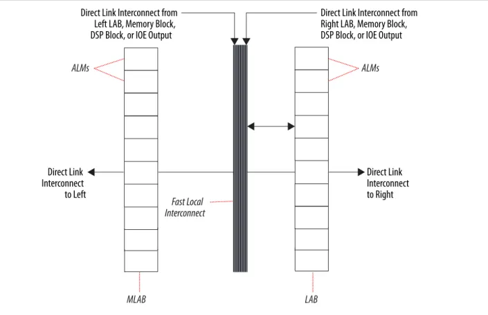
Figure 1-1: LAB Structure and Interconnects Overview in Cyclone V Devices
This figure shows an overview of the Cyclone V LAB and MLAB structure with the LAB interconnects.
Fast Local Interconnect Is Driven from Either Sides by Column Interconnect and LABs, and from Above by Row Interconnect
Column Interconnects of Variable Speed and Length Row Interconnects of
Variable Speed and Length
MLAB LAB Local Interconnect ALMs C2/C4 C12 R14 R3/R6 Direct-Link Interconnect from Adjacent Block Direct-Link Interconnect to Adjacent Block Direct-Link Interconnect to Adjacent Block Direct-Link Interconnect from Adjacent Block Connects to adjacent LABs, memory blocks, digital signal processing
(DSP) blocks, or I/O element (IOE) outputs.
MLAB
Each MLAB supports a maximum of 640 bits of simple dual-port SRAM.
Figure 1-2: LAB and MLAB Structure for Cyclone V Devices
MLAB LAB
LUT-Based-32 x 2 Simple Dual-Port SRAM
LUT-Based-32 x 2 Simple Dual-Port SRAM
LUT-Based-32 x 2 Simple Dual-Port SRAM
LUT-Based-32 x 2 Simple Dual-Port SRAM
LUT-Based-32 x 2 Simple Dual-Port SRAM
LUT-Based-32 x 2 Simple Dual-Port SRAM
LUT-Based-32 x 2 Simple Dual-Port SRAM
LUT-Based-32 x 2 Simple Dual-Port SRAM
LUT-Based-32 x 2 Simple Dual-Port SRAM
LUT-Based-32 x 2 Simple Dual-Port SRAM
ALM ALM ALM ALM ALM ALM ALM ALM ALM ALM LAB Control Block LAB Control Block
You can use an MLAB ALM as a regular LAB ALM or configure it as a dual-port SRAM.
You can use an MLAB ALM as a regular LAB ALM or configure it as a dual-port SRAM.
Local and Direct Link Interconnects
Each LAB can drive 30 ALMs through fast-local and direct-link interconnects. Ten ALMs are in any given LAB and ten ALMs are in each of the adjacent LABs.
The local interconnect can drive ALMs in the same LAB using column and row interconnects and ALM outputs in the same LAB.
Neighboring LABs, MLABs, M10K blocks, or digital signal processing (DSP) blocks from the left or right
CV-52001
Figure 1-3: LAB Fast Local and Direct Link Interconnects for Cyclone V Devices MLAB ALMs ALMs LAB Fast Local Interconnect
Direct Link Interconnect from Left LAB, Memory Block, DSP Block, or IOE Output
Direct Link Interconnect to Left Direct Link Interconnect to Right Direct Link Interconnect from Right LAB, Memory Block, DSP Block, or IOE Output
LAB Control Signals
Each LAB contains dedicated logic for driving the control signals to its ALMs, and has two unique clock sources and three clock enable signals.
The LAB control block generates up to three clocks using the two clock sources and three clock enable signals. Each clock and the clock enable signals are linked.
De-asserting the clock enable signal turns off the corresponding LAB-wide clock.
Figure 1-4: LAB-Wide Control Signals for Cyclone V Devices
This figure shows the clock sources and clock enable signals in a LAB.
Dedicated Row LAB Clocks Local Interconnect Local Interconnect Local Interconnect Local Interconnect labclk2 syncload labclkena0 or asyncload or labpreset
labclk0 labclk1 labclr1
labclkena1 labclkena2 labclr0 synclr
6 6 6
There are two unique clock signals per LAB.
ALM Resources
One ALM contains four programmable registers. Each register has the following ports: • Data
• Clock
• Synchronous and asynchronous clear • Synchronous load
Global signals, general-purpose I/O (GPIO) pins, or any internal logic can drive the clock and clear control signals of an ALM register.
CV-52001
Figure 1-5: ALM High-Level Block Diagram for Cyclone V Devices datac datad datae1 dataf1 adder1 datae0 dataf0 dataa datab carry_in carry_out Combinational/ Memory ALUT0 6-Input LUT 6-Input LUT shared_arith_out shared_arith_in Combinational/ Memory ALUT1 adder0 reg0 labclk reg1 reg2 reg3 D Q D Q D Q D Q To General or Local Routing
ALM Output
The general routing outputs in each ALM drive the local, row, and column routing resources. Two ALM outputs can drive column, row, or direct link routing connections, and one of these ALM outputs can also drive local interconnect resources.
The LUT, adder, or register output can drive the ALM outputs. The LUT or adder can drive one output while the register drives another output.
Register packing improves device utilization by allowing unrelated register and combinational logic to be packed into a single ALM. Another mechanism to improve fitting is to allow the register output to feed back into the look-up table (LUT) of the same ALM so that the register is packed with its own fan-out LUT. The ALM can also drive out registered and unregistered versions of the LUT or adder output.
Figure 1-6: ALM Connection Details for Cyclone V Devices
D CLRQ D CLRQ
Row, Column Direct Link Routing
D CLRQ Local Interconnect Local Interconnect D CLRQ carry_out GND VCC aclr[1:0] sclr syncload clk[2:0] carry_in + shared_arith_out shared_arith_in 4-Input LUT 4-Input LUT 3-Input LUT 3-Input LUT 3-Input LUT 3-Input LUT + dataf0 datae0 dataa datab datac1 datae1 dataf1 datac0 Row, Column Direct Link Routing
Row, Column Direct Link Routing
Row, Column Direct Link Routing
CV-52001
ALM Operating Modes
The Cyclone V ALM operates in any of the following modes: • Normal mode
• Extended LUT mode • Arithmetic mode • Shared arithmetic mode
Normal Mode
Normal mode allows two functions to be implemented in one Cyclone V ALM, or a single function of up to six inputs.
Up to eight data inputs from the LAB local interconnect are inputs to the combinational logic.
The ALM can support certain combinations of completely independent functions and various combina‐ tions of functions that have common inputs.
Extended LUT Mode
In this mode, if the 7-input function is unregistered, the unused eighth input is available for register packing.
Functions that fit into the template, as shown in the following figure, often appear in designs as “if-else” statements in Verilog HDL or VHDL code.
Figure 1-7: Template for Supported 7-Input Functions in Extended LUT Mode for Cyclone V Devices
datae0 combout0 5-Input LUT 5-Input LUT datac dataa datab datad dataf0 datae1 dataf1 D Q reg0
This input is available for register packing.
To General or Local Routing
Arithmetic Mode
The ALM in arithmetic mode uses two sets of two 4-input LUTs along with two dedicated full adders. The dedicated adders allow the LUTs to perform pre-adder logic; therefore, each adder can add the output of two 4-input functions.
The ALM supports simultaneous use of the adder’s carry output along with combinational logic outputs. The adder output is ignored in this operation.
Using the adder with the combinational logic output provides resource savings of up to 50% for functions that can use this mode.
Figure 1-8: ALM in Arithmetic Mode for Cyclone V Devices
datae0 carry_in carry_out dataa databdatac datad datae1 4-Input LUT 4-Input LUT 4-Input LUT 4-Input LUT adder1 dataf0 dataf1 adder0 reg1 To General or Local Routing reg0 reg3 reg2 Carry Chain
The carry chain provides a fast carry function between the dedicated adders in arithmetic or shared arithmetic mode.
The two-bit carry select feature in Cyclone V devices halves the propagation delay of carry chains within the ALM. Carry chains can begin in either the first ALM or the fifth ALM in a LAB. The final carry-out signal is routed to an ALM, where it is fed to local, row, or column interconnects.
To avoid routing congestion in one small area of the device when a high fan-in arithmetic function is implemented, the LAB can support carry chains that only use either the top half or bottom half of the LAB before connecting to the next LAB. This leaves the other half of the ALMs in the LAB available for
implementing narrower fan-in functions in normal mode. Carry chains that use the top five ALMs in the first LAB carry into the top half of the ALMs in the next LAB in the column. Carry chains that use the bottom five ALMs in the first LAB carry into the bottom half of the ALMs in the next LAB within the
CV-52001
This mode configures the ALM with four 4-input LUTs. Each LUT either computes the sum of three inputs or the carry of three inputs. The output of the carry computation is fed to the next adder using a dedicated connection called the shared arithmetic chain.
Figure 1-9: ALM in Shared Arithmetic Mode for Cyclone V Devices
datae0 carry_in shared_arith_in shared_arith_out carry_out dataa databdatac datad datae1 4-Input LUT 4-Input LUT 4-Input LUT 4-Input LUT labclk reg1 To General or Local Routing reg0 reg3 reg2
Shared Arithmetic Chain
The shared arithmetic chain available in enhanced arithmetic mode allows the ALM to implement a 3-input adder. This significantly reduces the resources necessary to implement large adder trees or correlator functions.
The shared arithmetic chain can begin in either the first or sixth ALM in a LAB.
Similar to carry chains, the top and bottom half of the shared arithmetic chains in alternate LAB columns can be bypassed. This capability allows the shared arithmetic chain to cascade through half of the ALMs in an LAB while leaving the other half available for narrower fan-in functionality. In every LAB, the column is top-half bypassable; while in MLAB, columns are bottom-half bypassable.
The Quartus Prime Compiler creates shared arithmetic chains longer than 20 ALMs (10 ALMs in
arithmetic or shared arithmetic mode) by linking LABs together automatically. To enhance fitting, a long shared arithmetic chain runs vertically, allowing fast horizontal connections to the TriMatrix memory and DSP blocks. A shared arithmetic chain can continue as far as a full column.
Document Revision History
Date Version Changes
December
2015 2015.12.21 Changed instances of Quartus II to Quartus Prime.
January 2014 2014.01.10 Added multiplexers for the bypass paths and register outputs in the following diagrams:
• ALM High-Level Block Diagram for Cyclone V Devices
• Template for Supported 7-Input Functions in Extended LUT Mode for Cyclone V Devices
• ALM in Arithmetic Mode for Cyclone V Devices • ALM in Shared Arithmetic Mode for Cyclone V Devices
May 2013 2013.05.06 • Added link to the known document issues in the Knowledge Base. • Removed register chain outputs information in ALM output section. • Removed reg_chain_in and reg_chain_out ports in ALM
high-level block diagram and ALM connection details diagram. December
2012 2012.12.28 Reorganized content and updated template. June 2012 2.0 Updated for the Quartus II software v12.0 release:
• Restructured chapter. • Updated Figure 1–6. November
2011 1.1 Minor text edits. October 2011 1.0 Initial release.
CV-52001
Embedded Memory Blocks in Cyclone V
Devices
2
2015.12.21
CV-52002 Subscribe Send Feedback
The embedded memory blocks in the devices are flexible and designed to provide an optimal amount of small- and large-sized memory arrays to fit your design requirements.
Related Information
Cyclone V Device Handbook: Known Issues
Lists the planned updates to the Cyclone V Device Handbook chapters.
Types of Embedded Memory
The Cyclone V devices contain two types of memory blocks:
• 10 Kb M10K blocks—blocks of dedicated memory resources. The M10K blocks are ideal for larger memory arrays while still providing a large number of independent ports.
• 640 bit memory logic array blocks (MLABs)—enhanced memory blocks that are configured from dual-purpose logic array blocks (LABs). The MLABs are ideal for wide and shallow memory arrays. The MLABs are optimized for implementation of shift registers for digital signal processing (DSP) applica‐ tions, wide shallow FIFO buffers, and filter delay lines. Each MLAB is made up of ten adaptive logic modules (ALMs). In the Cyclone V devices, you can configure these ALMs as ten 32 x 2 blocks, giving you one 32 x 20 simple dual-port SRAM block per MLAB.
Embedded Memory Capacity in Cyclone V Devices
Table 2-1: Embedded Memory Capacity and Distribution in Cyclone V Devices
Variant MemberCode
M10K MLAB
Total RAM Bit (Kb)
Block RAM Bit (Kb) Block RAM Bit (Kb)
Cyclone V E A2 176 1,760 314 196 1,956 A4 308 3,080 485 303 3,383 A5 446 4,460 679 424 4,884 A7 686 6,860 1338 836 7,696 A9 1,220 12,200 2748 1,717 13,917
© 2015 Altera Corporation. All rights reserved. ALTERA, ARRIA, CYCLONE, ENPIRION, MAX, MEGACORE, NIOS, QUARTUS and STRATIX words and logos are
trademarks of Altera Corporation and registered in the U.S. Patent and Trademark Office and in other countries. All other words and logos identified as trademarks or service marks are the property of their respective holders as described at www.altera.com/common/legal.html. Altera warrants performance of its semiconductor products to current specifications in accordance with Altera's standard warranty, but reserves the right to make changes to any
ISO 9001:2008
Variant MemberCode
M10K MLAB
Total RAM Bit (Kb)
Block RAM Bit (Kb) Block RAM Bit (Kb)
Cyclone V GX C3 135 1,350 291 182 1,532 C4 250 2,500 678 424 2,924 C5 446 4,460 678 424 4,884 C7 686 6,860 1338 836 7,696 C9 1,220 12,200 2748 1,717 13,917 Cyclone V GT D5 446 4,460 679 424 4,884 D7 686 6,860 1338 836 7,696 D9 1,220 12,200 2748 1,717 13,917 Cyclone V SE A2 140 1,400 221 138 1,538 A4 270 2,700 370 231 2,460 A5 397 3,970 768 480 4,450 A6 557 5,570 994 621 5,761 Cyclone V SX C2 140 1,400 221 138 1,538 C4 270 2,700 370 231 2,460 C5 397 3,970 768 480 4,450 C6 557 5,570 994 621 5,761 Cyclone V ST D5 397 3,970 768 480 4,450 D6 557 5,570 994 621 5,761
Embedded Memory Design Guidelines for Cyclone V Devices
There are several considerations that require your attention to ensure the success of your designs. Unless noted otherwise, these design guidelines apply to all variants of this device family.
Guideline: Consider the Memory Block Selection
The Quartus Prime software automatically partitions the user-defined memory into the memory blocks based on your design's speed and size constraints. For example, the Quartus Prime software may spread out the memory across multiple available memory blocks to increase the performance of the design.
Guideline: Implement External Conflict Resolution
In the true dual-port RAM mode, you can perform two write operations to the same memory location. However, the memory blocks do not have internal conflict resolution circuitry. To avoid unknown data being written to the address, implement external conflict resolution logic to the memory block.
Guideline: Customize Read-During-Write Behavior
Customize the read-during-write behavior of the memory blocks to suit your design requirements.
Figure 2-1: Read-During-Write Data Flow
This figure shows the difference between the two types of read-during-write operations available—same port and mixed port.
Port A
data in Port Bdata in
Port A
data out Port Bdata out
Mixed-port data flow Same-port data flow FPGA Device
Same-Port Read-During-Write Mode
The same-port read-during-write mode applies to a single-port RAM or the same port of a true dual-port RAM.
Table 2-2: Output Modes for Embedded Memory Blocks in Same-Port Read-During-Write Mode
This table lists the available output modes if you select the embedded memory blocks in the same-port read-during-write mode.
Output Mode Memory Type Description
"new data" (flow-through)
M10K The new data is available on the rising edge of the same clock cycle on which the new data is written.
"don't care" M10K, MLAB The RAM outputs "don't care" values for a read-during-write operation.
CV-52002
Figure 2-2: Same-Port Read-During-Write: New Data Mode
This figure shows sample functional waveforms of same-port read-during-write behavior in the “new data” mode. clk_a address rden wren byteena data_a q_a (asynch) A123 B456 C789 DDDD EEEE FFFF A123 B456 C789 DDDD EEEE FFFF 0A 0B 11
Mixed-Port Read-During-Write Mode
The mixed-port read-during-write mode applies to simple and true dual-port RAM modes where two ports perform read and write operations on the same memory address using the same clock—one port reading from the address, and the other port writing to it.
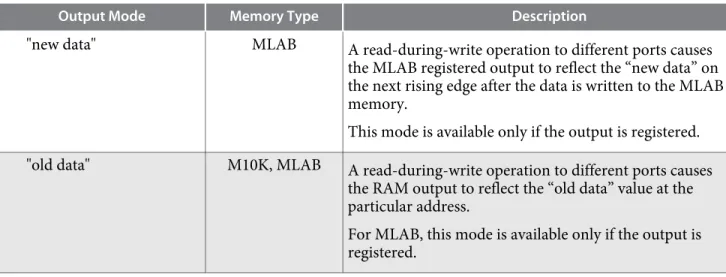
Table 2-3: Output Modes for RAM in Mixed-Port Read-During-Write Mode
Output Mode Memory Type Description
"new data" MLAB A read-during-write operation to different ports causes the MLAB registered output to reflect the “new data” on the next rising edge after the data is written to the MLAB memory.
This mode is available only if the output is registered. "old data" M10K, MLAB A read-during-write operation to different ports causes
the RAM output to reflect the “old data” value at the particular address.
For MLAB, this mode is available only if the output is registered.
Output Mode Memory Type Description
"don't care" M10K, MLAB The RAM outputs “don’t care” or “unknown” value. • For M10K memory, the Quartus Prime software does
not analyze the timing between write and read operations.
• For MLAB, the Quartus Prime software analyzes the timing between write and read operations by default. To disable this behavior, turn on the Do not analyze
the timing between write and read operation. Metastability issues are prevented by never writing and reading at the same address at the same time
option.
"constrained don't care" MLAB The RAM outputs “don’t care” or “unknown” value. The Quartus Prime software analyzes the timing between write and read operations in the MLAB.
Figure 2-3: Mixed-Port Read-During-Write: New Data Mode
This figure shows a sample functional waveform of mixed-port read-during-write behavior for the “new data” mode. XXXX 11 clk_a&b address_a wren_a byteena_a rden_b data_a q_b (registered) address_b AAAA BBBB CCCC DDDD EEEE FFFF A0 A1 A0 A1 AAAA BBBB CCCC DDDD EEEE FFFF CV-52002
Figure 2-4: Mixed-Port Read-During-Write: Old Data Mode
This figure shows a sample functional waveform of mixed-port read-during-write behavior for the “old data” mode. XXXX 11 clk_a&b address_a wren_a byteena_a rden_b data_a q_b (registered) address_b AAAA BBBB CCCC DDDD EEEE FFFF A0 A1 A0 A1
AAAA BBBB A1 (old data) DDDD EEEE A0 (old data)
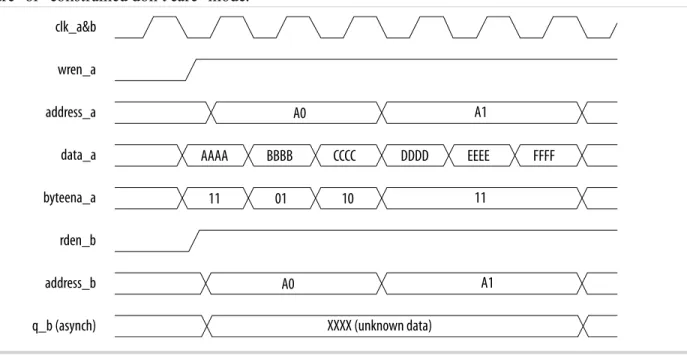
Figure 2-5: Mixed-Port Read-During-Write: Don’t Care or Constrained Don’t Care Mode
This figure shows a sample functional waveform of mixed-port read-during-write behavior for the “don’t care” or “constrained don’t care” mode.
clk_a&b wren_a address_a A0 A1 data_a byteena_a rden_b address_b
q_b (asynch) XXXX (unknown data)
A0 A1
11 01 10 11
AAAA BBBB CCCC DDDD EEEE FFFF
Guideline: Consider Power-Up State and Memory Initialization
Consider the power up state of the different types of memory blocks if you are designing logic that evaluates the initial power-up values, as listed in the following table.
Table 2-4: Initial Power-Up Values of Embedded Memory Blocks
Memory Type Output Registers Power Up Value
MLAB Used Zero (cleared)
Bypassed Read memory contents
M10K Used Zero (cleared)
Bypassed Zero (cleared)
By default, the Quartus Prime software initializes the RAM cells in Cyclone V devices to zero unless you specify a .mif.
All memory blocks support initialization with a .mif. You can create .mif files in the Quartus Prime software and specify their use with the RAM IP core when you instantiate a memory in your design. Even if a memory is pre-initialized (for example, using a .mif), it still powers up with its output cleared.
Related Information
• Embedded Memory (RAM: 1-PORT, RAM:2-PORT, ROM: 1-PORT, and ROM: 2-PORT) User
Guide
Provides more information about .mif files.
• Quartus II Handbook
Provides more information about .mif files.
Guideline: Control Clocking to Reduce Power Consumption
Reduce AC power consumption in your design by controlling the clocking of each memory block: • Use the read-enable signal to ensure that read operations occur only when necessary. If your design
does not require during-write, you can reduce your power consumption by de-asserting the read-enable signal during write operations, or during the period when no memory operations occur.
• Use the Quartus Prime software to automatically place any unused memory blocks in low-power mode to reduce static power.
Embedded Memory Features
Table 2-5: Memory Features in Cyclone V Devices
This table summarizes the features supported by the embedded memory blocks.
Features M10K MLAB
Maximum operating frequency
Capacity per block (including parity bits) 640
CV-52002
Features M10K MLAB
Parity bits Supported Supported
Byte enable Supported Supported
Packed mode Supported —
Address clock enable Supported Supported
Simple dual-port mixed width Supported —
True dual-port mixed width Supported —
FIFO buffer mixed width Supported —
Memory Initialization File (.mif) Supported Supported
Mixed-clock mode Supported Supported
Fully synchronous memory Supported Supported
Asynchronous memory — Only for flow-through read memory operations. Power-up state Output ports are
cleared. • Registered output ports—Cleared. • Unregistered output ports—
Read memory contents. Asynchronous clears Output registers and
output latches Output registers and outputlatches Write/read operation triggering Rising clock edges Rising clock edges
Same-port read-during-write (The "don't care" mode applies only for the single-port RAM mode).
Output ports set to "don't care".
Mixed-port read-during-write Output ports set to "old data" or "don't care".
Output ports set to "old data", "new data", "don't care", or "constrained don't care".
ECC support Soft IP support using the Quartus Prime software.
Soft IP support using the Quartus Prime software.
Embedded Memory Configurations
Table 2-6: Supported Embedded Memory Block Configurations for Cyclone V Devices
This table lists the maximum configurations supported for the embedded memory blocks. The information is applicable only to the single-port RAM and ROM modes.
Memory Block Depth (bits) Programmable Width
M10K 256 x40 or x32 512 x20 or x16 1K x10 or x8 2K x5 or x4 4K x2 8K x1
Mixed-Width Port Configurations
The mixed-width port configuration is supported in the simple dual-port RAM and true dual-port RAM memory modes.
Note: MLABs do not support mixed-width port configurations.
Related Information
Embedded Memory (RAM: 1-PORT, RAM:2-PORT, ROM: 1-PORT, and ROM: 2-PORT) User Guide
Provides more information about dual-port mixed width support.
M10K Blocks Mixed-Width Configurations
Table 2-7: M10K Block Mixed-Width Configurations in Simple Dual-Port RAM Mode Read Port
Write Port
8K x 1 4K x 2 2K x 4 2K x 5 1K x 8 1k x 10 512 x 1
6 512 x 20 256 x 32 256 x 40
8K x 1 Yes Yes Yes — Yes — Yes — Yes —
4K x 2 Yes Yes Yes — Yes — Yes — Yes —
2K x 4 Yes Yes Yes — Yes — Yes — Yes —
2K x 5 — — — Yes — Yes — Yes — Yes
1K x 8 Yes Yes Yes — Yes — Yes — Yes —
1K x 10 — — — Yes — Yes — Yes — Yes
512 x 16 Yes Yes Yes — Yes — Yes — Yes —
512 x 20 — — — Yes — Yes — Yes — Yes
256 x 32 Yes Yes Yes — Yes — Yes — Yes —
256 x 40 — — — Yes — Yes — Yes — Yes
CV-52002
Table 2-8: M10K Block Mixed-Width Configurations in True Dual-Port Mode
Port B Port A
8K x 1 4K x 2 2K x 4 2K x 5 1K x 8 1K x 10 512 x 16 512 x 20
8K x 1 Yes Yes Yes — Yes — Yes —
4K x 2 Yes Yes Yes — Yes — Yes —
2K x 4 Yes Yes Yes — Yes — Yes —
2K x 5 — — — Yes — Yes — Yes
1K x 8 Yes Yes Yes — Yes — Yes —
1K x 10 — — — Yes — Yes — Yes
512 x 16 Yes Yes Yes — Yes — Yes —
512 x 20 — — — Yes — Yes — Yes
Embedded Memory Modes
Caution: To avoid corrupting the memory contents, do not violate the setup or hold time on any of the memory block input registers during read or write operations. This is applicable if you use the memory blocks in single-port RAM, simple dual-port RAM, true dual-port RAM, or ROM mode.
Table 2-9: Memory Modes Supported in the Embedded Memory Blocks
This table lists and describes the memory modes that are supported in the Cyclone V embedded memory blocks.
Memory Mode SupportM10K SupportMLAB Description
Single-port RAM Yes Yes You can perform only one read or one write operation at a time.
Use the read enable port to control the RAM output ports behavior during a write operation:
• To retain the previous values that are held during the most recent active read enable—create a read-enable port and perform the write operation with the read enable port deasserted.
• To show the new data being written, the old data at that address, or a "Don't Care" value when read-during-write
Memory Mode SupportM10K SupportMLAB Description
True dual-port
RAM Yes — You can perform any combination of two port operations: tworeads, two writes, or one read and one write at two different clock frequencies.
Shift-register Yes Yes You can use the memory blocks as a shift-register block to save logic cells and routing resources.
This is useful in DSP applications that require local data storage such as finite impulse response (FIR) filters, pseudo-random number generators, multi-channel filtering, and auto- and cross- correlation functions. Traditionally, the local data storage is implemented with standard flip-flops that exhaust many logic cells for large shift registers.
The input data width (w), the length of the taps (m), and the number of taps (n) determine the size of a shift register (w × m × n). You can cascade memory blocks to implement larger shift registers.
ROM Yes Yes You can use the memory blocks as ROM.
• Initialize the ROM contents of the memory blocks using a .mif or .hex.
• The outputs can be registered or unregistered. • The output registers can be asynchronously cleared. • The ROM read operation is identical to the read operation
in the single-port RAM configuration.
FIFO Yes Yes You can use the memory blocks as FIFO buffers. Use the SCFIFO and DCFIFO IP cores to implement single- and dual-clock asynchronous FIFO buffers in your design.
For designs with many small and shallow FIFO buffers, the MLABs are ideal for the FIFO mode. However, the MLABs do not support mixed-width FIFO mode.
Related Information
• Embedded Memory (RAM: 1-PORT, RAM:2-PORT, ROM: 1-PORT, and ROM: 2-PORT) User
Guide
Provides more information memory modes.
• RAM-Based Shift Register (ALTSHIFT_TAPS) IP Core User Guide
Provides more information about implementing the shift register mode.
• SCFIFO and DCFIFO IP Cores User Guide
Provides more information about implementing FIFO buffers.
Embedded Memory Clocking Modes
This section describes the clocking modes for the Cyclone V memory blocks.
CV-52002
Caution: To avoid corrupting the memory contents, do not violate the setup or hold time on any of the memory block input registers during read or write operations.
Clocking Modes for Each Memory Mode
Table 2-10: Memory Blocks Clocking Modes Supported for Each Memory Mode Clocking Mode
Memory Mode
Single-Port Simple
Dual-Port True Dual-Port ROM FIFO
Single clock mode Yes Yes Yes Yes Yes
Read/write clock mode — Yes — — Yes
Input/output clock mode Yes Yes Yes Yes —
Independent clock mode — — Yes Yes —
Note: The clock enable signals are not supported for write address, byte enable, and data input registers
on MLAB blocks.
Single Clock Mode
In the single clock mode, a single clock, together with a clock enable, controls all registers of the memory block.
Read/Write Clock Mode
In the read/write clock mode, a separate clock is available for each read and write port. A read clock controls the data-output, read-address, and read-enable registers. A write clock controls the data-input, write-address, write-enable, and byte enable registers.
Input/Output Clock Mode
In input/output clock mode, a separate clock is available for each input and output port. An input clock controls all registers related to the data input to the memory block including data, address, byte enables, read enables, and write enables. An output clock controls the data output registers.
Independent Clock Mode
In the independent clock mode, a separate clock is available for each port (A and B). Clock A controls all registers on the port A side; clock B controls all registers on the port B side.
Output Read Data in Simultaneous Read/Write
If you perform a simultaneous read/write to the same address location using the read/write clock mode, the output read data is unknown. If you require the output read data to be a known value, use single-clock or input/output clock mode and select the appropriate read-during-write behavior in the IP Catalog.
Note: MLAB memory blocks only support simultaneous read/write operations when operating in single
clock mode.
Independent Clock Enables in Clocking Modes
Independent clock enables are supported in the following clocking modes: • Read/write clock mode—supported for both the read and write clocks. • Independent clock mode—supported for the registers of both ports.
To save power, you can control the shut down of a particular register using the clock enables.
Related Information
Guideline: Control Clocking to Reduce Power Consumption on page 2-7
Parity Bit in Memory Blocks
Table 2-11: Parity Bit Support for the Embedded Memory Blocks
This table describes the parity bit support for the memory blocks.
M10K MLAB
• The parity bit is the fifth bit associated with each 4 data bits in data widths of 5, 10, 20, and 40 (bits 4, 9, 14, 19, 24, 29, 34, and 39).
• In non-parity data widths, the parity bits are skipped during read or write operations. • Parity function is not performed on the parity
bit.
• The parity bit is the ninth bit associated with each byte.
• The ninth bit can store a parity bit or serve as an additional bit.
• Parity function is not performed on the parity bit.
CV-52002
Byte Enable in Embedded Memory Blocks
The embedded memory blocks support byte enable controls:
• The byte enable controls mask the input data so that only specific bytes of data are written. The unwritten bytes retain the values written previously.
• The write enable (wren) signal, together with the byte enable (byteena) signal, control the write
operations on the RAM blocks. By default, the byteena signal is high (enabled) and only the wren
signal controls the writing.
• The byte enable registers do not have a clear port.
• If you are using parity bits, on the M10K blocks, the byte enable function controls 8 data bits and 2 parity bits; on the MLABs, the byte enable function controls all 10 bits in the widest mode.
• The MSB and LSB of the byteena signal correspond to the MSB and LSB of the data bus, respectively.
• The byte enables are active high.
Byte Enable Controls in Memory Blocks
Table 2-12: byteena Controls in x20 Data Widthbyteena[1:0] Data Bits Written
11 (default) [19:10] [9:0]
10 [19:10] —
01 — [9:0]
Table 2-13: byteena Controls in x40 Data Width
byteena[3:0] Data Bits Written
1111 (default) [39:30] [29:20] [19:10] [9:0]
1000 [39:30] — — —
0100 — [29:20] — —
0010 — — [19:10] —
0001 — — — [9:0]
Data Byte Output
In M10K blocks, the corresponding masked data byte output appears as a “don’t care” value.
RAM Blocks Operations
Figure 2-6: Byte Enable Functional Waveform
This figure shows how the wren and byteena signals control the operations of the RAM blocks. For the
M10K blocks, the write-masked data byte output appears as a “don’t care” value because the “current data” value is not supported.
inclock wren address data byteena contents at a0 contents at a1 contents at a2 contents at a3 contents at a4 don’t care: q (asynch) current data: q (asynch)
an a0 a1 a2 a3 a4 a0 XXXXXXXX ABCDEF12 XXXXXXXX ABCDEF12 XXXX 1000 0100 0010 0001 1111 XXXX FFFFFFFF FFFFFFFF FFFFFFFF FFFFFFFF FFFFFFFF FFFFFF12 FFFFFF12 FFFFEFFF FFFFEFFF FFCDFFFF FFCDFFFF ABFFFFFF ABFFFFFF ABFFFFFF doutn doutn
ABXXXXXX XXCDXXXX XXXXEFXX XXXXXX12 ABCDEF12
ABFFFFFF ABCDEF12
Memory Blocks Packed Mode Support
The packed mode feature packs two independent single-port RAM blocks into one memory block. The Quartus Prime software automatically implements packed mode where appropriate by placing the physical RAM block in true dual-port mode and using the MSB of the address to distinguish between the two logical RAM blocks. The size of each independent single-port RAM must not exceed half of the target block size.
Memory Blocks Address Clock Enable Support
The embedded memory blocks support address clock enable, which holds the previous address value for as long as the signal is enabled (addressstall = 1). When the memory blocks are configured in
dual-port mode, each dual-port has its own independent address clock enable. The default value for the address clock enable signal is low (disabled).
CV-52002
Figure 2-7: Address Clock Enable
This figure shows an address clock enable block diagram. The address clock enable is referred to by the port name addressstall.
address[0] address[N] addressstall clock 1 0 address[0]register address[N] register address[N] address[0] 1 0
Figure 2-8: Address Clock Enable During Read Cycle Waveform
This figure shows the address clock enable waveform during the read cycle.
inclock rden rdaddress q (synch) a0 a1 a2 a3 a4 a5 a6 q (asynch) an a0 a4 a5 latched address (inside memory)
dout0 dout1 dout4
dout4 dout5 addressstall
a1 doutn-1 doutn
doutn dout0 dout1
Figure 2-9: Address Clock Enable During the Write Cycle Waveform
This figure shows the address clock enable waveform during the write cycle.
inclock wren wraddress a0 a1 a2 a3 a4 a5 a6 an a0 a4 a5 latched address (inside memory) addressstall a1 data 00 01 02 03 04 05 06 contents at a0 contents at a1 contents at a2 contents at a3 contents at a4 contents at a5 XX 04 XX 00 03 01 XX 02 XX XX XX 05
Document Revision History
Date Version Changes
December
2015 2015.12.21 Changed instances of Quartus II to Quartus Prime.
June 2015 2015.06.12 • Updated MLAB RAM bit (Kb) in Embedded Memory Capacity and Distribution in Cyclone V Devices table as follows:
• Cyclone V GX C3: Updated from 181 to 182 • Cyclone V GX C4: Updated from 295 to 424
• Updated total RAM bit (Kb) in Embedded Memory Capacity and Distribution in Cyclone V Devices table as follows:
• Cyclone V GX C3: Updated from 1,531 to 1,532 • Cyclone V GX C4: Updated from 2,795 to 2,924
• Updated MLAB block count in Embedded Memory Capacity and Distribution in Cyclone V Devices table as follows:
• Cyclone V GX C4: Updated from 472 to 678 • Cyclone V GX C5: Updated from 679 to 678
CV-52002
Date Version Changes
January 2015 2015.01.23 • Updated Embedded Memory Capacity and Distribution in Cyclone V Devices table for Cyclone V GX C3 devices.
• M10K block: Updated from 119 to 135
• M10K RAM bit (Kb): Updated from 1,190 to 1,350 • MLAB block: Updated from 255 to 291
• MLAB RAM bit (Kb): Updated from 159 to 181 • Total RAM bit (Kb): Updated from 1,349 to 1,531
• Reword Total RAM bits in Memory Features in Cyclone V Devices table to Capacity per Block.
June 2013 2014.06.30 Clarified that the address lines of the ROM are registered on M10K blocks but can be unregistered on MLABs. However, the unregistered address line on MLABs is supported for simple dual-port RAM mode only.
May 2013 2013.05.06 • Moved all links to the Related Information section of respective topics for easy reference.
• Added link to the known document issues in the Knowledge Base. • Updated the maximum operating frequency of the MLAB.
• Corrected the description about the "don't care" output mode for RAM in mixed-port read-during-write.
• Reorganized the structure of the supported memory configurations topics (single-port and mixed-width dual-port) to improve clarity about maximum data widths supported for each configuration. • Added a description to the table listing the maximum embedded
memory configurations to clarify that the information applies only to the single port or ROM mode.
• Removed the topic about mixed-width configurations for MLABs and added a note to clarify that MLABs do not support mixed-width configuration.
December
2012 2012.12.28 • Reorganized content and updated template.• Added memory capacity information from the Cyclone V Device
Overview for easy reference.
• Moved information about supported memory block configurations into its own table.
Date Version Changes
June 2012 2.0 • Restructured the chapter.
• Updated the “Memory Modes”, “Clocking Modes”, and “Design Considerations” sections.
• Updated Table 2–1.
• Added the “Parity Bit” and “Byte Enable” sections.
• Moved the memory capacity information to the Cyclone V Device Overview.
October 2011 1.0 Initial release.
CV-52002
Variable Precision DSP Blocks in Cyclone V
Devices
3
2015.12.21
CV-52003 Subscribe Send Feedback
This chapter describes how the variable-precision digital signal processing (DSP) blocks in Cyclone V devices are optimized to support higher bit precision in high-performance DSP applications.
Related Information
Cyclone V Device Handbook: Known Issues
Lists the planned updates to the Cyclone V Device Handbook chapters.
Features
The Cyclone V variable precision DSP blocks offer the following features:
• High-performance, power-optimized, and fully registered multiplication operations
• Built-in addition, subtraction, and 64-bit accumulation unit to combine multiplication results • Cascading 19-bit or 27-bit to form the tap-delay line for filtering applications
• Cascading 64-bit output bus to propagate output results from one block to the next block without external logic support
• Internal coefficient register bank for filter implementation
• 18-bit and 27-bit systolic finite impulse response (FIR) filters with distributed output adder
Related Information
Cyclone V Device Overview
Supported Operational Modes in Cyclone V Devices
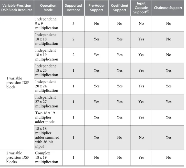
Table 3-1: Variable Precision DSP Blocks Operational Modes for Cyclone V Devices Variable-Precision
DSP Block Resource OperationMode SupportedInstance Pre-AdderSupport CoefficientSupport
Input Cascade
Support(1) Chainout Support
1 variable precision DSP block Independent 9 x 9 multiplication 3 No No No No Independent 18 x 18
multiplication 2 Yes Yes Yes No
Independent 18 x 19
multiplication 2 Yes Yes Yes No
Independent 18 x 25
multiplication 1 Yes Yes Yes Yes
Independent 20 x 24
multiplication 1 Yes Yes Yes Yes
Independent 27 x 27
multiplication 1 Yes Yes Yes Yes
Two 18 x 19 multiplier
adder mode 1 Yes Yes Yes Yes
18 x 18 multiplier adder summed with 36-bit input 1 Yes No No Yes 2 variable precision DSP blocks Complex 18 x 19 multiplication 1 No No Yes No
(1) When you enable the pre-adder feature, the input cascade support is not available.
Resources
Table 3-2: Number of Multipliers in Cyclone V Devices
The table lists the variable-precision DSP resources by bit precision for each Cyclone V device.
Variant MemberCode
Variable-precision DSP Block
Independent Input and Output
Multiplications Operator 18 x 18 Multiplier Adder Mode 18 x 18 Multiplier Adder Summed with 36 bit Input 9 x 9 Multiplier 18 x 18 Multiplier 27 x 27 Multiplier Cyclone V E A2 25 75 50 25 25 25 A4 66 198 132 66 66 66 A5 150 450 300 150 150 150 A7 156 468 312 156 156 156 A9 342 1,026 684 342 342 342 Cyclone V GX C3 57 171 114 57 57 57 C4 70 210 140 70 70 70 C5 150 450 300 150 150 150 C7 156 468 312 156 156 156 C9 342 1,026 684 342 342 342 Cyclone V GT D5 150 450 300 150 150 150 D7 156 468 312 156 156 156 D9 342 1,026 684 342 342 342 Cyclone V SE A2 36 108 72 36 36 36 A4 84 252 168 84 84 84 A5 87 261 174 87 87 87 A6 112 336 224 112 112 112 Cyclone V SX C2 36 108 72 36 36 36 C4 84 252 168 84 84 84 C5 87 261 174 87 87 87 CV-52003 2015.12.21 Resources 3-3
Design Considerations
You should consider the following elements in your design: • Operational modes
• Internal coefficient and pre-adder • Accumulator
• Chainout adder
Operational Modes
The Quartus Prime software includes IP cores that you can use to control the operation mode of the multipliers. After entering the parameter settings with the IP Catalog, the Quartus Prime software automatically configures the variable precision DSP block.
Altera provides two methods for implementing various modes of the Cyclone V variable precision DSP block in a design—using the Quartus Prime DSP IP cores and HDL inferring.
The following Quartus Prime IP cores are supported for the Cyclone V variable precision DSP blocks implementation: • LPM_MULT • ALTERA_MULT_ADD • ALTMULT_COMPLEX • ALTMEMMULT Related Information
• Introduction to Altera IP Cores
• Integer Arithmetic IP Cores User Guide
• Floating-Point IP Cores User Guide
• Quartus II Software Help
Internal Coefficient and Pre-Adder
To use the pre-adder feature, all input data and multipliers must have the same clock setting. The input cascade support is not available when you enable the pre-adder feature.
Accumulator
The accumulator in the Cyclone V devices supports double accumulation by enabling the 64-bit double accumulation registers located between the output register bank and the accumulator.
The double accumulation registers are set statically in the programming file.
Chainout Adder
You can use the output chaining path to add results from other DSP blocks.
Block Architecture
The Cyclone V variable precision DSP block consists of the following elements: • Input register bank
• Pre-adder
• Internal coefficient • Multipliers
• Adder
• Accumulator and chainout adder • Systolic registers
• Double accumulation register • Output register bank
If the variable precision DSP block is not configured in systolic FIR mode, both systolic registers are bypassed.
Figure 3-1: Variable Precision DSP Block Architecture for Cyclone V Devices
Input Regist er B ank scanin LOADCONST ACCUMULATE NEGATE dataa_y0[18..0] dataa_z0[17..0] dataa_x0[17..0] COEFSELA[2..0] datab_y1[18..0] datab_z1[17..0] datab_x1[17..0] COEFSELB[2..0] SUB_COMPLEX +/-Pre-Adder +/-Pre-Adder +/-Internal Coefficient Multiplier Adder +/- +/-Systolic Registers (1) Systolic Register (1) Chainout adder/ accumulator + Output Regist er B ank Constant Double Accumulation Register chainin[63..0] Result[73..0] Multiplier x x CLK[2..0] ENA[2..0] ACLR[1..0] CV-52003 2015.12.21 Block Architecture 3-5
Input Register Bank
The input register bank consists of data, dynamic control signals, and two sets of delay registers. All the registers in the DSP blocks are positive-edge triggered and cleared on power up. Each multiplier operand can feed an input register or a multiplier directly, bypassing the input registers.
The following variable precision DSP block signals control the input registers within the variable precision DSP block:
• CLK[2..0]
• ENA[2..0]
• ACLR[0]
In 18 x 19 mode, you can use the delay registers to balance the latency requirements when you use both the input cascade and chainout features.
Figure 3-2: Input Register of a Variable Precision DSP Block in 18 x 19 Mode for Cyclone V Devices
The figures show the data registers only. Registers for the control signals are not shown.
dataa_y0[18..0] dataa_z0[17..0] dataa_x0[17..0] datab_y1[18..0] Delay registers datab_z1[17..0] datab_x1[17..0] Delay registers scanin[18..0] scanout[18..0] CLK[2..0] ENA[2..0] ACLR[0] CV-52003
Figure 3-3: Input Register of a Variable Precision DSP Block in 27 x 27 Mode for Cyclone V Devices
The figures show the data registers only. Registers for the control signals are not shown.
dataa_y0[26..0] dataa_z0[25..0] dataa_x0[26..0] scanin[26..0] CLK[2..0] ENA[2..0] ACLR[0] scanout[26..0]
Pre-Adder
Cyclone V DevicesEach variable precision DSP block has two 19-bit pre-adders. You can configure these pre-adders in the following configurations:
• Two independent 19-bit pre-adders • One 27-bit pre-adder
The pre-adder supports both addition and subtraction in the following input configurations: • 18-bit (signed) addition or subtraction for 18 x 19 mode
• 17-bit (unsigned) addition or subtraction for 18 x 19 mode • 26-bit addition or subtraction for 27 x 27 mode
Internal Coefficient
The Cyclone V variable precision DSP block has the flexibility of selecting the multiplicand from either the dynamic input or the internal coefficient.
The internal coefficient can support up to eight constant coefficients for the multiplicands in 18-bit and 27-bit modes. When you enable the internal coefficient feature, COEFSELA/COEFSELB are used to control
the selection of the coefficient multiplexer.
Multipliers
A single variable precision DSP block can perform many multiplications in parallel, depending on the data width of the multiplier.
There are two multipliers per variable precision DSP block. You can configure these two multipliers in several operational modes
• One 27 x 27 multiplier
• Two 18 (signed)/(unsigned) x 19 (signed) multipliers • Three 9 x 9 multipliers
Related Information
Operational Mode Descriptions on page 3-11
Provides more information about the operational modes of the multipliers.
Adder
You can use the adder in various sizes, depending on the operational mode: • One 64-bit adder with the 64-bit accumulator
• Two 18 x 19 modes—the adder is divided into two 37-bit adders to produce the full 37-bit result of each independent 18 x 19 multiplication
• Three 9 x 9 modes—you can use the adder as three 18-bit adders to produce three 9 x 9 multiplication results independently
Accumulator and Chainout Adder
The Cyclone V variable precision DSP block supports a 64-bit accumulator and a 64-bit adder. The following signals can dynamically control the function of the accumulator:
• NEGATE
• LOADCONST
• ACCUMULATE
Table 3-3: Accumulator Functions and Dynamic Control Signals
This table lists the dynamic signals settings and description for each function. In this table, X denotes a "don't care" value.
Function Description NEGATE LOADCONST ACCUMULATE
Zeroing Disables theaccumulator. 0 0 0
Loads an initial value
CV-52003
Function Description NEGATE LOADCONST ACCUMULATE
Accumulation Adds the currentresult to the previous
accumulate result. 0 X 1
Decimation
This function takes the current result, converts it into two’s complement, and adds it to the previous result.
1 X 1
Systolic Registers
There are two systolic registers per variable precision DSP block. If the variable precision DSP block is not configured in systolic FIR mode, both systolic registers are bypassed.
The second set of systolic registers are used to delay the chainout output to the next variable precision DSP block.
You must clock all the systolic registers with the same clock source as the output register bank.
Double Accumulation Register
The double accumulation register is an extra register in the feedback path of the accumulator. Enabling the double accumulation register will cause an extra clock cycle delay in the feedback path of the accumulator.
This register has the same CLK, ENA, and ACLR settings as the output register bank.
By enabling this register, you can have two accumulator channels using the same number of variable precision DSP block.
Output Register Bank
The positive edge of the clock signal triggers the 64-bit bypassable output register bank and is cleared after power up.
The following variable precision DSP block signals control the output register per variable precision DSP block:
• CLK[2..0]
• ENA[2..0]
• ACLR[1]
Operational Mode Descriptions
This section describes how you can configure an Cyclone V variable precision DSP block to efficiently support the following operational modes:
• Independent Multiplier Mode
• Independent Complex Multiplier Mode • Multiplier Adder Sum Mode
• 18 x 18 Multiplication Summed with 36-Bit Input Mode • Systolic FIR Mode
Independent Multiplier Mode
In independent input and output multiplier mode, the variable precision DSP blocks perform individual multiplication operations for general purpose multipliers.
Table 3-4: Variable Precision DSP Block Independent Multiplier Mode Configurations
Configuration Multipliers per block
9 x 9 3 18 (signed) x 18 (unsigned) 2 18 (unsigned) x 18 (unsigned) 18 (signed) x 19 (signed) 18 (unsigned) x 19 (signed) 18 x 25 1 20 x 24 1 27 x 27 1 CV-52003
9 x 9 Independent Multiplier
Figure 3-4: Three 9 x 9 Independent Multiplier Mode per Variable Precision DSP Block for Cyclone V Devices
Three pairs of data are packed into the ax and ay ports; result contains three 18-bit products.
Input Regist er B ank Multiplier x Result[53..0] (p2, p1, p0) ay[y2, y1, y0]
ax[x2, x1, x0] 27 27 54 Variable-Precision DSP Block Output Regist er B ank
18 x 18 or 18 x 19 Independent Multiplier
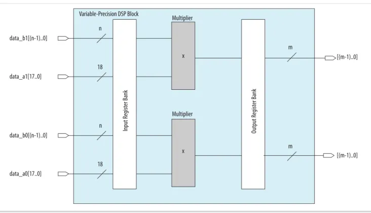
Figure 3-5: Two 18 x 18 or 18 x 19 Independent Multiplier Mode per Variable Precision DSP Block for Cyclone V Devices
In this figure, the variables are defined as follows: • n = 19 and m = 37 for 18 x 19 mode
• n = 18 and m = 36 for 18 x 18 mode
[(m-1)..0] Multiplier x Multiplier x Input Regist er B ank data_b1[(n-1)..0] data_a1[17..0] n 18 Variable-Precision DSP Block data_b0[(n-1)..0] data_a0[17..0] n 18 m [(m-1)..0] m Output Regist er B ank 3-12 9 x 9 Independent Multiplier 2015.12.21CV-52003
18 x 25 Independent Multiplier
Figure 3-6: One 18 x 25 Independent Multiplier Mode per Variable Precision DSP Block for Cyclone V Devices
In this mode, the result can be up to 52 bits when combined with a chainout adder or accumulator.
Input Regist er B ank Multiplier Result[42..0] dataa_b0[17..0] dataa_a0[24..0] 18 25 43 Variable-Precision DSP Block Output Regist er B ank x
20 x 24 Independent Multiplier
Figure 3-7: One 20 x 24 Independent Multiplier Mode per Variable Precision DSP Block for Cyclone V Devices
In this mode, the result can be up to 52 bits when combined with a chainout adder or accumulator.
Input Regist er B ank Multiplier x Result[43..0] dataa_b0[19..0] dataa_a0[23..0] 20 24 44 Variable-Precision DSP Block Output Regist er B ank CV-52003 2015.12.21 18 x 25 Independent Multiplier 3-13
27 x 27 Independent Multiplier
Figure 3-8: One 27 x 27 Independent Multiplier Mode per Variable Precision DSP Block for Cyclone V Devices
In this mode, the result can be up to 64 bits when combined with a chainout adder or accumulator.
Input Regist er B ank Multiplier x Result[53..0] dataa_b0[26..0] dataa_a0[26..0] 27 27 54 Variable-Precision DSP Block Output Regist er B ank
Independent Complex Multiplier Mode
Figure 3-9: Sample of Complex Multiplication Equation
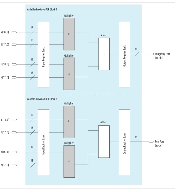
18 x 19 Complex Multiplier
Figure 3-10: One 18 x 19 Complex Multiplier with Two Variable Precision DSP Blocks for Cyclone V Devices Variable-Precision DSP Block 1 Variable-Precision DSP Block 2 Input Regist er B ank Imaginary Part (ad+bc) Multiplier c[18..0] b[17..0] 19 18 Multiplier d[18..0] a[17..0] 19 18 38 Adder + x x Output Regist er B ank Input Regist er B ank Real Part (ac-bd) d[18..0] b[17..0] 19 18 c[18..0] a[17..0] 19 18 38 Output Regist er B ank Multiplier Multiplier Adder -x x CV-52003 2015.12.21 18 x 19 Complex Multiplier 3-15
Multiplier Adder Sum Mode
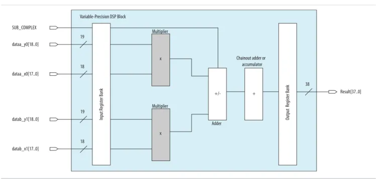
Figure 3-11: One Sum of Two 18 x 19 Multipliers with One Variable Precision DSP Block for Cyclone V Devices Input Regist er B ank Result[37..0] dataa_y0[18..0] dataa_x0[17..0] 19 18 Variable-Precision DSP Block datab_y1[18..0] datab_x1[17..0] 19 18 38 Multiplier Multiplier Adder +/-Chainout adder or accumulator SUB_COMPLEX Output Regist er B ank + x x
18 x 18 Multiplication Summed with 36-Bit Input Mode
Cyclone V variable precision DSP blocks support one 18 x 18 multiplication summed to a 36-bit input. Use the upper multiplier to provide the input for an 18 x 18 multiplication, while the bottom multiplier is bypassed.
Figure 3-12: One 18 x 18 Multiplication Summed with 36-Bit Input Mode for Cyclone V Devices
Input Regist er B ank Result[36..0] dataa_y0[17..0] dataa_x0[17..0] 18 18 Variable-Precision DSP Block datab_y1[35..18] datab_y1[17..0] 18 18 37 Multiplier Adder Chainout adder or accumulator SUB_COMPLEX Output Regist er B ank x +/- +
Systolic FIR Mode
The basic structure of a FIR filter consists of a series of multiplications followed by an addition.
Figure 3-13: Basic FIR Filter Equation
Depending on the number of taps and the input sizes, the delay through chaining a high number of adders can become quite large. To overcome the delay performance issue, the systolic form is used with additional delay elements placed per tap to increase the performance at the cost of increased latency.
Figure 3-14: Systolic FIR Filter Equivalent Circuit
x[n]
y[n]
C1 C2 Ck-1 Ck
Cyclone V variable precision DSP blocks support the following systolic FIR structures: • 18-bit
• 27-bit
In systolic FIR mode, the input of the multiplier can come from four different sets of sources: • Two dynamic inputs
• One dynamic input and one coefficient input • One coefficient input and one pre-adder output • One dynamic input and one pre-adder output
18-Bit Systolic FIR Mode
In 18-bit systolic FIR mode, the adders are configured as dual 44-bit adders, thereby giving 8 bits of overhead when using an 18-bit operation (36-bit products). This allows a total of 256 multiplier products.
CV-52003