Using Direct Solid Sampling ICP-MS to Complement
SEM-EDX and SIMS in Characterizing Semiconductor Materials
Fuhe Li
∗and Scott Anderson
†Air Liquide America-Balazs Analytical Services, 46409 Landing Parkway, Fremont, CA 94538
Abstract. The coupling of laser ablation systems with inductively coupled plasma (ICP) mass spectrometry has been
done for many years, however the quantitative aspects as well as the applications have often been limited. Recently, LA ICP-MS has been developed into a valuable analytical tool in our laboratory to address new applications, and some experimental difficulties encountered by SEM-EDX and SIMS in characterizing solid semiconductor, electronic, and optical communication materials. In this paper we will discuss many of the applications as well as the pros, cons, and complimentary features of the laser ablation technique as it relates to electronics industry issues.
Key Words. Laser ablation, ICP-MS, inductively coupled plasma, semiconductor material analysis, and solid analysis.
∗ Email: [email protected] † Email: [email protected]
INTRODUCTION
Laser ablation (LA) is by far the most versatile solid sampling technique for ICP mass spectrometry (ICP-MS) [1-3]. LA ICP-MS involves the conversion of solid materials into a plume of atomic vapor and micro particles by focusing a high-power and pulsed laser beam onto a sample surface. The plume of atomic vapor and micro particles is transported in an argon carrier gas to the steady-state RF plasma (ICP) for efficient atomization and ionization (Figure 1). The ions produced by the ICP are then analyzed by either a quadrupole or a magnetic sector based high-resolution mass spectrometer.
Figure 1. Conceptual diagram of LA ICP-MS
Unlike SIMS analysis, LA ICP-MS spatially and temporally separates its ionization from the sampling process (Figure 1). The laser in this arrangement is solely used for sampling. The steady state ICP plasma with typical electron temperature around 10,000 K [1] is used for ionization due to its constant high thermal energy and relative long sample-plasma interaction time. It is important to note that the sampling and ionization are two fundamentally different processes requiring very different optimization conditions [4]. The spatial and temporal separation of sampling and ionization enables separate operation and independent optimization resulting in much more efficient ionization and more quantitative measurements with less matrix effects.
With the availability of NIST traceable solid standards developed in our laboratory, we have used LA-ICP-MS for both qualitative and quantitative analyses of semiconductor and electronics materials. Examples of the materials analyzed to date include particles, silicon wafers, raw silicon materials, quartz, aluminum nitride, ceramic wafers, graphite, low-k fluoro polymer, copper interconnect, bonding wires, metal films, and silicon carbide (SiC). Both conductive and insulating materials can be analyzed in their natural states using LA ICP-MS without any sample pre-treatments such as Au coating or charge neutralization. Both compositional analysis and trace impurities determination have been performed with LA ICP-MS. ICP Sampling/Vaporization/Sputtering Atomization/Ionization Ar Carrier UV Laser Sample in LA Chamber M+ Ions
This paper focuses on the LA ICP-MS methodologies developed in our laboratory and their applications in characterizing semiconductor and electronics materials. The emphasis will be given to how LA ICP-MS complements SEM-EDX and SIMS in both qualitative and quantitative analyses. Several case studies along with sample analyses of “real-world” materials will be presented.
QUALITATIVE ANALYSIS
Manufacturing yield in the electronics industry is quite often impacted due to micro-contamination in the form of a residue, powder, particle, discoloration, stain, or simply an unknown material. Identification of these unknowns using LA ICP-MS in conjunction with SEM-EDX has been found to be more comprehensive and conclusive than just using SEM-EDX alone.
Particle Identification
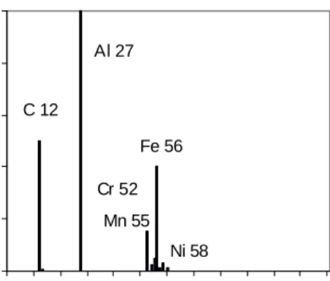
LA ICP-MS is at least 1000 times more sensitive than SEM-EDX when being used in identifying an unknown. It can analyze not only those elements lighter than Al such as B, Be, C, and Li but also the light elements in the presence of heavy elements. This latter task is not straight-forward with SEM-EDX as the energy lines of heavy elements often overlap with the energy lines of light elements. One example of using LA ICP-MS to confirm the presence or absence of the elements at or below the SEM-EDX detection limit levels is an analysis we have performed on a brownish powder sample collected in a stainless steel process line. SEM-EDX analysis was first conducted and the EDX spectrum showed only Al and O. However, Al2O3 could not explain the brown coloration of the powders. The sample powder was then analyzed by LA ICP-MS, which not only identified Al, but also Fe, Cr, Ni, Mn, Cu, and C (Figure 2). Based on the information provided by both SEM-EDX and LA ICP-MS, the engineers identified the brownish powder buildup as a mixture of Al processing chemical and rust from the stainless steel, and quickly found the contamination sources in the process line.
With no continuous background and a greater spectral resolution, LA ICP-MS can help identify the elements that typically have spectral overlaps in a SEM-EDX analysis [5]. An example of such a problem is presented below. A process engineer experiencing a black particulate contamination in a plating bath, analyzed the particles by SEM-EDX and observed an intense signal at ~ 4.5 KeV. Based on the EDX spectrum the analyst was unable to identify whether the contaminant was Ba or Ti because both show up at the
0 80000 160000 240000 320000 400000 0 20 40 60 80 100 120 m /z (amu) Signal Intensity (c/s) Al 27 C 12 Fe 56 Cr 52 Ni 58 Mn 55
Figure 2. Mass spectrum obtained from analysis of brownish powders collected from a stainless steel process line.
4.5 KeV energy level. The same sample was analyzed by LA ICP-MS where the m/z resolution (Ba at m/z 138 and Ti 48) was easily determined and the particles confirmed as Ba (Figure 3). Another example will be the analysis of a non-conductive material for P and S by SEM-EDX, where the required Au coating process makes the identification of P and S very difficult due to the overwhelming spectral overlaps. However, this is a rather easy analysis by LA ICP-MS.
0 70000 140000 210000 280000 350000 420000 20 60 100 140 180 m /z (amu) Signal Intensity (c/s) Ba 138 Ti 48
Figure 3. Mass spectrum obtained with analysis of black
particles collected from a plating bath. The analysis of mass-to-charge ratio via mass spectrometry gives unambiguous identification not possible with SEM-EDX.
Volatile contaminants can also be difficult to identify by SEM-EDX and other vacuum technologies such as SIMS. These techniques can lose the volatile analytes in the vacuum chamber when the electron or ion beam bombards the sample. Since the sampling stage of LA ICP-MS is operated at atmospheric pressure and there is no vacuum involved, volatile
contaminants are easily analyzed by LA ICP-MS. In fact, LA ICP-MS involves a transformation of a solid into vapor phase prior to the mass spectrometric measurement step. The analysis of a volatile sample by LA ICP-MS is rather easy compared to the analysis of a refractory material.
Film Consistency
Recently, the applicability of LA ICP-MS as a depth-profiling tool was studied for dielectric thin-films, copper interconnects, and many thick films used in optical communication fields. Although the depth resolutions obtained with LA ICP-MS (0.05-0.1µm depending on the materials) were moderate compared to SIMS, its simultaneous multi-element depth-profiling capability has shown great applicability to some problems encountered in ULSI technology processes, especially in monitoring the consistency of major constituents in metal films.
Figure 4 shows a depth profile of a 1-µm Cu thin film obtained by LA ICP-MS without applying any smoothing. The Cu thin film contains a major metal additive in its bulk and was deposited on a Ta/TaN barrier layer. Because the LA ICP-MS was optimized for all elements of interest, the depth profiles for all elements were simultaneously obtained at one analysis spot under the same operating conditions. A qualitative screening for trace impurities in the film can
1.E+01 1.E+02 1.E+03 1.E+04 1.E+05 1.E+06 -0.20 0.00 0.20 0.40 0.60 0.80 Estimated Depth (µm) Signal Intensity (c/s) Cu Metal Additive Ta/TaN
Figure 4. Depth profile of a 1 µm copper thin film
also be performed. Since non-uniformity does occur in some films, the authors believe that the depth profile obtained by simultaneous multi-element measurement at a single spot is more representative than overlapping the depth profiles obtained from separate analyses, especially those done at different sampling spots using
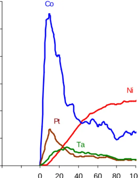
more than one ionization source under various instrumental conditions. Another example of this type of application is shown in Figure 5. Here, a penetration depth of approximately 100 nm was used to generate a depth profile of a hard disk drive.
0 4000 8000 12000 16000 20000 24000 -40 -20 0 20 40 60 80 100 Estimated Depth (nm ) Relative Intensity Co Ni Pt Ta
Figure 5. Depth profile for the top layer of a hard disk drive
Spatial Mapping
LA ICP-MS was also used to study both vertical and horizontal diffusion of a refill material deposited via focused ion beam (FIB) in bulk silicon. Although it is beneficial to use a FIB to refill some pits left on a wafer, the refill material that contains high percentages of dopant such as Ga can become a source of contamination, especially during a high-temperature annealing step [6]. The worse case showed that the Ga spreading could be as large as 1 cm from the center of the refilled material on a wafer. We have used LA-ICP-MS to measure the vertical and lateral distributions of Ga around a FIB cut to help the process engineers to better understand and control the diffusion.
QUANTITATATIVE ANALYSIS
ICP-MS has long been the dominant quantitative tool for trace elemental analysis of liquid samples. This is due to its superior overall performance in terms of detection limits, sensitivity, analytical precision and accuracy, less spectral interference, elemental coverage, and a linear calibration range that is nearly eight orders of
magnitude [7]. By coupling ICP-MS with Laser Ablation, direct solids analysis for trace metals without going through the chemical dissolution step is possible. Because it spatially and temporally separates sampling and ionization steps in an analysis, the optimized LA-ICP-MS is able to produce more quantitative and representative ion counts for trace elements in a given matrix.
Trace Metals
Analysis
Trace metallic impurities present in the bulk materials used in IC manufacturing have been found to affect the performance, integrity, and the lifetime of a device. Quantitative analysis of these impurities and tight control of incoming materials are essential. With the availability of NIST traceable solid standards in our laboratory, we have been able to construct linear calibration curves for all elements of interest. Our initial work for quantitative analysis of trace impurities in a solid was done by coupling the LA system with the least sensitive ICP-MS in our laboratory. The initial detection limits obtained in terms of absolute mass (ng) for quantitative analysis of 40 trace elements in bulk silicon are listed in Table 1.
Table 1. Initial detection limits obtained using LA-ICP-MS for quantitative analysis of trace impurities in bulk silicon.
Element DLs Element DLs (ng) (ng) Ag 0.2 La 0.001 Al 0.05 Li 0.7 As 0.02 Mg 0.1 Au 0.06 Mn 0.01 B 0.2 Mo 0.01 Ba 0.001 Na 0.4 Be 0.05 Ni 0.2 Bi 0.001 P 0.3 Ca 2 Pb 0.02 Cd 0.02 Sb 0.003 Ce 0.001 Sc 0.05 Co 0.01 Sn 0.01 Cr 0.03 Sr 0.002 Cu 0.1 Ta 0.0004 Fe 0.2 Ti 0.1 Ga 0.02 Tl 0.001 Ge 0.02 V 0.004 Hg 0.2 W 0.002 In 0.0004 Zn 0.04 K 0.3 Zr 0.001
Note that the detection limits could be improved by as many as two orders of magnitude when coupling the LA system with a more sensitive ICP-MS. Additionally increasing analysis time by sampling more material using the laser can also be used as a strategy to further lower the detection limits. Finally, LA ICP-MS can perform a so-called layer-by-layer analysis, for example at 1 µm increment, for trace impurities. This particular analysis scheme seems to be useful in locating the trace impurities in a bulk material and studying their vertical profiles.
Total Dose Measurement
The total dopant dose implanted in crystalline silicon is currently estimated using sheet resistance, capacitance-voltage (C-V), thermal wave, and SIMS techniques [8-9]. Due to their indirect measurement nature, the analyses by sheet resistance, capacitance-voltage (C-V), and thermal wave are often affected by the presence of other ions in crystalline silicon and different annealing conditions. SIMS is an excellent depth profiler. However, establishing the accuracy of total dose measurement is difficult.
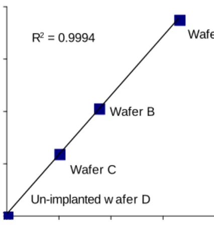
LA ICP-MS has been studied in our laboratory for quantitative analysis of total dopant dose to help monitor and control the ion implantation process. It is our hope that this method can eventually be utilized to calibrate ion implanters in different fabrications and to correlate the total dose levels used in different IC processes. Four commonly used dopant ions, namely 11B+, 75As+, 121Sb+, and 31P+, were investigated. Their dynamic calibration ranges, accuracy and precision, short-term and long-term repeatability by LA-ICP-MS were studied. Figure 6 shows the calibration curve for
R2 = 0.9994 0 200000 400000 600000 800000
0.E+00 2.E+15 4.E+15 6.E+15 8.E+15 As Surface Concentration (atom s /cm 2)
Integrated Intensity
Wafer A
Wafer B
Wafer C Un-implanted w afer D
the quantitative analysis of 75As+ implant with LA ICP-MS. The curve was constructed using different wafers with known dose levels implanted under various implantation conditions. These wafers also have different crystal orientations and were either annealed or un-annealed. As shown in Figure 6, the curve shows an acceptable linearity, which was not affected by the matrix orientation differences or whether the wafers were annealed. Similar curves were also obtained for 11B+, 121Sb+, and 31P+. No obvious competitive and suppressive processes were observed for LA ICP-MS. No surface charging was found in LA ICP-MS. These processes are usually the factors that can hinder the dynamic ranges of SIMS and make SIMS quantitative analysis more problematic to achieve.
Multiple silicon wafers implanted with a constant dose level were used to assess the analytical precision and accuracy of LA ICP-MS for total dose measurement. The initial quantitative results obtained for 11B+ and 75As+ are shown in Table 2. The predicted values were estimated either by four-point probe or SIMS. It can be seen that the ICP-MS results were in the predicted dose ranges. We are currently continuing our efforts to improve the analytical precision by modifying the method and optimizing both laser and ICP-MS operating parameters.
Table 2. Quantitative analysis of total 11B+, 75As+ doses implanted in silicon.
Ion Predicted Found S.D. RSD (Ions/cm2) (Ions/cm2) (Ions/cm2) %
11
B+ 5E14 6.6E14 0.3E14 4.5 11
B+ 2E15 2.1E15 0.2E15 9.5 75As+ 4E15 3.5E15 0.2E15 5.7 75
As+ 7E15 6.6E15 0.2E15 3.0
Microscopic Analysis
By properly tuning the laser parameters and utilizing the matrix-matched standards, we have been able to use LA ICP-MS to quantitatively analyze some microscopic features for elemental compositions. In this analysis mode, the laser is focused on one spot, and a single pulse or brief burst of pulses is applied. Laser spot sizes as small as 5 µm are possible providing good spatial resolution. Examples of the materials analyzed by LA ICP-MS range from the inclusions on the quartz used as the inner wall coating for a CVD chamber to the PbSn solder bumps (~100 µm in diameter) on a finished chip used for bonding/packaging. Quantitative results obtained for
PbSn bumps were confirmed and verified using wet chemical analysis.
CONCLUSIONS
Although laser ablation has been researched in conjunction with ICP-MS for close to twenty years, difficulties with sample transport and proper standards have often limited overall analysis utility. Work in this laboratory has addressed many of these issues and applications for both qualitative and quantitative analyses have been applied to electronics industry problems. LA ICP-MS has been shown to be both a complementary and supplementary technique to SIMS and SEM-EDX analyses. In the end, customers can achieve a more complete answer for fab related problems.
REFERENCES
1. Montaser, A., Minnich, M.G., McLean, J.A., and Liu, H., “Sample Introduction in ICP-MS,” in Inductively
Coupled Plasma Mass Spectrometry, edited by A.
Montaser, Wiley-VCH, New York, 1998, pp. 83-264. 2. Russo, R.E., Appl. Spectrosc.,49, 14A-28A (1995). 3. Russo, R.E., Mao, X., Mao, S., G.M., Anal. Chem. 74,
70A-77A (2002).
4. Borer, M.W., Hiefjue, G.M., Spectrochim. Acta Review,
14, 463-486 (1991).
5. Goldstein, J.I., Newbury, D.E., Echlin, P., Joy, D.C., Romig, A.D., Lyman, C.E., Fiori, C., and Lifshin, E.,
Scanning Electron Microscopy and X-Ray Microanalysis,
Plenum Press, New York, 1994, pp. 365-393.
6. Weiland, R., Tittes, W., and Jackman, J., The Proceedings of 26th International Symposium for Testing and Failure Analysis, Bellevue, WA, 2000. Also published in Micro, Defect/Yield Analysis, (2001).
7. Montaser, A., Minnich, M.G., McLean, J.A., and Liu, H., “Sample Introduction in ICP-MS,” in Inductively
Coupled Plasma Mass Spectrometry, edited by A.
Montaser, Wiley-VCH, New York, 1998, pp. 1-31. 8. Current, M.I. Current, Basics of Ion Implantation for
Integrated Circuit Manufacturing, Greater Silicon Valley
Ion Implant Users Group, ch. 3, pp. 1-10, 1994.
9. Li, F., Balazs, M.K., and Pong, R., J. Anal. At. Spectrm.,