The Impact of Data Transfer and Buffering Alternatives on Network Interface Design
Shubhendu S. Mukherjee and Mark D. Hill
Computer Sciences DepartmentUniversity of Wisconsin-Madison 1210 W. Dayton Street Madison, Wisconsin 53706-1685, USA
{shubu,markhill}@cs.wisc.edu
To appear in the Proceedings of the Fourth International Symposium on High-Performance Computer Architecture (HPCA), February 1998
Abstract
The explosive growth in the performance of microprocessors and networks has created a new opportunity to reduce the latency of fine-grain communication. Microprocessor clock speeds are now approaching the gigahertz range. Network switch latencies have dropped to tens of nanoseconds. Unfortunately, this explo-sive growth also exposes processor accesses to the network inter-face (NI) as a critical bottleneck for fine-grain communication. Researchers have proposed several techniques, such as using block loads and stores, User-Level DMA, and Coherent Network Interfaces, to alleviate this NI access bottleneck.
This paper is the first to systematically identify, examine, and evaluate the key parameters that underlie these design alterna-tives. We classify these parameters into two categories: data transfer and buffering parameters. The data transfer parameters capture how messages are transferred between internal memory structures (e.g. processor caches, main memory) of a computer and a memory bus NI. The buffering parameters capture how and where an NI buffers incoming network messages.
We evaluate seven memory bus NIs that we believe capture the essential components of the design space exposed by these data transfer and buffering parameters. These seven NIs abstract the data transfer and buffering parameters of the NIs in TMC CM-5 [24], Fujitsu AP3000 [37], Princeton User-Level DMA [2], Digi-tal Memory Channel [16], MIT StarT-JR [20], and two Coherent Network Interfaces (CNI512Q and CNI32Qm) [29].
Our results indicate that a high-performance NI design should effectively use the block transfer mechanism of the memory bus, minimize processor involvement for data transfer, directly transfer messages between an NI and the processor (at least in the com-mon case), provide plentiful buffering (possibly in main memory), and minimize processor involvement to buffer incoming network messages. The relative importance of these parameters depends both on the specific NI design and the characteristics of the appli-cation.
As a corollary of this study, we find that, contrary to conven-tional wisdom, mapping an NI to the processor registers is usually not the ideal choice. This is because processor register memory is a precious resource, which does not provide adequate buffering for many applications.
1 Introduction
The term “computer” is perhaps a misnomer today. A modern computer system often “communicates” with a communication network more than it “computes.” A network interface (NI) device provides a computer with a gateway to such external networks.
Unfortunately, processor accesses to an NI threaten to become a critical bottleneck in computers today. This is because of two reasons. First, the explosive growth in microprocessor and net-work performance has vastly increased the rate at which proces-sors communicate with external networks. Microprocesproces-sors continue to evolve with gigahertz clocks and increasing levels of instruction-level parallelism. Network hardware continues to advance towards multi-gigabytes-per-second bandwidth and
tens-of-nanoseconds switch latencies. Consequently, rapid processor access to the NI is critical to effectively use such extremely fast microprocessor and network hardware.
Second, processor accesses to an NI form an important compo-nent of end-to-end latency for fine-grain communication. Fine-grain communication underlies many traditional and emerging application domains, such as parallel scientific applications [10], network file systems [22], world-wide web servers [1], and data-base queries [23]. A major fraction of messages in these domains are small messages that are less than a few kilobytes.
Traditional NIs reside on the I/O bus and are accessed via either uncached loads/stores or Direct Memory Access (DMA). However, such traditional solutions cannot alleviate the NI access bottleneck. Today’s I/O buses offer latencies and bandwidth that are a factor of two to ten worse than memory buses. Consequently, several commercial NI designers and researchers have proposed moving the NI from the I/O bus to the memory bus. For example, parallel computers, such as the TMC CM-5 [41], Meiko CS2 [28], and Intel Teraflops [6] attach their NIs directly to the memory bus.1
Both uncached accesses and DMA are low-performance solu-tions to accessing an NI device residing on the memory bus. Tra-ditionally, uncached accesses transferred only between one to eight bytes of data, which cannot effectively use today’s 16- to 32-byte wide memory buses (e.g. Sun UltraGigaplane). On the other hand, traditional DMA usually requires the operating system to perform many tasks to initiate a transfer between memory and an I/O device. Consequently, the overhead to initiate a DMA transfer can be as high as hundreds or thousands of instructions. This makes traditional DMA highly inefficient for small data transfers that underlie fine-grain communication.
Fortunately, today there exists a range of innovative solutions that have the potential to alleviate this NI access bottleneck. For example, the Sun UltraSparc processor [39] offers new user-level block load and store instructions. These block loads and stores can move 64-byte blocks of data between an I/O device and the float-ing-point registers. The Fujitsu AP3000 [38] parallel computer uses these UltraSparc block load/store instructions to access its NI. Blumrich, et al. [2] proposed a new mechanism called User-Level DMA (UDMA) that dramatically reduces the DMA initia-tion overhead to just two user-level instrucinitia-tions. Alternatively, Mukherjee, et al. [29] proposed a new class of NIs called Coher-ent Network Interfaces (CNIs) that interface directly to the mem-ory bus’ coherence protocol. This allows data transfer between a processor cache and a CNI in whole cache block units and
plenti-1. Attaching the NI to the memory bus may require a non-standard inter-face, which may prevent third-party vendors from manufacturing NIs. Mukherjee and Hill [30, 31] discuss several solutions to this problem. This work is supported in part by Wright Laboratory Avionics Directorate, Air Force Material Command, USAF, under grant #F33615-94-1-1525 and ARPA order no. B550, National Science Foundation with grants MIP-9225097, MIPS-9625558, and CDA-9623632, a Wisconsin Romnes Fellowship, and donations from Sun Microsystems. The U.S. Government is authorized to reproduce and distribute reprints for Governmental purposes notwithstanding any copyright nota-tion thereon. The views and conclusions contained herein are those of the authors and should not be interpreted as necessarily representing the official policies or endorsements, either expressed or implied, of the Wright Laboratory Avionics Directorate or the U.S. Government.
ful buffering in main memory.
In this paper we systematically identify, examine, and evaluate the key parameters that underlie these design alternatives. A thor-ough understanding of these key parameters is critical to designing high-performance NIs.
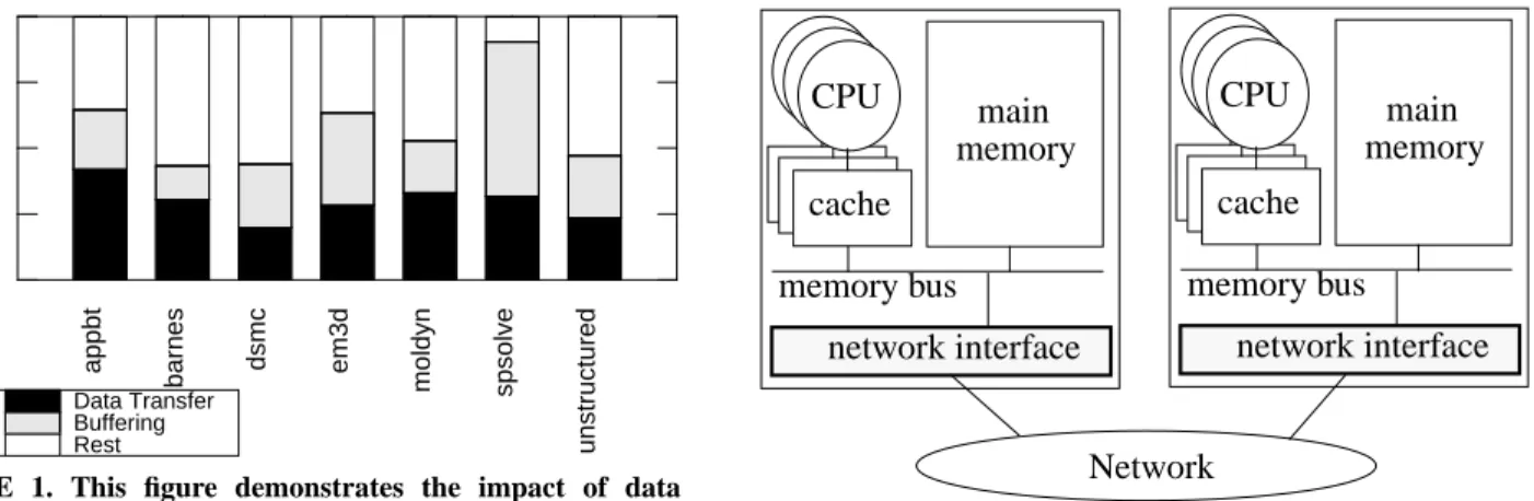
We classify these key parameters into two categories: data trans-fer and buftrans-fering parameters. The data transtrans-fer parameters capture how messages are transferred between a processor and an NI. The buffering parameters capture where and how an NI buffers incom-ing network messages. Figure 1 shows the impact of data transfer and buffering parameters on the performance of seven parallel sci-entific applications studied in this paper. This figure shows that data transfer and buffering can respectively account for upto 42% and 58% of the total execution time of these parallel programs. In other words, proper choices of the data transfer and buffering parameters can have a dramatic impact on performance.
The data transfer and buffering parameters expose an enormous NI design space. This is because these parameters can be imple-mented in several different ways. In this paper we evaluate seven memory bus NIs that we believe capture the essential components of this design space. These seven memory bus NIs abstract the key data transfer and buffering parameters of the NIs for the TMC CM-5 [24], Fujitsu AP3000 [38], Princeton User-Level DMA [2], Digi-tal Memory Channel [16], MIT StarT-JR [20], and two CNIs (CNI512Q and CNI32Qm) [29].
We evaluate these NIs using two microbenchmarks and seven macrobenchmarks. Our results indicate that a high-performance NI design must:
•
effectively use the block transfer mechanism of current memory buses,•
minimize processor involvement for data transfer,•
directly transfer messages between an NI and the processor, at least in the common case,•
provide plentiful buffering, possibly in main memory, and•
minimize processor involvement to buffer incoming network mes-sages.The relative importance of these parameters depends on both the specific NI design and the characteristics of the application.
These observations are, however, applicable primarily to
user-level NIs [31] targeted for fine-grain communication. NIs that require operating system intervention for message send and receipt or must transfer multi-megabytes of data directly from a graphics device or a disk (e.g. in a video server) may require optimizations that are different from those discussed in this paper.
We have two main contributions in this paper. First, we identify and examine the key data transfer and buffering parameters that underlie high-performance, user-level NI designs for fine-grain communication. Second, we undertake the first systematic simula-tion study that compares seven NIs representative of the design space exposed by these parameters. As a corollary of this study, we find that, contrary to conventional wisdom, mapping an NI to the processor registers may not be the ideal choice. This is because cessor register memory is a precious resource, which may not pro-vide adequate buffering for some applications.
The rest of the paper is organized as follows. Section 2 and Section 3 discuss the different data transfer and buffering parame-ters. Section 4 describes the seven memory bus NIs we studied in this paper. Section 5 describes our evaluation methodology. Section 6 discusses our results. Section 7 describes related work. Finally, Section 8 presents our conclusions.
2 Data Transfer Parameters
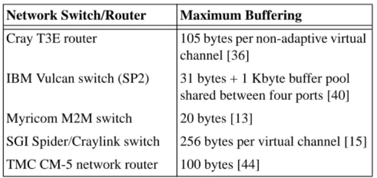
An NI is a device that sends and receives messages to and from an external network on behalf of the processor. Consequently, the most important data sent and received by an NI are network mes-sages. For high performance, NIs must transfer these messages rap-idly between the internal memory structures (e.g. processor registers, main memory) of a node and the NI. For memory bus NIs (Figure 2), such data transfer occurs over the memory bus.
We have identified and will discuss three key parameters that influence the speed of such data transfer:
•
size of transfer•
degree of processor involvement for transfer, and•
source and destination of transfer.2.1 Size of Transfer
Today most high-performance memory buses allow at least two data transfer sizes: small chunks (between one to eight bytes) and medium-sized blocks (between 16-64 bytes). The latter is more effi-cient than the former mechanism because block transfers can effec-tively use the bandwidth available from wide memory buses and amortize control overheads, such as bus arbitration, grant, and turn-appbt barnes dsmc em3d
moldyn spsolve unstructured 0 25 50 75 100 % Time Data Transfer Buffering Rest
FIGURE 1. This figure demonstrates the impact of data transfer and buffering on the performance of a memory bus NI for seven parallel scientific applications. For these measurements, we use a CM-5-like network interface and number of flow control buffers equal to 1. See Section 4 and Section 5 for a description of our CM-5-like NI, our flow control scheme, and the applications.
cache
main
memory
memory bus
network interface
CPU
cache
main
memory
memory bus
network interface
CPU
Network
FIGURE 2. This figure shows two workstation-like nodes connected via a network. The network interface attaches directly to the memory bus.
around time.
Several recent studies show that applications can effectively use such block transfers over the memory bus. Clearly, if the typical message size in fine-grain communication were a few bytes, block transfers over the memory bus would be useless. However, Cypher, et al. [10] found that in seven parallel scientific applications 30% of the messages were between 16 bytes and a kilobyte. Kay and Pas-quale [22] found that the median message sizes for TCP and UDP (mostly generated by the Network File System) traffic in a depart-mental network were 32 and 128 bytes respectively. They also found that 99% of TCP and 86% of the UDP traffic was less than 200 bytes. Keeton, et al. [23] analyzed a debitcredit benchmark on a commercial database and found that all messages were less than 200 bytes. In the seven parallel scientific applications we studied in this paper, we found that the average message size ranges between 19-230 bytes (Table 4 in Section 5).
Current microprocessors offer three mechanisms to effectively use the block transfer mechanism of memory buses. These are coa-lescing load/store buffers, block loads/stores, and cache blocks. A coalescing load/store buffer coalesces a processor’s accesses to consecutive addresses (and, in some cases, the same address) and transfers them as a single block over the memory bus. Therefore, a processor’s accesses to NI registers can be coalesced in the coalesc-ing buffers and transferred as a scoalesc-ingle block.
Block load/store instructions—recently introduced in the Sun UltraSparc processor [39]—allows a processor to move a block of data between a device, such as main memory or NI, and the UltraS-parc floating point registers. The Fujitsu AP3000 machine uses UltraSparc block load and store instructions to access the memory on the NI [37].
Finally, block transfer over the memory bus can be achieved by transferring data as cache blocks. However, this requires the NI to interact with the cache coherence signals, which are supported by most high-performance memory buses today. This is necessary to avoid having stale data in the processor’s cache. Currently, most DMA-based NIs transfer data in coherent, cache block units over the memory bus to avoid this problem. Recently, Mukherjee, et al. [29] developed techniques using which processors and NIs can communicate more effectively via coherent, cache block transfers.
2.2 Degree of Processor Involvement for Transfer
Performance of data transfer depends not only on the size of the transfer, but also on how much the processor is involved in the transfer. Two design alternatives exist. The processor can initiate the transfer and allow the NI to manage the rest of the transfer. Alternatively, the processor itself can actively manage the transfer.1 Each of these options have different design and performance impli-cations. We discuss these options below.
2.2.1 NI manages transfer
If the NI manages the transfer, then the processor is usually required to only initiate the data transfer between the NI and the internal memory structures of a node. Currently, a processor can use one of three mechanisms to initiate rapid data transfer to or from an NI: uncached load/store, User-Level DMA (UDMA), and cached store. An uncached load or store from the processor to a memory-mapped NI register can rapidly initiate data transfer from user space. However, an NI also needs physical memory addresses of data buffers from which it can obtain the data that must be
trans-1. A third option is possible in which a separate device or DMA engine manages the data transfer. We do not consider this option here.
ferred. Unfortunately, users cannot provide authenticated physical addresses of data buffers without violating most operating systems’ protection model. Consequently, NIs must be prepared to fetch authentic physical addresses from the operating system [35, 17, 42]. To avoid the complexity of building an NI that fetches and man-ages authentic physical addresses, Blumrich, et al. [2, 31] proposed a low-overhead data transfer initiation scheme called User-Level DMA (UDMA). In this scheme users provide authentic physical addresses to the NI via a sequence of two user-level instructions: an uncached store and an uncached load. Additionally, UDMA allows users to directly deposit data into user data structures.
Unfortunately, a key limitation of UDMA is that there is no known technique to extend UDMA in a general way to a multipro-grammed symmetric multiprocessing (SMP) node. The UDMA mechanism requires the two-instruction sequence to be atomic. However, in an SMP node, multiple such store-load sequences issued by multiple processors simultaneously can be overlapped leading to erroneous results. Markatos and Katevenis [26] showed the UDMA initiation sequence can be made atomic, but only under restricted conditions.
The multiprogramming problem faced by UDMA can be over-come using the third scheme in which processors and NIs commu-nicate via cachable, shared memory. To send a message a processor simply writes to a location shared between the processor and the NI (e.g. increment the shared tail pointer of a shared queue). The NI polls the shared location to determine the presence of a message. Similarly, when a message arrives at the NI, the NI sets a shared location that the processor monitors. This scheme does not face the same multiprogramming problem of UDMA. This is because such an NI can directly read and write data to a portion of the user’s address space, which is protected by the normal virtual memory mechanisms. However, like the first mechanism, this scheme does require the NI to fetch and manage authentic physical addresses to which the shared locations are mapped. Another drawback of this approach is that the NI must remember to poll the cached, shared locations to check for new messages. This is because, unlike uncached accesses, cached accesses by the processor is usually not visible outside the processor cache.
Cached stores additionally allow speculative processors to gen-erate messages speculatively [30]. A processor’s speculative stores are usually buffered locally inside the processor and committed only when the speculation succeeds. Consequently, a processor can speculatively issue a store to the cachable memory location shared between the processor and the NI. The store will, however, be visi-ble (and the message committed) to the processor only after the speculation succeeds and commits.
2.2.2 Processor manages transfer
The previous subsection discusses solutions in which the pro-cessor initiates and the NI manages the data transfer. An alternative solution is to allow the processor to both initiate and manage the data transfer. For example, traditional program-controlled I/O requires direct processor involvement to transfer data between the processor and the NI. In this scheme a processor directly reads and writes data (instead of addresses) to memory-mapped NI registers via uncached loads and stores. Even the Ultrasparc block load and store instructions require processor involvement because these instructions block the processor until the data transfer is complete.
Processor-managed transfers usually simplify the NI design because an NI does not require authentic physical addresses to access a message. A processor’s involvement for every data trans-fer, however, uses up precious processor resources, which can be used for other purposes (e.g. computation). Both UDMA and cache block transfers avoid processor involvement for data transfer, which
reduces processor occupancy and allows overlap of computation with data transfer.
2.3 Source and Destination of Transfer
For both message send and reception data must be transferred between source and destination memories located in the processor, NI, or main memory. The source and destination of data transfer impact performance in two ways: determining what technology is used for the source and destination memories and whether or not data travels from the source to the destination directly.
Memory technology influences performance because the perfor-mance of current memories vary widely. DRAMs—the dominant technology used for main memory—is usually much slower than SRAMs, which are used to build processor memories, such as regis-ters and caches. Consequently, transferring messages between the processor and NI via main memory, and not directly between the NI and processor, can hurt performance. Additionally, transferring messages between the processor and NI via main memory adds an extra hop over the memory bus, which adds extra latency. Neverthe-less, if the NI memory overflows, it may be more useful to buffer messages in main memory rather than blocking the network or dropping the message. We discuss these issues in the next section.
3 Buffering Parameters
The amount of buffering available for an NI can have significant impact on an NI’s performance. NIs can require large amounts of buffering because of four reasons. First, variation in performance of loosely-coupled microprocessors and network switches and advent of a variety user-level communication protocols often create a tem-porary mismatch between the rates at which network messages are generated, transferred, and consumed. Buffering smooths out these rates and helps create a balanced system.
Second, limited buffering often forces a processor to constantly monitor NI status changes and remove messages from the NI buff-ers to avoid clogging up the network. This constant monitoring can prevent the processor from doing useful computation.
Third, a limited amount of buffering severely restricts the degree of multiprogramming because these NI buffers must be divided among different processes. Alternatively, the operating system can switch the buffers among processes; but, this can be a very expen-sive operation.
Fourth, unreliable networks, such as the Myricom Myrinet, requires NIs to perform some form of flow-control, such as all-to-all buffer reservation or return-to-sender, to guarantee end-to-end reliable message delivery. To avoid clogging the network, such flow control schemes may require large amounts of buffering.
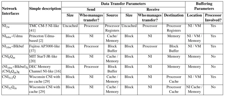
Unfortunately, NIs cannot rely on network switches/routers to provide this level of buffering. Current commercial network
switches/routers usually provide only a few hundred bytes of buff-ering (Table 1), which is usually sufficient to maintain the full bandwidth through the switch/router. However, if the receiving NI fails to remove messages from the network, the switches will block and send backpressure to the sender, thereby clogging up the net-work. Alternatively, switches, such as the Myricom Myrinet, sim-ply drop messages if the receiving NI fails to eject the message from the network. For such networks either the NI must have suffi-cient buffering to rapidly remove messages from the network or software must guarantee reliable delivery, which incurs substantial overhead.
The rest of this section discusses two parameters that influence the amount of buffering available to an NI: where the NI buffers are located (Section 3.1) and how much the processor is involved to buffer messages. (Section 3.2).
3.1 Location of NI Buffers
The location of NI buffers is influenced by two goals that may often be conflicting. We want NI buffers to be located such that the processor can access them rapidly. However, we also want the NI buffers to be plentiful.
Allocating NI buffers in the NI itself allows direct and rapid data transfer between the NI and processor. Unfortunately, supporting large amounts of dedicated memory on the NI to buffer messages may not be economically feasible. In contrast, main memory can support large amounts of buffering, but may not allow rapid data transfers (Section 2.3). Traditionally, NIs have either allocated mes-sage buffers in dedicated NI memory, main memory, or a hybrid combination of the two. We discuss the implications of hybrid designs in the next subsection.
One compromise that allows the best of both is to distinguish between the logical and physical location of NI buffers. Logically, we can allocate the message buffers in coherent, shared memory, which is plentiful. Physically, however, such NI buffers can be located in processor caches, main memory, or NI memory. A host node’s coherence protocol ensures that the different physical copies of the same (logical) message buffers are consistent across the node. In such a design, the NI memory behaves like another proces-sor cache in an SMP node. Thus, in the common case, the procesproces-sor can transfer data directly from the NI memory to the processor cache. However, if the NI memory overflows, the messages will be automatically replaced from NI memory to main memory, which allows plentiful buffering.
3.2 Degree of Processor Involvement for Buffering
If NI buffers are allocated both in dedicated NI memory and main memory, then either the processor or the NI must transfer messages from the dedicated NI memory to main memory. In the absence of such transfers, the network can fill up slowing down the entire system. More critically, in some situations, this can cause the system to deadlock. This is because the unavailability of message buffers can cause a cyclic dependence in which multiple processors are blocked (e.g. on a message send) waiting for other blocked pro-cessors to process incoming messages [24].Transfer of messages from dedicated buffers to main memory can be managed by either the processor or the NI. Who (processor or NI) manages such transfers depends on how often such buffering is required. For NIs that always store message data to a node’s main memory, processor involvement for buffering can seriously degrade performance. In contrast, NIs that are designed with the assumption that network “traffic jams” are rare occurrences may use processor-managed buffering as a fallback mechanism.
Network Switch/Router Maximum Buffering
Cray T3E router 105 bytes per non-adaptive virtual channel [36]
IBM Vulcan switch (SP2) 31 bytes + 1 Kbyte buffer pool shared between four ports [40] Myricom M2M switch 20 bytes [13]
SGI Spider/Craylink switch 256 bytes per virtual channel [15] TMC CM-5 network router 100 bytes [44]
TABLE 1. This table shows the amount of buffering available between an input port and an output port in five commercial network switches/routers.
4 Network Interface Implementations
This section describes the seven NIs we evaluate in this paper. Given the enormity of the design space exposed in Section 2 and Section 3, it would be hard to evaluate each and every component individually. Hence, we have selected seven NIs that, we believe, capture the essential components of the data transfer and buffering parameters. For all of our NIs, we assume a uniform network and flow control mechanism described in Section 5.
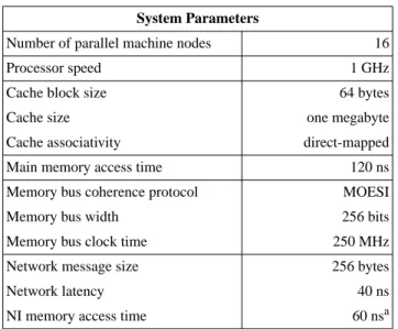
We use the Mukherjee, et al. [29] classification of NIs to character-ize the NIs we study in this paper. In this classification NIiX denotes traditional fifo-based NIs and CNIiX denotes coherent net-work interfaces. Processors interact with CNIiXs with coherent, cache block transfers. The subscript i denotes the size of the NI queue exposed to the processor. The default unit of i is memory/ cache blocks, but can also be specified in 4-byte words by adding the suffix ‘w’. The placeholder X could either be empty, Q, or Qm. X empty represents the simple case where a NI exposes only part or whole of one network message. X = Q represents the more complex case where the exposed portion of the NI queue is managed as a memory queue with explicit head and tail pointers. X = Qm denotes that the home of the explicit memory-based NI queues are in main memory. The home of a physical address is the I/O device or mem-ory module that services requests to that address (when the address is not cached) and accepts the data on writebacks (e.g. due to cache replacements). The absence of ‘m’ implies that the NI serves as the home for the NI queues. All of our CNI implementations use the three optimizations—lazy pointer, message valid bit, and sense reverse—described in [29].
Table 2 lists the seven NIs we evaluate in this paper. Column two of this table gives a simple description of these NIs to aid read-ers in remembering which NI is which. We will use both descrip-tions (column one and two) interchangeably in the rest of the paper.
NI2w is a CM-5-like NI in which the processor can access only the first two words of the NI fifo. We study two variants of NI2w. Section 6.2 compares a memory bus NI2w with other memory bus NIs. Section 6.3 uses an NI2w, which can be accessed in a single
cycle, to approximate a processor-register-mapped NI. To distin-guish this NI2w from the memory bus NI2w, we call it the single-cycle NI2w.
NI64w+Udma (Udma-based NI) allows the processor to examine the first 64 words of the NI fifo (256 bytes) and optionally transfer them to memory via the UDMA mechanism at both send and receive nodes (Section 2.2.1). Although the Udma-based NI imple-mentation allows overlap of computation and data transfer, the mes-saging software waits until each UDMA transfer is complete. This reduces the complexity in the messaging software and avoids changes to the macrobenchmarks. This allows a uniform compari-son across all seven NIs.
NI16w+Blkbuf is an AP3000-like NI, which allows the processor to load and store 16 words (64 bytes) from the head of the fifo to a 64-byte send or receive block buffer located in the processor.1 The processor accesses the block buffer via a load/store interface. These block buffers approximate the UltraSparc block load and store mechanism.
CNI0Qm is a Start-JR-like NI for which message queues reside in main memory. The ‘0’ in CNI0Qm indicates that CNI0Qm does not cache any message in the NI. CNI0Qm approximates the data transfer and buffering characteristics of the MIT StarT-JR NI [20]. However, unlike CNI0Qm, the StarT-JR NI resides on the I/O bus and does not use the lazy pointer and sense reverse optimizations.
(NI16w+Blkbuf)S(CNI0Qm)Rapproximates the Memory Channel NI [16]. It denotes a hybrid NI in which the send interface resem-bles NI16w+Blkbuf (AP3000-like NI) and the receive interface resembles CNI0Qm (the Start-JR-like NI). However, unlike the Dig-ital Memory Channel NI, which attaches itself to the PCI I/O bus, we attach our Memory Channel-like NI directly to the memory bus to perform a uniform comparison with other NIs. Additionally, we do not use the multicast feature of the Memory Channel network because we focus specifically on its NI’s data transfer and buffering
1. The Fujitsu AP3000 NI has another mechanism to access the NI. For simplicity, we limit our discussion only to the way it accesses the NI via the processor’s block load/store instructions.
Network Interfaces
Simple description
Data Transfer Parameters Buffering Parameters
Send Receive
Size Who manages transfer?
Source Size Who manages transfer?
Destination Location Processor Involved?
NI2w TMC CM-5 NI-like [41]
Uncached Processor Processor Registers
Uncached Processor Processor Registers
NI / VM Yes NI64w+Udma Princeton
Udma-based [2] Block NI Cache/ Memory Block NI Memory NI / VM / Memory Yes NI16w+Blkbuf Fujitsu AP3000-like
[37]
Block Processor Block Buffer
Block Processor Block Buffer
NI / VM Yes CNI0Qm MIT StarT-JR-like
[20]
Block NI Cache /
Memory
Block NI Memory Memory No
(NI16w+Blkbuf)S (CNI0Qm)R
DEC Memory Channel NI-like [16]
Block Processor Block Buffer
Block NI Memory Memory No
CNI512Q Wisconsin CNI with no cache [29] Block NI Cache / Memory Block NI Processor Cache NI / VM Yes CNI32Qm Wisconsin CNI with
cache [29] Block NI Cache / Memory Block NI Processor Cache NI Cache / Memory No
TABLE 2. This table classifies the seven memory bus NIs we evaluated in this paper. Block denotes block transfer, Memory denotes main memory, and VM denotes virtual memory. See Section 4 for an explanation of the taxonomy we use for NIs. NIs that involve the processor to manage data transfer between the NI and the processor have higher processor occupancy compared to the NIs that use NI-managed data transfers.
parameters.
CNI512Q denotes a CNI with no cache. Its send and receive queues contain 512 64-byte blocks.
CNI32Qm is a CNI with a cache. That is, memory on the NI for both the send and receive queues is treated as 32-entry caches (with 64 byte cache blocks). Our CNI32Qm implementation improves upon the CNIiQm implementation described in [29] in two respects. These improvements are based on the observation that the CNI queues are read in a fifo order. First, if the receive cache is full with valid messages pending consumption, then the CNI bypasses the receive cache and writes fresh incoming messages directly into main memory. This scheme allows messages at the head of the queue to be read via fast cache-to-cache transfers.
Second, writing messages to the CNI queues via the CNI receive cache can cause unnecessary cache replacements of dead messages (that is, messages already consumed by the processor). A simple comparison of the head and tail pointers is sufficient to determine if a message is dead. Unfortunately, under the lazy pointer optimiza-tion the CNI does not usually maintain a current copy of the head. Hence, we force the CNI to update the head whenever it flushes a message to main memory.
5 Methodology
This section describes our system assumptions and the seven macrobenchmarks we used to evaluate the NIs. Section 6 presents the results from the evaluation. We use the Wisconsin Wind Tunnel II simulator [32] for all of our evaluations.
5.1 System Assumptions
In this section we describe our system parameters (Section 5.1.1) and network assumptions (Section 5.1.2).
5.1.1 System Parameters
Table 3 shows the system parameters common to all of our sim-ulation models. All simsim-ulations assume a one GHz, dual-issue HyperSPARC-like processor. We have chosen a slightly aggressive
processor speed to model next generation processor architectures. Although our simulations do not model a dynamically-scheduled processor, which is likely to dominate in the future, we believe that both our quantitative comparisons and qualitative trends can be extrapolated to these processors. This is because our primary focus is on relative performance of different NIs using the same base pro-cessor model, and not on the absolute performance of a particular processor architecture.
All of our benchmarks are run on the Tempest parallel program-ming interface [19]. Message-passing benchmarks use only Tem-pest’s active messages. Shared-memory codes on Tempest also use active messages, but assume hardware support for fine-grain access control. Codes with custom protocols use a combination of the two.
5.1.2 Network and Flow Control
All of our simulations ignore network topology. We assume messages take 40 nanoseconds (ns) to traverse the network from injection of the last byte at the source to arrival of the first at the destination. Recently, Dai and Panda [11] have shown that network contention can significantly degrade the performance of some shared-memory applications. However, because we focus on rela-tive performance using the same base network model, we believe our quantitative results and qualitative trends can be extrapolated to more realistic networks. Additionally, our abstract network model frees us from the idiosyncrasies of a particular network implemen-tation and allows us to focus our attention purely on the NI.
We model hardware flow control for all NIs using a scalable end-to-end flow control scheme called return-to-sender [14]. In this scheme, the sending NI allocates an empty buffer for a message and injects the message into the network. If the receiving NI has a free buffer to accept the message, it sends an acknowledgment to the sender to deallocate the sender’s buffer. However, if the receiving NI cannot accept the incoming message due to lack of buffers, it returns the message to the sender. The sender must consume the returning message from the network into the previously allocated buffer and retry the send later. To prevent deadlock (or message loss), these returning messages must have a guaranteed path back to the sender. This can be achieved through a second network (either virtual or physical). The return-to-sender flow control strategy is scalable (unlike, for example, all-to-all buffer reservation [27]) because the number of network message buffers allocated in the NI is independent of the number of nodes in the parallel machine.
In our simulations, we will uniformly vary the number of net-work message buffers allocated at the sender and receiver. Through-out the rest of this paper we call this parameter flow control buffers. So, for example, if the number of flow control buffers = 4 that implies that each NI has four outgoing buffers and four incoming network message buffers allocated for flow control.
5.2 Macrobenchmarks
Table 4 depicts the seven macrobenchmarks used in this study. Appbt is a parallel three-dimensional computational fluid dynamics application [5] from the NAS benchmark suite. It consists of a cube divided into subcubes among processors. Communication occurs between neighboring processors along the boundaries of the sub-cubes through Tempest’s default invalidation-based shared memory protocol [34].
Barnes simulates the interaction of a system of bodies in three dimensions using the Barnes-Hut hierarchical N-body method [43]. Communication occurs between all processors in an irregular fash-ion through Tempest’s default shared memory protocol.
Dsmc studies the properties of a gas by simulating the move-ment and collision of a large number of particles in a three-dimen-a. We assume 60 ns access time for all NIs except CNI512Q.
Because CNI512Q is much larger we expect it to be built with
com-modity DRAM with access time characteristics similar to main memory (i.e., 120 ns in our system).
System Parameters
Number of parallel machine nodes 16
Processor speed 1 GHz
Cache block size 64 bytes
Cache size one megabyte
Cache associativity direct-mapped
Main memory access time 120 ns
Memory bus coherence protocol MOESI
Memory bus width 256 bits
Memory bus clock time 250 MHz
Network message size 256 bytes
Network latency 40 ns
NI memory access time 60 nsa
TABLE 3. This table shows our common system parameters we assumed for all of our NIs.
sional domain with discrete simulation Monte Carlo method [33]. Dsmc’s primary communication phase uses fine-grain active mes-sages to move molecules from one processor to another after every iteration.
Em3d models three-dimensional electromagnetic wave propaga-tion [8]. It iterates over a bipartite graph consisting of directed edges between nodes. Each node sends two integers to its neighbor-ing nodes through a custom update protocol [12]. Several update messages (with 12 byte payload) can be in flight, which like spsolve, can create bursty traffic patterns.
Moldyn is a molecular dynamics application, whose computa-tional structure resembles the non-bonded force calculation in CHARMM [4]. The main communication occurs in a custom bulk reduction protocol [33]. One execution of the reduction protocol iterates as many times as there are processors. In each of these iter-ations, a processor sends 1.5 kilobytes of data to the same
neighbor-ing processor through Tempest’s virtual channels.
Spsolve [7] is a very fine-grained iterative sparse-matrix solver in which active messages propagate down the edges of a directed acyclic graph (DAG). All computation happen at nodes of the DAG within active message handlers. The messaging overhead is critical because each active message carries only a 12 byte payload and the total computation per message is only one double-word addition. Several active messages can be in flight, which can create bursty traffic patterns.
Unstructured is a computational fluid dynamics application that uses an unstructured mesh to model a physical structure, such as an airplane wing or body [33]. This application has a static, single-pro-ducer, multiple-consumer communication pattern. Updates to a sin-gle consumer are batched and sent in bulk messages.
6 Results
This section examines the seven NIs’ performance with two microbenchmarks (Section 6.1) and seven macrobenchmarks (Section 6.2). Finally, Section 6.3 compares the performance of the single-cycle NI2w with CNI32Qm (CNI with a cache), which per-forms the best for six of our seven macrobenchmarks and slightly worse than the AP3000-like NI for unstructured.
6.1 Microbenchmarks
In this section we characterize the performance of seven NIs using two microbenchmarks: round-trip latency and bandwidth. These microbenchmarks capture the baseline performance of these NIs.
An alternative approach would be to characterize the NIs using the Berkeley LogP model [9]. The LogP model characterizes NI accesses with three parameters: latency (L), overhead or processor occupancy (o), and bandwidth (g). However, we refrain from using this model because the latency and overhead components of this model do not uniformly capture the same metrics for all of our NIs. For example, for coherent network interfaces, the latency compo-nent includes both the latency to transfer a message from the pro-cessor’s cache to the NI and the network latency. In contrast, for CM-5-like NIs, the latency component captures only the network latency, while the actual data transfer is included in the overhead/ occupancy component of the model. Nevertheless, the LogP model does help us understand qualitatively the performance of these NIs. For example, NIs that require processor involvement for data trans-fer have a higher processor occupancy compared to NIs that them-selves manage the data transfer (Section 2.2.2).
6.1.1 Round-Trip Latency
Table 5 shows the process-to-process round-trip latency and bandwidth for our seven NIs. These numbers include the messaging layer overhead for copying a message from the NI to a user-level buffer and vice versa. Thus, for all NIs, except the Udma-based NI, data begins in the sending processor’s cache and ends in the receiv-ing processor’s cache, rather than simply movreceiv-ing from memory to memory. Only for the Udma-based NI data begins in the sending processor’s cache, but ends in the receiving processor’s memory.
The round-trip latency numbers in Table 5 shows three impor-tant results. First, each of the three data transfer parameters—size of transfer, degree of processor involvement for transfer, and source/destination of transfer—have significant impact on the round-trip latency of each NI. Carefully choosing these parameters can improve the round-trip latency by more than a factor of three. Second, the relative importance of these parameters depend on the specific NI design. Third, among the seven NIs, CNI32Qm—the CNI with a cache—offers the best round-trip latency because it optimizes the three data transfer parameters.
Benchmark Input Data Set Key Message Pattern Message Size (bytes) % of Messages appbt 24x24x24 cubes, 4 iter Near neighbor 12 32 67% 32% barnes 16K parti-cles Irregular 12 16 140 67% 4% s 29% dsmc 48600 initial particles, 9720 cells, 20 iter Fine-grain messages, producer-consumer 12 44 140 45% 25% 26% em3d 16K nodes, degree 5, 10% remote, span 6, 10 iter Fine-grain messages 12 20 2% 98% moldyn 2048 parti-cles, 30 iter Bulk reduction 8 12 140 3084 5% 65% 27% 2% spsolve 3720 ele-ments Fine-grain messages 8 12 20 6% 3% 91% unstructured 9428 nodes, 59863 edges, 5864 faces, 10 iter Single-producer, multiple-consumer 8 351 (average) 35% 64%
TABLE 4. Summary of macrobenchmarks. Message size includes both header and payload. The first six macrobenchmarks have distinct peaks at the message sizes described above. However, unstructured shows only one distinct peak at 8 bytes. Beyond that it shows a range of message sizes varying between 12-1812 bytes. Here we report the average message size for this range. Percentages of each macrobenchmark may not sum to 100% because of the presence of a trivial fraction of messages of other sizes.
Below we examine five interesting comparisons revealed by Table 5:
The Udma-based NI performs better than CM-5-like NI only for messages greater than 96 bytes
The Udma-based NI’s round-trip latency is worse than CM-5-like NI for messages with payload less than 96 bytes (the exact breakeven point is not shown in the table), but substantially better as the message payload increases beyond this size. This is because for small messages, the Udma-based NI’s high initiation overhead (one uncached store + one uncached load + switch bus master from processor to NI) offsets its two advantages: ability to transfer mes-sages in blocks and ability to directly deposit data in user space without processor involvement. Hence, for our macrobenchmarks the Udma-based NI attempts to use the UDMA mechanism only for messages with payload greater than 96 bytes.
The AP3000-like performs substantially better than the Udma-based NI
The AP3000-like NI performs substantially better (more than a factor of two) than the Udma-based NI, even though all transfers are managed by processor for the AP3000-like NI. This is because like the Udma-based NI, it transfers messages in blocks, but unlike the Udma-based NI, it has a low initiation overhead (an uncached store) and it transfers data directly to the fast receive block buffer residing on the processor chip (and not into slower main memory). The Start-JR-like NI and AP3000-like NI have a crossover point
The Start-JR-like NI outperforms the AP3000-like NI for mes-sages less than 64 bytes (size of the block buffer) because the AP3000-like NI has higher overhead (12 processor cycles) to flush and load the send and receive block buffers respectively. Beyond a 64-byte message payload, the AP3000-like NI’s overhead is amor-tized and consequently it outperforms the Start-JR-like NI. The
Memory Channel-like NI’s round-trip latency is almost similar to that of the Start-JR-like NI, which indicates that the send side of the Start-JR-like NI and the Memory Channel-like NI exhibit almost similar performance.
CNI512Q outperforms the Start-JR-like NI
CNI512Q—the CNI with no cache and queues allocated in dedi-cated CNI memory—outperforms Start-JR-like NI, even though the memory on CNI512Q is as slow as main memory. The difference arises because of two reasons. First, on the receive side messages are steered to processor caches directly from the NI and not via main memory, which adds additional latency for the Start-JR-like NI. Second, on the send side, for messages larger than a cache block (i.e., 64 bytes), CNI512Q prefetches cache blocks as the pro-cessor composes them in its cache. For example, while a propro-cessor is composing a cache block of a message, CNI512Q fetches the pre-vious block of the same message. This fetch is initiated by CNI512Q when it observes the processor’s request for exclusive access for a subsequent cache block of a message. If a cache block is fetched too early even before entire cache block is written, then CNI512Q can re-fetch it when the message is ready for delivery. Thus, avoid-ing processor involvement for data transfer allows simultaneous transfer and creation of a message. Unlike CNI512Q, the Start-JR-like NI cannot prefetch cache blocks of a message because it does respond to the memory coherence signals (e.g. coherent invalida-tions).
CNI32Qm shows the best round-trip latency
CNI32Qm—the CNI with a cache—shows the best round-trip latency among our seven NIs because it provides all the benefits of CNI512Q, but with smaller and faster cache memories compared to CNI512Q. Therefore, overall it outperforms all other NIs by roughly 20%-342% for message payload between 8-256 bytes.
In summary, we find that low latency transfer can be achieved for small messages via block transfers, minimal processor involve-ment, and direct processor-to-NI transfers. The relative importance of these parameters depend on the specific NI designs.
6.1.2 Bandwidth
The bandwidth numbers in Table 5 show trends similar to the round-trip latency numbers with two key exceptions that we discuss below.
The AP3000-like NI offers significantly greater bandwidth com-pared to the Start-JR-like NI and CNI512Q
This is because at the receive side the AP3000-like NI transfers messages directly from the small and fast NI memory to the receive block buffer located next to the processor. This is significantly faster than reading messages from the slower main memory for the Start-JR-like NI and slower NI memory for CNI512Q.
Without throttling CNI32Qm’s bandwidth is worse than the AP3000-like NI, even though CNI32Qm’s latency is significantly better.
This is because CNI32Qm’s send bandwidth is significantly greater than its receive bandwidth. This causes CNI32Qm’s receive cache to overflow, which forces the receiving processor to pick up most messages from main memory, like the Start-JR-like NI. How-ever, appropriately throttling the sending processor after every send can help improve CNI32Qm’s bandwidth by preventing the receive cache from overflowing. This allows the receiving processor to pick up messages from the fast CNI32Qm memory, instead of slower
Network Interface Round-Trip Latency Bandwidth 8 64 256 8 64 256 4096 CM-5-like NI 2.41 5.25 15.11 17 54 63 69 Udma-based NI 4.48 5.83 10.10 7 42 78 109 AP3000-like NI 1.95 2.48 4.47 26 154 234 298 Start-JR-like NI 1.54 2.38 5.04 29 119 191 221 Memory Channel-like NI 1.55 2.42 4.89 27 119 191 221 CNI512Q 1.56 2.22 4.17 28 134 209 259 CNI32Qm 1.29 1.78 3.42 36 120 189 209 CNI32Qm+Throttle n/a n/a n/a 36 158 272 351 TABLE 5. This table shows the process-to-process round-trip latency (in microseconds) for 8-, 64-, and 256-byte message payload and process-to-process bandwidth (megabytes per second) for 8-, 64-, 256-, and 4096-byte message payload. Each message contains an eight-byte header. CNI32Qm+Throttle throttles the sender to match the maximum message consumption rate of the receiving NI. Send throttling does not significantly change the bandwidth attained by any other NI. For all these numbers, we set the number of flow control buffers = 8.
main memory. However, we do not see this effect in our mac-robenchmarks.
Overall, with send throttling, CNI32Qm achieves a bandwidth of 351 megabytes/second, which is significantly greater than the band-width offered by any other NI.
6.2 Macrobenchmarks
This section discusses the performance of our seven NIs with seven macrobenchmarks (Table 4). Overall, we can draw two con-clusions. First, the data transfer parameters have significant impact on the performance of all seven macrobenchmarks. Second, buffer-ing only affects two of the macrobenchmarks: em3d and spsolve. This is because both these benchmarks generate small messages more rapidly than the receiving processor can consume.
Conse-quently, for em3d and spsolve, buffering is more important than data transfer.
We do not, however, attempt to quantify the relative importance of each of the three data transfer and two buffering parameters. This is because the extent to which each parameter affects a robenchmark depends on the specific NI design and the mac-robenchmark itself. Nevertheless, it should be noted that each of these parameters directly affects performance. This is because for pure shared-memory applications, such as appbt and barnes, which communicate using a request-response protocol, all the parameters adds latency to the requests and responses. For pure message-pass-ing applications, such as em3d and spsolve, the receive side is the bottleneck. Consequently, all the parameters on the receive side is on the critical path. The rest of the applications that use hybrid
pro-appbt barnes dsmc em3d moldyn spsolve unstructured
appbt barnes dsmc em3d moldyn spsolve unstructured
(a)
(b)
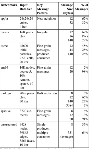
FIGURE 3. This figures compares the execution time of seven NIs on our seven macrobenchmarks. Both (a) and (b) are normalized to the AP3000-like NI with number of flow control buffers = 8. # buffers denotes the number of flow control buffers. (a) compares the performance of our three fifo-based NIs for different levels of flow control buffering. The black shade represents the execution time with infinite flow control buffering. Lighter shades represent the incremental execution time penalty for three flow control buffering levels (8, 2, and 1). (b) compares the performance of four coherent network interfaces with number of flow control buffers = 2. I However, because these NIs themselves provide plentiful buffering, their performance is largely insensitive to the number of flow control buffers. MC-like NI denotes the Memory Channel-like NI.
MC -like NI Start-JR-like NI CNI 512 Q CNI 32 Qm MC-like NI Start-JR-like NI CNI 512 Q CNI 32 Qm MC-like NI Start-JR-like NI CNI 512 Q CNI 32 Qm MC-like NI Start-JR-like NI CNI 512 Q CNI 32 Qm MC-like NI Start-JR-like NI CNI 512 Q CNI 32 Qm MC-like NI Start-JR-like NI CNI 512 Q CNI 32 Qm MC-like NI Start-JR-like NI CNI 512 Q CNI 32 Qm 0.0 0.2 0.4 0.6 0.8 1.0
Normalized Execution Time
CM-5-like NI Udma-based NI AP3000-like NI CM-5-like NI Udma-based NI AP3000-like NI CM-5-like NI Udma-based NI AP3000-like NI CM-5-like NI Udma-based NI AP3000-like NI CM-5-like NI Udma-based NI AP3000-like NI CM-5-like NI Udma-based NI AP3000-like NI CM-5-like NI Udma-based NI AP3000-like NI 0.0 1.0 2.0 3.0
Normalized Execution Time
# buffers = infinite # buffers = 8 # buffers = 2 # buffers = 1
tocols—that is, both message passing and shared memory—conse-quently have the same behavior.
We divide our discussion into two parts and examine the results in detail. First, we discuss the performance of the CM-5-like NI, the Udma-based NI, and the AP3000-like NI (Section 6.2.1). These NIs rely on NI memory to buffer network messages (via the flow control buffers). These three NIs are fifo-based NIs, but differ in the way they pop/push data to the fifos. For such push and pop the CM-5-like NI uses uncached loads/stores, the Udma-based NI uses User-Level DMA (or UDMA), and AP3000-like uses block loads/stores.
Second, we discuss the Memory Channel-like NI, the Start-JR-like NI, CNI512Q, and CNI32Qm, (Section 6.2.2). These NIs vide plentiful buffering in main memory without requiring a pro-cessor’s involvement. All these four NIs are either fully coherent or partially coherent. They differ primarily in the way the NI queues are allocated. The Memory Channel-like NI allocates receive queues in main memory. The Start-JR-like NI allocates both send and receive queues in main memory. CNI512Q allocates the queues in dedicated CNI memory. Finally, CNI32Qm allocates queues in main memory, but caches them in a CNI cache.
6.2.1 Comparison of Three Fifo-based NIs
Figure 3a compares the execution time for the three fifo-based NIs. The black bars, which show the execution time for the three NIs for infinite flow control buffering, allow us to isolate the impact of the data transfer parameters on the macrobenchmarks. With infi-nite flow control buffering, the Udma-based NI outperforms the CM-5-like NI by 0-15% and the AP3000-like NI outperforms the Udma-based NI by 11-44%. The Udma-based NI performs similar to or better than the CM-5-like NI because it uses the UDMA mechanism only for large payloads and falls back on uncached loads and stores, like the CM-5-like NI, for smaller messages. The AP3000-like NI’s lower latency and greater bandwidth (Section 6.1) clearly help improve the macrobenchmarks’ perfor-mance.
The lighter bars in Figure 3a show the increase in execution time as we reduce the number of flow control buffers. Clearly, the num-ber of flow control buffers have a significant impact on perfor-mance. Figure 3a shows two interesting results about flow control buffering. First, for all three NIs and all of our seven applications, increasing the number of flow control buffers from one to two sig-nificantly improves performance (between 6-40%). However, increasing the number of flow control buffers beyond two buys only modest performance gains (less than 19%) for most applications, except em3d and spsolve.
Second, the number of flow control buffers has significant impact on em3d and spsolve. This is because both em3d and spsolve generate bursts of small messages (less than 20 bytes) more rapidly than the receiving NI can consume. Consequently, the lack of flow control buffers has a dramatic impact on performance. For em3d and spsolve increasing the number of flow control buffers from two to infinity improves performance by 29-40% and 78-101% respectively for the three NIs. Actually, increasing the num-ber of flow control buffers to 128 for em3d and 33 for spsolve cap-tures most of the performance gains that can be achieved from an infinite number of flow control buffers.
6.2.2 Comparison of Four Coherent Network Interfaces
Figure 3b compares the execution time (normalized to the AP3000-like NI for flow control buffers = 8) of four NIs that are either partially or fully coherent. These NIs provide NI-managed, plentiful buffering in main memory on the receive side. Conse-quently, these NIs are largely insensitive to the number of flow con-trol buffers.Figure 3b shows three interesting results. First, the performance of the Memory Channel-like NI varies widely for the seven mac-robenchmarks. It performs significantly better than the AP3000-like NI, with the number of flow control buffers = 8, for em3d and spsolve because it provides plentiful buffering in main memory without direct processor involvement. It performs almost similar to the AP3000-like NI for appbt, barnes, dsmc, and moldyn because these macrobenchmarks do not gain significantly from plentiful buffering. It performs worse than the AP3000-like NI for unstruc-tured because unstrucunstruc-tured’s large messages effectively use the greater bandwidth provided by the AP3000-like NI (Table 5).
Second, among the four NIs shown in Figure 3b, the Memory Channel-like NI performs the worst and CNI32Qm performs the best. CNI32Qm—the CNI with a cache—outperforms the Memory Channel-like NI by 2-26% for the seven macrobenchmarks due to its lower latency and higher bandwidth (Table 5). CNI32Qm also outperforms The AP3000-like NI—the best fifo-based NI—and CNI512Q—the CNI with queues allocated in main memory—for all applications, except unstructured. It appears that the most important feature of unstructured’s communication is to stream data from the sender to the receiver. Both the AP3000-like NI and CNI512Q has less overhead for this data streaming compared to CNI32Qm, which incurs extra overhead due to its cache management (e.g. cache replacement). Consequently, CNI32Qm performs marginally worse than the AP3000-like NI and CNI512Q for unstructured. Like Mukherjee, et al. [29], we find that CNI32Qm is competitive with CNI512Q with much less memory.
Third, a comparison of the Start-JR-like NI and CNI32Qm shows that caching messages in a CNI cache, as in CNI32Qm, provides a performance boost of 2-13% for the seven macrobenchmarks. An examination of NI-related memory bus transactions reveals that CNI32Qm reduces the number of main memory to processor cache transactions by 54% (averaged across the seven macrobenchmarks). This is because CNI32Qm provides messages to the processor via direct CNI-cache-to-processor-cache transfers. Further, as the per-formance gap between microprocessors and main memory widens, we expect CNI32Qm to provide significantly better performance than the Start-JR-like NI because of two reasons. First, because CNI32Qm caches are small, they can be built with faster SRAMs, thereby providing lower latency to transfer messages. Second, CNI32Qm satisfies more than 50% of the processor’s accesses to the NI directly from its cache, which avoids message steering via main memory.
Overall, we find that CNI32Qm—the coherent interface with a cache—performs the best because it optimizes all of the five data transfer and buffering parameters. In summary, CNI32Qm:
•
effectively uses the block transfer mechanism of current memory buses by transferring messages in cache blocks;•
minimizes processor involvement for data transfer by initiating the transfer using a cachable store and decoupling the processor and NI via memory-mapped, cachable queues;•
directly transfers messages from the NI cache to the processor cache in the common case;•
provides plentiful buffering in main memory; and•
allows the NI to directly deposit messages into main memory, when the NI cache overflows.6.3 Single-Cycle NI
2wvs. CNI
32Q
mFigure 4 compares the performance of CNI32Qmwith an NI2w NI, whose memory can be accessed by the processor in a single cycle. Thus, our single-cycle NI2w approximates
processor-register-mapped NIs in research machines, such as the MIT M-machine [14].1
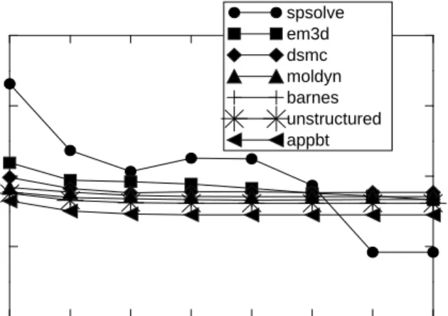
Figure 4 shows two interesting results. First, CNI32Qm—the CNI with a cache—outperforms our single-cycle NI2w for spsolve and em3d for small number of flow control buffers. Processor-regis-ter-mapped NIs are likely to have a small number of flow control buffers because of two reasons. First, a processor’s register memory is a precious resource and its size is severely constrained by its access time. Second, the demands of multiprogramming require that the NI2w buffers be either partitioned among multiple processes or saved and restored across context switches. The first solution limits the number of flow control buffers allocated per process and the second solution increases the context-switch time. Further, our single-cycle NI2w cannot also rely on commercial NIs for plentiful buffering (see Table 1). Consequently, CNI32Qm’s ability to buffer messages in NI caches and main memory without processor involvement makes its performance better or comparable to the sin-gle-cycle NI2w for spsolve and em3d. For example, for flow control buffers = 2, CNI32Qm’s performance is better than the single-cycle NI2w by 18% for spsolve and comparable for em3d. For spsolve and em3d, the breakeven point between CNI32Qm and the single-cycle NI2w occurs when the number flow control buffers equals 32 and 2 respectively.
Second, for the five macrobenchmarks other than spsolve and em3d, CNI32Qm is within 15% of the performance of the single-cycle NI2w (averaged across the five macrobenchmarks).
The above results suggest that in the absence of adequate buffer-ing, mapping an NI directly to the processor registers may not always be the optimal design point. Perhaps a two-level register memory hierarchy for NI registers can make such processor-regis-ter-mapped NIs competitive with a memory bus NI, such as CNI32Qm.
7 Related Work
To the best of our knowledge, this paper is the first to systemati-cally identify, examine, and explore the data transfer and buffering parameters that underlie the design of high-performance NIs for
1. Unlike our single-cycle NI2w, a processor in the MIT M-machine can compute directly from the NI registers, which allows zero-cycle access to the NI registers for some cases.
fine-grain communication. Mukherjee, et al. [29] examined NI2w and four Coherent Network Interfaces (including CNIiQm and CNIiQ) and found that transferring messages in cache block units and buffering messages in coherent memory space can improve per-formance. However, they neither examined alternative block trans-fer or buftrans-fering mechanisms nor evaluated the key parameters that affect the performance of such NIs.
Karamcheti and Chien [21] compared the messaging support in TMC CM-5 and Cray T3D and concluded that requiring processor involvement for message reception can significantly degrade per-formance. We improve upon their work by exposing and examining the design space of data transfer and buffering parameters. Blum-rich, et al. [3] compared the SHRIMP I and SHRIMP II NIs, but did not explore alternate data transfer and buffering mechanisms. Mackenzie, et al. [25] studied the effect of buffering using a syn-thetic workload and concluded that buffering messages in virtual memory can occur only rarely for realistic applications. However, in contrast we found that for two of our seven macrobenchmarks, buffering can play a significant role in improving performance. Henry and Joerg [18] compared the performance of three NIs mapped respectively to the processor registers, L1 cache bus, and an off-chip L2 cache bus. However, unlike our study, they did not examine the impact of buffering on the performance of these NIs.
8 Conclusions
In this paper we have systematically identified, examined, and explored the key parameters that affect the design of high-perfor-mance NIs targeted for fine-grain communication. We classified these parameters into two categories: data transfer and buffering parameters. The data transfer parameters capture how messages are transferred between internal memory structures (e.g. processor caches, main memory) of a computer and a memory bus NI. The buffering parameters capture where and how an NI buffers incom-ing network messages. We found that each of the three data transfer parameters—size of transfer, degree of processor involvement for transfer, and source/destination of transfer—and two buffering parameters—location of buffers and degree of processor involve-ment for buffering—can have a significant impact on performance.
Using two microbenchmarks and seven macrobenchmarks we evaluated seven memory bus NIs that we believe captured the essential components of the design space exposed by the five data transfer and buffering parameters. These seven NIs abstract the data transfer and buffering parameters of the NIs in TMC CM-5, Fujitsu AP3000, Princeton User-Level DMA, Digital Memory Channel, MIT StarT-JR, and two Coherent Network Interfaces—CNI512Q and CNI32Qm—proposed by Mukherjee, et al. [29].
Overall, we found that among these seven NIs, CNI32Qm—a coherent network interface that treats memory on the interface as a cache—performed the best because it optimizes all five data trans-fer and buftrans-fering parameters. It:
•
effectively uses the block transfer mechanism of current memory buses by transferring messages in cache blocks,•
minimizes processor involvement for data transfer by initiating the transfer using a cachable store and decoupling the processor and NI via memory-mapped, cachable queues,•
directly transfers messages from the NI cache to the processor cache in the common case,•
provides plentiful buffering in main memory, and•
allows the NI to directly deposit messages into main memory, when the NI cache overflows.As a corollary of this study, we found that, contrary to
conven-FIGURE 4. This figure compares the execution time of a single-cycle NI2w for different levels of flow control buffering. The vertical axis is normalized to the CNI32Qm on the memory bus. CNI32Qm is independent of flow control buffering because it provides plentiful buffering in main memory.
1 2 4 8 16 32 64 128
Number of Flow Control Buffers 0.0
0.5 1.0 1.5 2.0
Normalized Execution Time
spsolve em3d dsmc moldyn barnes unstructured appbt