© 2013-2020 SignalCore, Inc. support@signalcore.com
SC5502A
50 MHz to 10 GHz RF Signal Source
PXI Express
SC5502A Operating & Programming Manual i
C
O N T E N T S
Important Information
1
Warranty 1
Copyright & Trademarks 1
International Materials Declarations 2
CE European Union EMC & Safety Compliance Declaration 2
Recycling Information 3
Warnings Regarding Use of SignalCore Products 3
Getting Started
4
Unpacking 4
Verifying the Contents of your Shipment 4
Setting Up and Configuring the SC5502A 4
Signal Connections 6
Indicator LEDs 7
SC5502A Theory of Operation
8
Output Amplitude Control 8
Frequency Synthesizer 9
Frequency Tuning Modes 10
Reference Clock Control 10
Harmonics and Range Operation 11
Device Standby and RF Enable 11
Default Startup Mode 11
SC5502A Programming Interface
12
Device Drivers 12
Using the Application Programming Interface (API) 12
Setting the SC5502A - Writing to Configuration Registers
13
Configuration Registers 13
SC5502A Operating & Programming Manual ii
Setting the System Active LED 14
Setting the Device Standby Mode 14
Setting the RF Frequency 14
Setting the RF Power 14
Setting the Synth Mode 14
Setting the RF Automatic Level Control (ALC) Mode 14
Setting the RF ALC DAC Value 15
Setting the Reference Clock 15
Setting the Reference DAC Value 15
Writing to the User EEPROM 15
Setting RF Output Enable 15
Storing the Startup State 15
Disabling the Auto Power Feature 15
Querying the SC5502A - Writing to Request Registers
17
Reading the Device Status 17
Reading the Device Temperature 18
Reading the Calibration EEPROM 18
Reading the User EEPROM 19
Reading the RF ALC DAC Value 19
Calibration EEPROM Map
20
Software API Library Functions
21
Constants Definitions 22
Type Definitions 22
Function Definitions and Usage 23
Calibration & Maintenance
30
SC5502A Operating & Programming Manual Rev 2.0 1
I
M P O R T A N T
I
N F O R M A T I O N
Warranty
This product is warranted against defects in materials and workmanship for a period of three years from the date of shipment. SignalCore will, at its option, repair or replace equipment that proves to be defective during the warranty period. This warranty includes parts and labor.
Before any equipment will be accepted for warranty repair or replacement, a Return Material Authorization (RMA) number must be obtained from a SignalCore customer service representative and clearly marked on the outside of the return package. SignalCore will pay all shipping costs relating to warranty repair or replacement.
SignalCore strives to make the information in this document as accurate as possible. The document has been carefully reviewed for technical and typographic accuracy. In the event that technical or typographical errors exist, SignalCore reserves the right to make changes to subsequent editions of this document without prior notice to possessors of this edition. Please contact SignalCore if errors are suspected. In no event shall SignalCore be liable for any damages arising out of or related to this document or the information contained in it.
EXCEPT AS SPECIFIED HEREIN, SIGNALCORE, INCORPORATED MAKES NO WARRANTIES, EXPRESS OR IMPLIED, AND SPECIFICALLY DISCLAIMS ANY WARRANTY OF MERCHANTABILITY OR FITNESS FOR A PARTICULAR PURPOSE. CUSTOMER’S RIGHT TO RECOVER DAMAGES CAUSED BY FAULT OR NEGLIGENCE ON THE PART OF SIGNALCORE, INCORPORATED SHALL BE LIMITED TO THE AMOUNT THERETOFORE PAID BY THE CUSTOMER. SIGNALCORE, INCORPORATED WILL NOT BE LIABLE FOR DAMAGES RESULTING FROM LOSS OF DATA, PROFITS, USE OF PRODUCTS, OR INCIDENTAL OR CONSEQUENTIAL DAMAGES, EVEN IF ADVISED OF THE POSSIBILITY THEREOF. This limitation of the liability of SignalCore, Incorporated will apply regardless of the form of action, whether in contract or tort, including negligence. Any action against SignalCore, Incorporated must be brought within one year after the cause of action accrues. SignalCore, Incorporated shall not be liable for any delay in performance due to causes beyond its reasonable control. The warranty provided herein does not cover damages, defects, malfunctions, or service failures caused by owner’s failure to follow SignalCore, Incorporated’s installation, operation, or maintenance instructions; owner’s modification of the product;
owner’s abuse, misuse, or negligent acts; and power failure or surges, fire, flood, accident, actions of
third parties, or other events outside reasonable control.
Copyright & Trademarks
Under the copyright laws, this publication may not be reproduced or transmitted in any form, electronic or mechanical, including photocopying, recording, storing in an information retrieval system, or translating, in whole or in part, without the prior written consent of SignalCore, Incorporated.
SignalCore, Incorporated respects the intellectual property rights of others, and we ask those who use our products to do the same. Our products are protected by copyright and other intellectual property
SC5502A Operating & Programming Manual Rev 2.0 2 laws. Use of SignalCore products is restricted to applications that do not infringe on the intellectual property rights of others.
“SignalCore”, “signalcore.com”, and the phrase “preserving signal integrity” are registered trademarks of SignalCore, Incorporated. Other product and company names mentioned herein are trademarks or trade names of their respective companies.
International Materials Declarations
SignalCore, Incorporated uses a fully RoHS compliant manufacturing process for our products. Therefore, SignalCore hereby declares that its products do not contain restricted materials as defined by European Union Directive 2011/65/EU (EU RoHS) in any amounts higher than limits stated in the directive. This statement is based on the assumption of reliable information and data provided by our component suppliers and may not have been independently verified through other means. For products sold into China, we also comply with the “Administrative Measure on the Control of Pollution Caused by
Electronic Information Products” (China RoHS). In the current stage of this legislation, the content of six hazardous materials must be explicitly declared. Each of those materials, and the categorical amount present in our products, are shown below:
組成名稱 Model Name 鉛 Lead (Pb) 汞 Mercury (Hg) 镉 Cadmium (Cd) 六价铬 Hexavalent Chromium (Cr(VI)) 多溴联苯 Polybrominated biphenyls (PBB) 多溴二苯醚 Polybrominated diphenyl ethers (PBDE) SC5502A
✓
✓
✓
✓
✓
✓
A
✓
indicates that the hazardous substance contained in all of the homogeneous materials for this product is below the limit requirement in SJ/T11363-2006. AnX
indicates that the particular hazardous substance contained in at least one of the homogeneous materials used for this product is above the limit requirement in SJ/T11363-2006.CE European Union EMC & Safety Compliance Declaration
The European Conformity (CE) marking is affixed to products with input of 50 - 1,000 VAC or 75 - 1,500 VDC and/or for products which may cause or be affected by electromagnetic disturbance. The CE marking symbolizes conformity of the product with the applicable requirements. CE compliance is a
manufacturer’s self-declaration allowing products to circulate freely within the European Union (EU). SignalCore products meet the essential requirements of Directives 2014/30/EU (EMC) and 2014/35/EU (product safety), and comply with the relevant standards. Standards for Measurement, Control and Laboratory Equipment include EN 61326-1:2013 and EN 55011:2009 for EMC, and EN 61010-1 for product safety.
SC5502A Operating & Programming Manual Rev 2.0 3
Recycling Information
All products sold by SignalCore eventually reach the end of their useful life. SignalCore complies with EU Directive 2012/19/EU regarding Waste Electrical and Electronic Equipment (WEEE).
Warnings Regarding Use of SignalCore Products
(1)PRODUCTS FOR SALE BY SIGNALCORE, INCORPORATED ARE NOT DESIGNED WITH COMPONENTS NOR TESTED FOR A LEVEL OF RELIABILITY SUITABLE FOR USE IN OR IN CONNECTION WITH SURGICAL IMPLANTS OR AS CRITICAL COMPONENTS IN ANY LIFE SUPPORT SYSTEMS WHOSE FAILURE TO PERFORM CAN REASONABLY BE EXPECTED TO CAUSE SIGNIFICANT INJURY TO A HUMAN.
(2)
IN ANY APPLICATION, INCLUDING THE ABOVE, RELIABILITY OF OPERATION OF THE SOFTWARE PRODUCTS CAN BE IMPAIRED BY ADVERSE FACTORS, INCLUDING BUT NOT LIMITED TO FLUCTUATIONS IN ELECTRICAL POWER SUPPLY, COMPUTER HARDWARE MALFUNCTIONS, COMPUTER OPERATING SYSTEM SOFTWARE FITNESS, FITNESS OF COMPILERS AND DEVELOPMENT SOFTWARE USED TO DEVELOP AN APPLICATION, INSTALLATION ERRORS, SOFTWARE AND HARDWARE COMPATIBILITY PROBLEMS, MALFUNCTIONS OR FAILURES OF ELECTRONIC MONITORING OR CONTROL DEVICES, TRANSIENT FAILURES OF ELECTRONIC SYSTEMS (HARDWARE AND/OR SOFTWARE), UNANTICIPATED USES OR MISUSES, OR ERRORS ON THE PART OF THE USER OR APPLICATIONS DESIGNER (ADVERSE FACTORS SUCH AS THESE ARE HEREAFTER COLLECTIVELY TERMED “SYSTEM FAILURES”). ANY APPLICATION WHERE A SYSTEM FAILURE WOULD CREATE A RISK OF HARM TO PROPERTY OR PERSONS (INCLUDING THE RISK OF BODILY INJURY AND DEATH) SHOULD NOT BE SOLELY RELIANT UPON ANY ONE COMPONENT DUE TO THE RISK OF SYSTEM FAILURE. TO AVOID DAMAGE, INJURY, OR DEATH, THE USER OR APPLICATION DESIGNER MUST TAKE REASONABLY PRUDENT STEPS TO PROTECT AGAINST SYSTEM FAILURES, INCLUDING BUT NOT LIMITED TO BACK-UP OR SHUT DOWN MECHANISMS. BECAUSE EACH END-USER SYSTEM IS CUSTOMIZED AND DIFFERS FROM SIGNALCORE' TESTING PLATFORMS, AND BECAUSE A USER OR APPLICATION DESIGNER MAY USE SIGNALCORE PRODUCTS IN COMBINATION WITH OTHER PRODUCTS IN A MANNER NOT EVALUATED OR CONTEMPLATED BY SIGNALCORE, THE USER OR APPLICATION DESIGNER IS ULTIMATELY RESPONSIBLE FOR VERIFYING AND VALIDATING THE SUITABILITY OF SIGNALCORE PRODUCTS WHENEVER SIGNALCORE PRODUCTS ARE INCORPORATED IN A SYSTEM OR APPLICATION, INCLUDING, WITHOUT LIMITATION, THE APPROPRIATE DESIGN, PROCESS AND SAFETY LEVEL OF SUCH SYSTEM OR APPLICATION.
SC5502A Operating & Programming Manual Rev 2.0 4
G
E T T I N G
S
T A R T E D
Unpacking
All SignalCore products ship in antistatic packaging (bags) to prevent damage from electrostatic discharge (ESD). Under certain conditions, an ESD event can instantly and permanently damage several of the components found in SignalCore products. Therefore, to avoid damage when handling any SignalCore hardware, you must take the following precautions:
• Ground yourself using a grounding strap or by touching a grounded metal object. • Touch the antistatic bag to a grounded metal object before removing the hardware
from its packaging.
• Never touch exposed signal pins. Due to the inherent performance degradation caused by ESD protection circuits in the RF path, the device has minimal ESD protection against direct injection of ESD into the RF signal pins.
• When not in use, store all SignalCore products in their original antistatic bags.
Remove the product from its packaging and inspect it for loose components or any signs of damage. Notify SignalCore immediately if the product appears damaged in any way.
Verifying the Contents of your Shipment
Verify that your SC5502A kit contains the following items: Quantity Item
1 SC5502A RF Signal Source
1 Software Installation USB Flash Drive
Setting Up and Configuring the SC5502A
The SC5502A is a designed for use in a PXIe or PXIe hybrid chassis. Chassis manufacturers must provide at least the minimum required per-slot power dissipation cooling capability to be compliant with the PXIe specifications. The SC5502A is designed to be sufficiently cooled in either all-PXIe chassis or PXIe hybrid chassis (PXI Express chassis with traditional PXI slots). However, certain environmental factors may degrade performance. Inadequate cooling can cause the temperature inside the RF housing to rise above the maximum for this product, leading to improper performance and potentially reducing product lifespan or causing complete product failure. Maintain adequate air space around the chassis at all times and keep the chassis fan filters clean and unobstructed.
Refer to your chassis manufacturer’s user manual for proper setup and maintenance of your PXIe or PXIe hybrid chassis. The SC5502A on-board temperature sensor should indicate a rise of no more than 20 °C above ambient temperature under normal operating conditions.
!
SC5502A Operating & Programming Manual Rev 2.0 5 The SC5502A is a PXIe-based RF signal source with all user I/O located on the front face of the module as shown in Figure 1. Each I/O location is discussed in further detail below.
SC5502A Operating & Programming Manual Rev 2.0 6
Signal Connections
All signal connections (ports) on the SC5502A are SMA-type. Exercise caution when fastening cables to the signal connections. Over-tightening any connection can cause permanent damage to the device.
The condition of your system‘s signal connections can significantly affect measurement accuracy and repeatability. Improperly mated connections or dirty, damaged or worn connectors can degrade measurement performance. Clean out any loose, dry debris from connectors with clean, low-pressure air (available in spray cans from office supply stores). If deeper cleaning is necessary, use lint-free swabs and isopropyl alcohol to gently clean inside the connector barrel and the external threads. Do not mate connectors until the alcohol has completely evaporated. Excess liquid alcohol trapped inside the connector may degrade measurement performance until fully evaporated (this may take several days).
Tighten all SMA connections to 5 in-lb max (56 N-cm max)
RF OUT This port outputs the tunable RF signal from the source. The connector is SMA female. The
nominal output impedance is 50 Ω.
REF OUT This port outputs the internal 10 MHz or 100 MHz reference clock. The connector is SMA female. This port is AC-coupled with a nominal output impedance of 50 Ω.
REF IN This port accepts an external 10 MHz reference signal, allowing an external source to synchronize the internal reference clock. The connector is SMA female. This port is AC-coupled with a nominal input impedance of 50 Ω. Maximum input power is +13 dBm.
PXI CLK10 This port outputs the 10 MHz chassis reference signal from the chassis backplane, allowing it to synchronize the internal reference clock. An MCX male to SMA male cable is required (but not supplied) to connect this port to the “ref in” port in order to use this reference for synchronization. This port may be enabled or disabled through a software switch to minimize possible clock noise when not in use. This port has a nominal output impedance of
50 Ω and drives 0 dBm into a 50 Ω load.
!
SC5502A Operating & Programming Manual Rev 2.0 7
Indicator LEDs
The SC5502A provides visual indication of important modes. There are two LED indicators on the unit. Their behavior under different operating conditions is shown in Table 1.
Table 1. LED indicator states.
LED
Color
Definition
STATUS Green “Power good” and all oscillators phase-locked STATUS Red One or more oscillators off lock
STATUS Off Power fault
ACTIVE Green/Off Device is open (green) /closed (off) , this indicator is also user programmable (see register map)
SC5502A Operating & Programming Manual Rev 2.0 8
S C 5 5 0 2 A
T
H E O R Y O F
O
P E R A T I O N
Output Amplitude Control
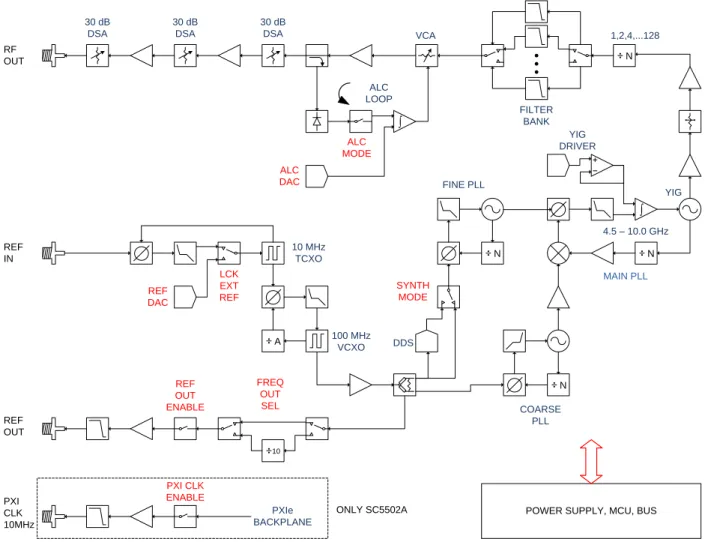
As shown in Figure 2, the SC5502A source architecture at a high level consists of an output amplitude control section and a frequency synthesis section. The amplitude of the signal is controlled through the use of digital step attenuators (DSAs) and a voltage controlled attenuator (VCA). The DSAs provide coarse-step tuning over a wide range while the VCA provides fine tune correction to the DSA. The VCA is part of the automatic level control loop (ALC), which additionally consists of an RF amplifier, a power detector, and an integrator. The ALC loop can be closed or open. In closed loop mode, the power detector outputs a voltage proportional to the power it detects. This voltage is compared to that of the reference ALC DAC voltage, which in turn is set for some calibrated power level. Voltage error between the detector voltage and the ALC DAC voltage drives the integrator output in the direction that will vary the VCA to achieve the desired output power level. When the ALC control loop is opened, the power detector output voltage is grounded, and the integrator is configured as a voltage buffer that drives the ALC DAC voltage to the VCA. In this mode, the ALC DAC voltage directly drives the VCA with voltage levels that correspond to calibrated output power levels.
There are advantages and disadvantages with either of these two amplitude control modes. On one hand, the open loop mode has an advantage over the closed loop mode when close-in carrier amplitude noise is a concern. ALC loops do introduce some level of amplitude modulated noise onto the carrier signal, and these levels may not be acceptable (although they are generally lower than the phase noise). SignalCore offers the option to open the ALC loop to remove any unwanted AM noise that results from closed loop control. Another side effect of the closed loop is that the frequency bandwidth of the ALC loop may slow down amplitude settling. Typically, in order to keep AM noise low and close (in offset frequency) to the signal, the loop bandwidth is also kept low. As a result, the settling time is increased. On the other hand, a closed loop ALC provides better amplitude control over the entire frequency range. With a temperature-stable ALC DAC, the closed loop will precisely maintain the power at the detector, mitigating errors in the components prior to it in the signal path. Temperature-induced errors in components and abrupt amplitude changes when switching filters in the filter banks contribute to errors in the amplitude of the signal. However, these errors occur before the power detector and are compensated by the feedback loop action. Errors in amplitude are thus confined to the output attenuators, amplifiers, and the loop components. When the loop is opened, amplitude errors resulting from all parts of the amplitude control section as well as the synthesizer section affect the overall output amplitude accuracy. In particular, when the filters within the filter bank are switched from one bank to another the signal experiences abrupt discontinuities in its amplitude which the open loop calibration cannot appropriately account for in its correction algorithm.
Setting of the amplitude control components is performed automatically by the system, although it is possible to override the ALC DAC value if needed. In Figure 2, the labels in red indicate parameters or devices which the user can directly control.
SC5502A Operating & Programming Manual Rev 2.0 9
Frequency Synthesizer
The synthesizer section of the SC5502A comprises a multiple phase-locked loop architecture whose base frequency reference is a 10 MHz TCXO. The user may choose to phase-lock this base reference to an external source if required. The 100 MHz VCXO is phase-locked to the TCXO for frequency stability. While the TCXO determines the very close-in phase noise, the VCXO phase noise determines the system phase noise in the frequency offset regions of approximately 1 kHz to 30 kHz. The 100 MHz VCXO provides the reference signal to the main RF signal synthesizer comprised of three phase-locked loops and a direct digital synthesis (DDS) oscillator. The “fine” PLL provides a tuning resolution of a few mHz over a narrow frequency range, while the “coarse” PLL tunes in steps of a few MHz over several GHz of
range. The “main” or summing PLL combines the signals of the “coarse”and “fine” loops into one broad
tuning signal with fine tuning.
Figure 2. Simplified block diagram of the SC5502A RF signal source.
Using this multiple loop approach produces signals with low phase noise and low phase spurs, high levels of which exist in single loop architectures such as single fractional-N PLLs. Although a single fractional-N type PLL may provide fine resolution, its large fractional spurs may make it unusable at certain parts of the band - especially at frequency regions close to the integer boundaries. A multiple
ALC DAC ALC MODE ALC LOOP FILTER BANK N N N N DDS FINE PLL MAIN PLL COARSE PLL 4.5 – 10.0 GHz YIG DRIVER A REF OUT REF IN REF DAC 10 MHz TCXO 100 MHz VCXO LCK EXT REF 10 1,2,4,...128 30 dB DSA 30 dB DSA 30 dB DSA FREQ OUT SEL REF OUT ENABLE SYNTH MODE PXI CLK 10MHz PXIe BACKPLANE PXI CLK ENABLE ONLY SC5502A VCA RF OUT YIG
SC5502A Operating & Programming Manual Rev 2.0 10 loop architecture allows for fine tuning with extremely low phase spurs. Furthermore, to improve the overall phase noise profile of the signal, a YIG-based oscillator anchors the main PLL instead of a diode-based VCO because of the YIG’s superior far-out phase noise performance in the frequency offset regions of 100 kHz to 10 MHz.
Frequency Tuning Modes
The synthesizer has two sets of control parameters that can be explored to optimize the device for a particular application. The first set of parameters, TUNE SPEED, sets the tuning and phase locking time as frequency is changed. TUNE SPEED comprises two modes - Fast Tune mode and Normal mode, both of which affect the YIG oscillator configuration. The Fast Tune mode deactivates a noise suppression capacitor across the tuning coil of the YIG oscillator. Doing so increases the rate of current flow through the coil and hence increases the available rate of frequency change. In Normal mode, the capacitor is activated, slowing down the available rate of frequency change. The advantage of activating the capacitor is that its presence in the circuit shunts the noise developed across the coil, decreasing close-in phase noise.
The other set of control parameters, FINE TUNE, sets the tuning resolution of the device. There are three modes to FINE TUNE: 1 MHz, 25 kHz, and 1 Hz steps. In the first two modes, the “fine” PLL uses the VCXO signal directly to synthesize its frequency and step size, while in the third mode it uses a DDS to provide 1 Hz resolution. The PLL-only modes provide the ability to realize exact frequencies with tuning as fine as 25 kHz. These modes offer several advantages including lower phase spurs and less computational demand required to set a new frequency. The 1 MHz mode has the lowest phase spurious signals, below the level of the product specifications. The DDS mode also tunes to exact frequencies. However, it requires many more computing cycles and several more internal device registers to write to in order to set a new frequency. Comparing setup times, the PLL-only modes require up to 175 microseconds to compute and setup the device for a new frequency, whereas the DDS mode can require up to 350 microseconds to perform the same action. At first glance it may seem that these differences could impact the frequency tuning times. However, the tuning times are predominantly set by the physical parameters of the YIG oscillator. Computation and register writes typically account for less than 25% of the total tune time of a 10 MHz step change in frequency.
Reference Clock Control
As mentioned above, the primary clock reference for the SC5502A is an onboard 10 MHz TCXO. Should the user require better frequency stability and/or accuracy, this TCXO can be programmed to phase-lock to an external source such as an OCXO or rubidium clock. The device can also be programmed to export either a 10 MHz or 100 MHz reference signal. To adjust the accuracy of the TCXO as needed, for example, to correct for long-term accuracy drift, the user may vary the reference DAC voltage by writing the REFERENCE_DAC_SETTING register.
The SC5502A can be programmed to lock to an external reference usually for better stability and accuracy, or for synchronizing the device to the reference. The reference source must be connected to the Ref In port. The device reference can be exported out the Ref Out port, and the user can choose to export a 10 MHz or 100 MHz signal.
SC5502A Operating & Programming Manual Rev 2.0 11 Additionally, the SC5502A routes the 10 MHz PXI chassis backplane clock to the front panel of the device. By cabling between the “PXI clk10” port and the “ref in” port, the user may enable the 10 MHz PXI chassis clock as a phase-locked reference for the SC5502A. A word of caution about the PXI chassis clock - the 10 MHz backplane clock is not considered to be a either a stable or accurate clock and could potentially have frequency errors in excess of +/- 40 ppm, significantly outside the locking range capability of the SC5502A.
Harmonics and Range Operation
The SC5502A’s guaranteed operating frequency range is 50 MHz to 10 GHz. At low frequencies of operation (200 MHz and lower), the harmonics of the signal can potentially be observed as high as -10 dBc at 0 dBm output. This is due to the limited space available for additional filtering in these ranges. At lower frequencies, the large physical size of appropriate filters makes it impossible to accommodate them within the compact form of this device. Furthermore, as the low frequencies are synthesized through frequency dividers, their output waveforms become more “square” than sinusoidal, giving rise to higher odd-order harmonics.
The device is specified to a maximum calibrated level of +10 dBm for frequencies up to 9 GHz, and to a maximum of +7 dBm for frequencies greater than 9 GHz, although the maximum calibrated output is greater than that in most regions of the spectrum. The accuracy degrades as the amplitude approaches the compression point due to the linear approximation in the correction algorithm. As a general rule, however, the lower the tuned frequency, the higher the achievable output power.
Device Standby and RF Enable
The SC5502A has both standby and RF output enable features. The user may wish to put the device into standby mode to reduce power consumption and thus lower the operating temperature of the device under the same environmental conditions. Taking the device out of standby requires the device to wait for the power rails to settle and all internal components to be reprogrammed, usually about one second. Disabling the RF output moves the frequency to some very low value so that the step attenuators (DSA) and voltage controlled attenuators (VCA) have the most effective attenuation. This will push the signal level below -100 dBm. Enabling the RF output is nearly instantaneous as all components remain active even when the output is disabled.
Default Startup Mode
The factory power-up state for the device is detailed in Table 2. The default state can be changed to the current state programmatically, allowing the user to power up the device in the last saved state without having to reprogram.
Table 2. Factory default power-up state.
Frequency 5.0 GHz Standby Disabled
Power 0.00 dBm Auto Level Enabled
RF Output Enabled Ref Out Disabled
SC5502A Operating & Programming Manual Rev 2.0 12
S C 5 5 0 2 A
P
R O G R A M M I N G
I
N T E R F A C E
Device Drivers
The SC5502A is programmed by writing to its set of configuration registers, and its status is read back through its set of query registers. The user may choose to program directly at register level or through the API library functions provided. These API library functions are wrapper functions of the registers that simplify the task of configuring of the register bytes. The register specifics are covered in the next section. Writing to and reading from the device at the register level through the API involves calls to the
sc5502a_RegWrite and sc5502a_RegRead functions respectively.
For Microsoft WindowsTM operating systems, The SC5502A API is provided as a dynamic linked library, sc5502a.dll. This API uses NI-VISATM to communicate with the device. Inclusion of the NI-VISA driver is required for code development in programming languages such C, C++, or LabVIEWTM. For LabVIEWTM support, an additional LabVIEW API, sc5502a.llb, is also provided. The functions in the LabVIEW API are primarily LabVIEW VI wrappers to the standard API functions. NI-VISATM is available from National Instruments Corporation (www.ni.com).
For other operating systems or VISA implementations such as Agilent VISA, users will need to access the device through their own proprietary PXIe driver. The VISA-based driver code is available to our customers by request. This code can be compiled with Agilent VISA with minimal or no code change. Should the user require assistance in writing an appropriate API other than that provided, please contact SignalCore for additional example code and hardware details.
Using the Application Programming Interface (API)
The SC5502A API library functions make it easy for the user to communicate with the device. Using the API removes the need to understand register-level details - their configuration, address, data format, etc., and the additional layer between the PXIe bridge and the onboard microcontroller that must be configured prior to writing the device registers. Using the API, commands to control the device are greatly simplified. For example, to obtain the device temperature, the user simply calls the function
sc5502A_GetDeviceTemperature or sc5502A_SetFrequency to tune the frequency. The software API is covered in detail in the “Software API Library Functions” section.
SC5502A Operating & Programming Manual Rev 2.0 13
S
E T T I N G T H E
S C 5 5 0 2 A
-
W
R I T I N G T O
C
O N F I G U R A T I O N
R
E G I S T E R S
Configuration Registers
Users may write the configuration registers (write only) directly by calling the sc5502a_RegWrite
function. The syntax for this function is sc5502a_RegWrite(deviceHandle, registerCommand, instructWord). The instructWord takes a 64 bit-word. However, it will only send the required number of bytes to the device. Table 3 summarizes the register addresses (commands) and the effective bytes of command data.
Table 3: Configuration registers.
Register Name Regist er Addre ss Serial
Range Bit 7 Bit 6 Bit 5 Bit 4 Bit 3 Bit 2 Bit 1 Bit 0
INITIALIZE 0x01 [7:0] Open Open Open Open Open Open Open Mode SET_SYSTEM_ACTIVE 0x02 [7:0] Open Open Open Open Open Open Open
Enable “active” LED DEVICE_STANDBY 0x05 [7:0] Open Open Open Open Open Open Open Mode
RF_FREQUENCY 0x10
[7:0] Fine Frequency Adjust Word [7:0] [15:8] Fine Frequency Adjust Word [15:8] [23:16] Fine Frequency Adjust Word [23:16] [31:24] Fine Frequency Adjust Word [31:24] [39:32] Fine Frequency Adjust Word [39:32] RF_POWER 0x11 [7:0] RF Power Word [7:0]
[15:8] Sign Bit RF Power Word [14:8]
SYNTH_MODE 0x12 [7:0] Fast
Tune Fine Tune Modes RF_ALC_MODE 0x13 [7:0] Open Open Open Open Open Open Open Mode SET_ALC DAC_VALUE 0x14 [7:0] ALC DAC Word [7:0]
[15:8] ALC DAC Word [13:8]
REFERENCE_MODE 0x15 [7:0] Open Open Open Open
PXI Clk 10 Enable 100 MHz Out Enable Ref Out Enable Lock Enable REFERENCE_DAC_SET TING 0x16
[7:0] REFERENCE DAC Word [7:0]
[15:8] Open Open REFERENCE DAC Word [13:8] USER_EEPROM_WRIT
E 0x23
[7:0] DATA [7:0]
[15:8] EEPROM Address [15:8] [23:16] EEPROM Address [23:16]
RF_OUT_ENABLE 0x26 [7:0] Open Open Open Open Open Open Open Mode STORE_STARTUP_STA
TE 0x28 [7:0] Open Open Open Open Open Open Open Open AUTO_POWER_DISAB
SC5502A Operating & Programming Manual Rev 2.0 14
Initializing the Device
INITIALIZE (0x01) - Writing 0x00 to this register will reset the device to the default power-on state. Writing 0x01 will reset the device but leave it in the current state. The user has the ability to define the default startup state by writing to the START UP STATE (0x28) register, described later in this section.
Setting the System Active LED
SET_SYSTEM_ACTIVE (0x02) - This register turns on the front panel “active” LED with a write of 0x01 or turns off the LED with a write of 0x00. This register is generally written when the device driver opens or closes the device.
Setting the Device Standby Mode
DEVICE_STANDBY (0x05) - Writing 0x01 to this register will power down the analog/RF circuitry. Writing 0x00 to this register will enable the analog/RF circuitry and the device will return to its last programmed state.
Setting the RF Frequency
RF_FREQUENCY (0x10) - This register sets the RF frequency. Data is sent as a 40 bit word with the LSB in Hz.
Setting the RF Power
RF_POWER (0x11) - This register sets the RF power level. The LSB is 1/100th of a dB and absolute magnitude is carried in the first 15 bits, starting with bit 0. The sign bit is indicated on bit 15. Setting bit 15 high implies a negative magnitude. For example, to write 10.05 dBm to the register, the data is 1005 (0x03ED). For -10.05 dBm, the data is 33773 (0x83ED).
Setting the Synthesizer Mode
SYNTH_MODE (0x12) - This register has one data byte and provides two tuning modes for the device - Fast Tune and Fine Tune. By default the Fast Tune is disabled (normal mode). Asserting high bit 2 of the data byte will enable Fast Tune. Fast Tune enables the device for faster lock and settling times between frequency changes. The Fine Tune mode has 3 options - 1 MHz (PLL), 25 kHz (PLL), and 1 Hz (DDS). Selection of these options requires setting the first 2 bits of the data byte to 0, 1, and 2, respectively. See the “Frequency Tuning Modes” section for more information. As an example, to set the device for Fast Tune and step at 1 Hz resolution, write 0x06.
Setting the RF Automatic Level Control (ALC) Mode
RF_ALC_MODE (0x13) - Writing 0x00 to this register puts the ALC in a closed loop operation. Writing 0x01 will run the ALC in an open loop. See the “Output Amplitude Control” section to understand the differences between the modes.
SC5502A Operating & Programming Manual Rev 2.0 15
Setting the RF ALC DAC Value
RF_ALC_DAC_SETTING (0x14) - Writing a 14 bit control word to the ALC DAC register adjusts output amplitude. This is useful when the user wants to make small adjustments to the power level.
Setting the Reference Clock
REFERENCE_MODE (0x15) - This register sets the behavior of the reference clock section. Bit 3 enables (1) or disables (0) the PXI 10 MHz clock, Bit 2 selects whether the output reference signal is 10 MHz (0) or 100 MHz (1), Bit 1 enables (1) or disables (0) the output reference signal, and Bit 0 enables (1) or disables (0) the device to phase-lock to an external source. It is important that if the device is not intended to lock externally, the external source connection should be removed from the “ref in”
connector. Even with external locking disabled, the presence of a large signal from the external source on the reference input terminal could potentially modulate the internal references, causing a spur offset in the RF signal.
Setting the Reference DAC Value
REFERENCE_DAC_SETTING (0x16) - The frequency precision of the device’s 10 MHz TCXO is set by the device internally and the factory calibrated unsigned 14 bit value is written to the reference DAC on power-up from the EEPROM. The user may choose to write a different value to the reference DAC by accessing this register, for example, to correct for long-term accuracy drift.
Writing to the User EEPROM
WRITE_USER_EEPROM (0x23) - There is an onboard 32 kilobyte EEPROM for the user to store data. User data is sent one byte at a time and is contained in the last (least significant) of the three bytes of data written to the register. The other two bytes contain the write address in the EEPROM. For example, to write user data 0x22 into address 0x1F00 requires writing 0x1F0022 to this register.
Setting RF Output Enable
RF_OUT_ENABLE (0x26) - This register enables or disables the RF signal output. Setting bit 0 low (0) disables RF output. Setting bit 0 high (1) enables RF output.
Storing the Startup State
STORE_STARTUP_STATE (0x28)– Writing to this register will save the current device state as the new default power on (startup) state. All data written to this register will be ignored as only the write command is needed to initiate the save.
Disabling the Auto Power Feature
AUTO_POWER_DISABLE (0x29) - When changing frequency, the device will calculate new settings for the amplitude control components such that the amplitude remains the same as the last setting. If the
SC5502A Operating & Programming Manual Rev 2.0 16 amplitude is also changed at the new frequency setting, the user has the option to turn off this auto power adjustment. By default, auto power adjust is enabled. To disable this feature, set bit 0 high (1).
SC5502A Operating & Programming Manual Rev 2.0 17
Q
U E R Y I N G T H E
S C 5 5 0 2 A
-
W
R I T I N G T O
R
E Q U E S T
R
E G I S T E R S
The registers to read data back from the device (such as device status) are accessed through the
sc5502a_RegRead function. The function and parameter format for this command is
sc5502a_RegRead(deviceHandle, registerCommand, instructWord,*dataOut). Any instructions in
addition to the register call are placed into “instructWord”, and data obtained from the device is
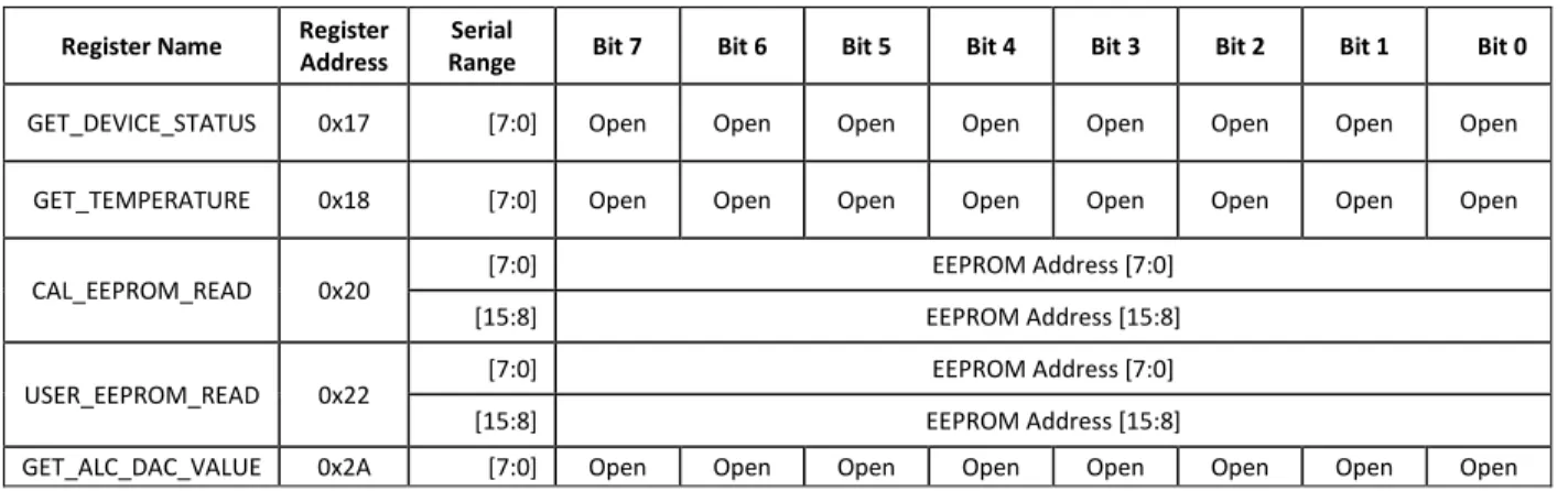
returned via the pointer value dataOut. The set of request registers are shown in Table 4.
Table 4: Query registers.
Register Name Register Address
Serial
Range Bit 7 Bit 6 Bit 5 Bit 4 Bit 3 Bit 2 Bit 1 Bit 0
GET_DEVICE_STATUS 0x17 [7:0] Open Open Open Open Open Open Open Open GET_TEMPERATURE 0x18 [7:0] Open Open Open Open Open Open Open Open
CAL_EEPROM_READ 0x20 [7:0] EEPROM Address [7:0] [15:8] EEPROM Address [15:8] USER_EEPROM_READ 0x22 [7:0] EEPROM Address [7:0]
[15:8] EEPROM Address [15:8]
GET_ALC_DAC_VALUE 0x2A [7:0] Open Open Open Open Open Open Open Open
Reading the Device Status
GET_DEVICE_STATUS (0x17) - This register, summarized in Table 5, returns the device status information such as phase lock status of the PLL, current reference settings, etc. Data is contained in the first three bytes.
Table 5. Description of the status data bits.
Bit Description
[15] 10 MHz TCXO PLL lock status [14] 100 MHz VCXO PLL lock status [13] Main PLL lock status
[12] Reserved [11] Reserved
[10] Fine PLL lock status [9] Coarse PLL lock status [8] Reserved
[7] External reference detected [6] Reference output enabled [5] Reference lock enabled
SC5502A Operating & Programming Manual Rev 2.0 18
Bit Description
[4] ALC mode [3] Fast tune state [2] Device standby state [1] RF out state
[0] PXI clock state
Reading the Device Temperature
GET_TEMPERATURE (0x18) - Data returned by this register needs to be processed to correctly represent data in temperature units of degrees Celsius. Data is returned in the first 14 bits [13:0]. Bit [13] is the polarity bit indicating whether it is positive (0x0) or negative (0x1). The temperature value represented in the raw data is contained in the next 13 bits [12:0]. To obtain the temperature ADC code, the raw
data should be masked (bitwise AND’ed) with 0x1FFF, and the polarity should be masked with 0x2000.
The conversion from 12 bit ADC code to an actual temperature reading in degrees Celsius is shown below:
Positive Temperature (bit 13 is 0) = ADC code / 32
Negative Temperature (bit 13 is 1) = (ADC code – 8192) / 32
It is not recommended to read the temperature too frequently, especially once the SC5502A has stabilized in temperature. The temperature sensor is a serial device located inside the RF module. Therefore, like any other serial device, reading the temperature sensor requires sending serial clock and data commands from the processor. The process of sending clock pulses on the serial transfer line may cause unwanted spurs on the RF signal as the serial clock could potentially modulate the internal oscillators. Furthermore, once the SC5502A stabilizes in temperature, repeated readings will likely differ by as little as 0.25 °C over extended periods of time. Given that the gain-to-temperature coefficient is on the order of less than -0.01 dB/°C, gain changes between readings will be negligible.
Reading the Calibration EEPROM
CAL_EEPROM_READ (0x20) - Reading a single byte from an address in the device EEPROM is performed
by writing this register with the address for the instructWord. The data is returned as a byte. The CAL EEPROM maximum address is 0x7FFF. Reading above this address will cause the device to retrieve data from the lower addresses. For example, addressing 0x8000 will return data stored in address location 0x0000. The calibration EEPROM map is shown in Table 6. Calibration EEPROM map.
All calibration data, whether floats, unsigned 8-bit, unsigned 16-bit or unsigned 32-bit integers, are stored as flattened unsigned byte representation. A float is flattened to 4 unsigned bytes, so once it is read back it needs to be un-flattened back to its original type. Unsigned values containing more than a single byte are converted (un-flattened) simply by concatenation of the bytes through bit-shifting. Converting to floating point representation is slightly more involved. First, convert the 4 bytes into an
SC5502A Operating & Programming Manual Rev 2.0 19 unsigned 32-bit integer value, and then (in C/C++) type-cast a float pointer to the address of the value. In C/C++, the code would be float Y = *(float *)&X, where X has been converted earlier to an unsigned integer.
An example written in C code would look something like the following:
Reading the User EEPROM
USER_EEPROM_READ (0x22) - Once data has been written to the user EEPROM, it can be retrieved by
calling this register and using the process outlined above for reading calibration data. The maximum address for this EEPROM is also 0x7FFF.
Reading the RF ALC DAC Value
GET_ALC_DAC_VALUE (0x2A) - The user may be interested to obtain the current value of the ALC DAC
for the purpose of making minor adjustments to the RF output power level. Data is returned in the first 14 bits.
byte_value[4]; // read in earlier
unsigned int uint32_value; float float32_value; int count = 0; while (count < 4) {
uint32_value = unit32_value | (byte_value[count] << (count*8));
count++; }
SC5502A Operating & Programming Manual Rev 2.0 20
C
A L I B R A T I O N
E E P R O M
M
A P
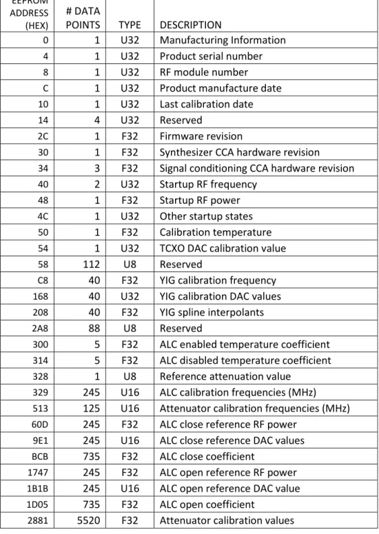
Table 6. Calibration EEPROM map.
EEPROM ADDRESS (HEX)
# DATA
POINTS TYPE DESCRIPTION
0 1 U32 Manufacturing Information 4 1 U32 Product serial number
8 1 U32 RF module number
C 1 U32 Product manufacture date 10 1 U32 Last calibration date
14 4 U32 Reserved
2C 1 F32 Firmware revision
30 1 F32 Synthesizer CCA hardware revision
34 3 F32 Signal conditioning CCA hardware revision 40 2 U32 Startup RF frequency
48 1 F32 Startup RF power
4C 1 U32 Other startup states 50 1 F32 Calibration temperature 54 1 U32 TCXO DAC calibration value
58 112 U8 Reserved
C8 40 F32 YIG calibration frequency 168 40 U32 YIG calibration DAC values 208 40 F32 YIG spline interpolants
2A8 88 U8 Reserved
300 5 F32 ALC enabled temperature coefficient 314 5 F32 ALC disabled temperature coefficient 328 1 U8 Reference attenuation value
329 245 U16 ALC calibration frequencies (MHz) 513 125 U16 Attenuator calibration frequencies (MHz) 60D 245 F32 ALC close reference RF power
9E1 245 U16 ALC close reference DAC values BCB 735 F32 ALC close coefficient
1747 245 F32 ALC open reference RF power 1B1B 245 U16 ALC open reference DAC value 1D05 735 F32 ALC open coefficient
SC5502A Operating & Programming Manual Rev 2.0 21
S
O F T W A R E
A P I
L
I B R A R Y
F
U N C T I O N S
SignalCore’s philosophy is to provide products to our customers whose lower hardware functions are
easily accessible. Having the ability to access the registers directly is a necessity for those who wish to use direct low-level control of frequency and gain settings. However, others may wish for simpler product integration by using higher level function libraries and by not programming registers directly. The functions provided in the SC5502A API dynamic-linked (Windows operating systems), shared (Linux operating system), or LabVIEW library are:
• sc5502a_SearchDevices • sc5502a_OpenDevice • sc5502a_CloseDevice • sc5502a_RegWrite • sc5502a_RegRead • sc5502a_InitDevice • sc5502a_SetStandby • sc5502a_SetFrequency • sc5502a_SetPowerLevel • sc5502a_SetReferenceClock • sc5502a_SetReferenceDac • sc5502a_SetSynthesizerMode • sc5502a_SetAlcDac • sc5502a_SetCurrentUpState • sc5502a_WriteUserEeprom • sc5502a_GetDeviceStatus • sc5502a_GetDeviceAttributes • sc5502a_GetTemperature • sc5502a_ReadCalEeprom • sc5502a_ReadUserEeprom • sc5502a_GetAlcDac
Each of these functions is described in more detail on the following pages. First, for C/C++ we define the constants and types which are contained in the C header file, sc5502a.h. These constants and types are useful not only as an include for developing user applications using the SC5502a API, but also for writing device drivers independent of those provided by SignalCore.
SC5502A Operating & Programming Manual Rev 2.0 22
Constants Definitions
// Parameters for storing data in the onboard EEPROMs
#define CALEEPROMSIZE 32768 // size in bytes
#define USEREEPROMSIZE 32768 // size in bytes // Synthesizer fine tune modes
#define DISABLEDFINEMODE 0 // 1 MHz tuning steps, PLL implementation
#define PLLFINEMONDE 1 // 25 kHz tuning steps, PLL implementation
#define DDSFINEMODE 2 // 1 Hz tuning steps, DDS implementation // Error set #define RESERVEDERROR -1 #define NOTCORRECTDEVICE -2 #define INPUTNULL -3 #define COMMERROR -4 #define INPUTNOTALLOC -5 #define EEPROMOUTBOUNDS -6 #define INVALIDARGUMENT -7 #define INPUTOUTRANGE -8 #define NOREFWHENLOCK -9 #define NORESOURCEFOUND -10 #define INVALIDCOMMAND -11
// Define device registers
#define INITIALIZE 0x01 // initialize the device
#define SET_SYSTEM_ACTIVE 0x02 // set the device “active” LED
#define POWER_STANDBY 0x05 // place the device into standby mode
#define RF_FREQUENCY 0x10 // set the frequency
#define RF_POWER 0x11 // set the power level of the RF output
#define SYNTH_MODE 0x12 // synth mode control
#define RF_ALC_MODE 0x13 // closed or open loop ALC mode
#define RF_ALC_DAC 0x14 // set the RF ALC DAC value
#define REFERENCE_SETTING 0x15 // reference clock settings
#define REFERENCE_DAC_WORD 0x16 // set reference clock DAC
#define GET_DEVICE_STATUS 0x17 // read the device status
#define GET_TEMPERATURE 0x18 // get the internal temperature of he device
#define CAL_EEPROM_READ 0x20 // read a byte from the calibration EEPROM
#define CAL_EEPROM_WRITE 0x21 // cal EEPROM write (not accessible)
#define USER_EEPROM_READ 0x22 // read a byte from the user EEPROM
#define USER_EEPROM_WRITE 0x23 // write a byte to the user EEPROM
#define RF_POWER_MODE 0x26 // enable RF output
#define START_UP_STATE 0x28 // store new default state
#define AUTO_PWR_MODE 0x29 // disable auto power leveling
Type Definitions
typedef struct deviceInfo_t {
unsigned int productSerialNumber;
unsigned int rfModuleSerialNumber;
float firmwareRevision;
float synthHardwareRevision;
float signalHardwareRevision;
unsigned int calDate; // year, month, day, hour:&(0xFF000000,0x00FF0000, 0x0000FF00,0x000000FF)
SC5502A Operating & Programming Manual Rev 2.0 23
unsigned int manDate; // year, month, day, hour:&(0xFF000000,0x00FF0000, 0x0000FF00,0x000000FF)
} deviceInfo_t;
typedef struct deviceStatus_t {
bool tcxoPllLock; // Master 10 MHz TCXO
bool vcxoPllLock; // 100 MHz VCXO
bool finePllLock; // Fine Tuning PLL
bool coarsePllLock; // Coarse tuning PLL
bool sumPllLock; // Main tuning PLL
bool extRefDetected; // Indicates whether an external source is detected
bool refClkOutEnable; // Indicates if the reference output port is enabled
bool extRefLockEnable; // Indicates if the TCXO lock is enabled
bool alcOpen; // Indicates that the ALC is in open loop
bool fastTuneEnable; // Indicates if tuning mode is enabled
bool standbyEnable; // Power down of analog circuit
bool rfEnable; // RF port is enabled
bool pxiClkEnable; // PXI 10 MHz port is enabled
} deviceStatus_t;
Function Definitions and Usage
The functions listed below are found in the sc5502a.dll dynamic linked library for the WindowsTM operating system. These functions are also provided in the LabVIEW library, sc5502a.llb. The LabVIEW functions contain context help (Ctrl+H) to assist with connecting the input and output parameters.
Function: sc5502a_ListResources
Definition: int sc5502a_ListResources (char **visaResource, unsignedint *size)
Output: char **visaResource (pointer list to visaResource)
unsignedint *size (the numbers of devices found) Description: sc5502a_ListResources searches for SignalCore SC5502A devices connected to the host computer and returns an array containing their VISA resource names. The user can use this information to open the device(s) with the resource name of choice. See
sc5502a_OpenDevice function on how to open a device.
Function: sc5502a_OpenDevice
Definition: int sc5502a_OpenDevice (char *visaResource, unsignedint *deviceHandle)
Input: char*visaResource (pointer list to visaResource)
Output: unsignedint *deviceHandle (unsigned int number for the deviceHandle) Description: sc5502a_OpenDevice opens the device and turns the front panel “active” LED on if
successful. It returns a handle to the device for other function calls.
Function: sc5502a_CloseDevice
SC5502A Operating & Programming Manual Rev 2.0 24 Input: unsignedint deviceHandle (handle to the device to be closed) Description: sc5502a_CloseDevice closes the device associated with the device handle and turns off
the “active” LED on the front panel if it is successful.
Example: Code to exercise the functions that open and and close the PXIe device:
Function: sc5502a_RegWrite
Definition: int sc5502a_RegWrite (unsignedint deviceHandle, unsignedchar commandByte, unsignedlonglongint instructWord)
Input: unsignedint deviceHandle (handle to the opened device)
unsignedchar commandByte (register address)
unsignedlonglongint instructWord (the data for the register) Description: sc5502a_RegWrite writes the instructWord data to the register specified by the
commandByte. See the register map on Table 3 for more information. Example: To set the power level to 2.00 dBm:
int status = sc5502a_RegWrite(devHandle, RF_POWER, 200);
// Declaring
char **visaResource = (char**)malloc(sizeof(char*)*100);
unsigned int deviceHandle;
int devicesFound;
int i,status;
// Allocate memory
for(i = 0; i< 100; i++)
visaResource[i] = (char*)malloc(sizeof(char)*1000); status = sc5502a_ListResources(visaResource, &devicesFound);
printf("There are %d SignalCore USB devices found. \n", devicesFound);
if(devicesFound == 0)
//If no device are found deallocate memory and end the program
{
for(i = 0; i<100;i++)
free(visaResource[i]); free(visaResource);
printf("No sc5502a devices detected. Press enter to continue.\n");
return 1; }
//** sc5502a_OpenDevice, open device 0
status = sc5502a_OpenDevice(visaResource[0], &deviceHandle); // Free memory
for(i = 0; i<100;i++)
free(visaResource[i]); free(visaResource);
//
// Do something with the device //
//Close the device
SC5502A Operating & Programming Manual Rev 2.0 25 Function: sc5502a_RegRead
Definition: int sc5502a_RegRead (unsignedint deviceHandle, unsignedchar commandByte, unsignedlonglongint instructWord, unsignedint *receivedWord)
Input: unsignedint deviceHandle (handle to the opened device)
unsignedchar commandByte (the address byte of the register to write to)
unsignedlonglongint instructWord (the data for the register)
unsignedint *receivedWord (data to be received) Description: sc5502a_RegRead reads the data requested by the instructWord data to the register
specified by the commandByte. See the register map on Table 4 for more information.
Example: To read the status of the device:
Function: sc5502a_InitDevice
Definition: int sc5502a_InitDevice (unsignedint deviceHandle, bool mode)
Input: unsignedintdeviceHandle (handle to the opened device)
boolmode (set the mode of initialization)
Description: sc5502A_InitDevice initializes (resets) the device. Mode = 0 resets the device to the default power up state. Mode = 1 resets the device but leaves it in its current state.
Function: sc5502a_SetStandby
Definition: int sc5502a_SetDeviceStandby(unsignedint deviceHandle, bool standbyStatus)
Input: unsignedintdeviceHandle (handle to the opened device)
boolstandbyStatus (set to true (1) to set device in standby mode) Description: sc5502a_SetStandby puts the device in standby mode where the power to the analog
circuits are disabled, conserving power.
Function: sc5502a_SetFrequency
Definition: int sc5502a_SetFrequency (unsignedint deviceHandle,
unsignedlonglongint frequency)
Input: unsignedintdeviceHandle (handle to the opened device)
unsignedlonglongintfrequency (frequency in Hz) Description: sc5502a_SetFrequency sets the RF frequency.
unsigned int deviceStatus;
int status = sc5502a_RegRead(devHandle,
SC5502A Operating & Programming Manual Rev 2.0 26 Function: sc5502a_SetPowerLevel
Definition: int sc5502a_SetPowerLevel(unsignedint deviceHandle, float power)
Input: unsignedint deviceHandle (handle to the opened device)
float power (set power in dBm) Description: sc5502a_SetPowerLevel sets the value of the desired output power level.
Function: sc5502a_SetRfOut
Definition: int sc5502a_SetRfOut(unsignedint deviceHandle, bool mode)
Input: unsignedint deviceHandle (handle to the opened device)
bool mode (disable/enable RF output)
Description: sc5502a_SetRfOutenables or disables the RF output.
Function: sc5502a_SetAlcMode
Definition: int sc5502a_SetAlcMode(unsignedint deviceHandle, bool mode)
Input: unsignedint deviceHandle (handle to the opened device)
bool mode (closed or open loop operation of the ALC circuit) Description: sc5502a_SetAlcMode sets the ALC loop to closed or open loop operation.
Function: sc5502a_SetAlcDac
Definition: int sc5502a_SetAlcDac(unsignedint deviceHandle, unsigned int dacValue)
Input: unsignedint deviceHandle (handle to the opened device)
unsigned intdacValue (14 bit value for adjusting the ALC DAC) Description: sc5502a_SetAlcDac writes a value to the ALC DAC to control the RF output level.
Function: sc5502a_SetSynthesizerMode
Definition: int sc5502a_SetSynthesizerMode(unsignedint deviceHandle,
bool fastTuneEnable, unsignedint fineTuneMode)
Input: unsignedint deviceHandle (handle to the opened device)
boolfastTuneEnable (enable/disable faster frequency stepping)
unsignedintfineTuneMode (selects 1 MHz, 25 kHz, or 1 Hz tuning step resolution) Description: sc5502a_SetSynthesizerMode enables/disables fast tuning and sets the step resolution
SC5502A Operating & Programming Manual Rev 2.0 27 Function: sc5502a_DisableAutoLevel
Definition: int sc5502a_DisableAutoLevel(unsignedint deviceHandle, bool mode)
Input: unsignedint deviceHandle (handle to the opened device)
boolmode (defines when to disable auto-level)
Description: sc5502a_DisableAutoLevel disables the device from auto adjusting the power level to the current state when frequency is changed. Disabling the auto adjust feature allows the device to return faster after calling sc5502a_SetPowerLevel. If the power remains the same for the next tuned frequency, this should not be disabled.
Function: sc5502a_SetReferenceClock
Definition: int sc5502a_SetClockReference(unsignedint deviceHandle, bool lockExtEnable,
bool refOutEnable, bool clk100Enable, bool pxiClk)
Input: unsignedint deviceHandle (handle to the opened device)
bool lockExtEnable (enables phase locking to an external source)
bool refOutEnable (enables the internal clock to be exported on the “ref out” port)
bool clk100Enable (toggles the “ref out” port to export either 10MHz or 100 MHz)
bool pxiClk (enables the PXI 10 MHz clock)
Description: sc5502a_SetReferenceClock configures the reference clock behavior of the device.
Function: sc5502a_SetReferenceDac
Definition: int sc5502a_SetReferenceDac(unsignedint deviceHandle, unsignedint dacValue)
Input: unsignedint deviceHandle (handle to the opened device)
unsignedint dacValue (14 bit value for adjusting the reference DAC) Description: sc5502a_SetReferenceDac sets the value of the DAC that tunes the internal reference TXCO. The user may choose to override the value stored in memory for example, to correct for long-term accuracy drift.
Function: sc5502a_WriteUserEeprom
Definition: int sc5502a_WriteUserEeprom(unsignedint deviceHandle, unsignedint memAdd, unsignedchar byteData)
Input: unsignedint deviceHandle (handle to the opened device)
unsignedint memAdd (memory address to write to)
unsignedchar byteData (byte to be written to the address) Description: sc5502a_WriteUserEeprom writes one byte of data to the memory address specified.
SC5502A Operating & Programming Manual Rev 2.0 28 Function: sc5502a_StoreCurrentState
Definition: int sc5502a_StoreCurrentState(unsignedint deviceHandle)
Input: unsignedint deviceHandle (handle to the opened device)
Description: sc5502a_StoreCurrentState stores the current state of the devices as the default power-up state.
Function: sc5502a_GetDeviceInfo
Definition: int sc5502a_GetDeviceInfo(unsignedint deviceHandle, deviceInfo_t *devInfo)
Input: unsignedint deviceHandle (handle to the opened device)
Output: deviceInfo_t *devInfo (device info struct)
Description: sc5502a_GetDeviceInfo retrieves device information such as serial number, calibration date, revisions, etc.
Function: sc5502a_GetDeviceStatus
Definition: int sc5502a_GetDeviceStatus (unsignedint deviceHandle,
deviceStatus_t *deviceStatus)
Input: unsignedint deviceHandle (handle to the opened device)
Output: deviceStatus_t *deviceStatus (deviceStatus struct)
Description: sc5502a_GetDeviceStatus retrieves the status of the device such as phase lock status and current device settings.
Example: Code showing how to use this function:
Function: sc5502a_GetTemperature
Definition: int sc5502a_GetTemperature (unsignedint deviceHandle, float *temperature)
Input: unsignedint deviceHandle handle to the opened device)
Output: float*temperature (temperature in degrees Celsius)
Description: sc5502a_GetTemperature retrieves the internal temperature of the device.
deviceStatus_t *devStatus;
devStatus = (deviceStatus_t*)malloc(sizeof(deviceStatus_t));
int status = sc5502a_GetDeviceStatus(devHandle, devStatus);
if(devStatus->vcxoPllLock)
printf("The 100 MHz is phase-locked \n");
else
printf("The 100 MHz is not phase-locked \n");
SC5502A Operating & Programming Manual Rev 2.0 29 Function: sc5502a_ReadCalEeprom
Definition: int sc5502a_ReadCalEeprom(unsignedint deviceHandle, unsignedint memAdd, unsignedchar *byteData)
Input: unsignedint deviceHandle (handle to the opened device)
unsignedint memAdd (EEPROM memory address)
Output: unsignedchar *byteData (the read back byte data)
Description: sc5502a_ReadCalEeprom reads back a byte from a specific memory address of the calibration EEPROM.
Function: sc5502a_ReadUserEeprom
Definition: int sc5502a_ReadUserEeprom(unsignedint deviceHandle,
unsignedint memAdd, unsignedchar *byteData)
Input: unsignedint deviceHandle (handle to the opened device)
unsignedint memAdd (EEPROM memory address)
Output: unsignedchar *byteData (the read back byte data)
Description: sc5502a_ReadUserEeprom reads back a byte from a specific memory address of the user EEPROM.
Function: sc5502a_GetAlcDac
Definition: int sc5502a_GetAlcDac(unsignedint deviceHandle, unsignedint *dacValue)
Input: unsignedint deviceHandle (handle to the opened device)
Output: unsignedchar *dacValue (the read back byte data)
SC5502A Operating & Programming Manual Rev 2.0 30
C
A L I B R A T I O N
&
M
A I N T E N A N C E
The SC5502A is factory calibrated and ships with a certificate of calibration. SignalCore strongly recommends that the SC5502A be returned for factory calibration every 12 months or whenever a problem is suspected. The specific calibration interval is left to the end user and is dependent upon the accuracy required for a particular application.
SC5502A calibration data is stored in the RF module (metal housing). Therefore, changing or replacing communication interface adapters on models where this option is available will not affect unit calibration. However, SignalCore maintains a calibration data archive of all units shipped. Archiving this data is important should a customer need to reload calibration data into their device for any reason. SignalCore also uses the archived data for comparative analysis when units are returned for calibration. Should any customer need to reload calibration data for their SC5502A, SignalCore offers free support through support@signalcore.com. SignalCore will provide a copy of the archived calibration data along with instructions on how to upload the file to the SC5502A.
The SC5502A requires no scheduled preventative maintenance other than maintaining clean, reliable
connections to the device as mentioned in the “Getting Started” section of this manual. There are no
SC5502A Operating & Programming Manual Rev 2.0 31
R
E V I S I O N
N
O T E S
Rev 1.0 Document Origin 1-10-2014